Note: Descriptions are shown in the official language in which they were submitted.
CA 02280234 2003-02-20
DEVICE COMPRISING CARBON NANOTUBE
FIELD EMITTER STRUCTURE AND PROCESS FOR
FORMING DEVICE
BACKGROUND OF THE INVENTION
Field of the Invention
The invention relates to field emission devises comprising carbon nanotubes.
Discussion of the Related Art
Currently-used vacuum microelectronic devices include flat panel displays,
klystrons and traveling wave tubes used in microwave power amplifiers, ion
guns,
to electron beam lithography, high energy accelerators, free electron lasers,
and electron
microscopes and microprobes. A desirable source of electrons in such devices
is field
emission of the electrons into vacuum from suitable cathode materials. A
typical field
emission device comprises a cathode including a plurality of field emitter
tips and an
anode spaced from the cathode. A voltage applied between the anode and cathode
induces the emission of electrons towards the anode.
One promising application for field emitters is thin matrix-addressed flat
panel displays. See, for example, Semiconductor International, December 1991,
46;
C. A. Spindt et al., "Field Emitter Arrays for Vacuum Microelectronics," IEEE
Transactions on Electron Devices, Vol. 38, 2355 (1991); I. Brodie and C.A.
Spindt,
Advances in Electronics and Electron Physics, edited by P. W. Hawkes, Vol. 83
(1992); and J. A. Costellano, Handbook of Displa Technolo~,y, Academic
Press, 254 (1992). A conventional field emission flat panel display
CA 02280234 2002-03-12
2
comprises a flat vacuum cell, the vacuum cell having a matrix array of
microscopic field emitters formed on a cathode and a phosphor coated
anode on a transparent front plate. Between cathode and anode is a
conductive element called a grid or gate. The cathodes and gates are
typically intersecting strips (usually perpendicular strips) whose
intersections define pixels for the display. A given pixel is activated by
applying voltage between the cathode conductor strip and the gate
conductor. A more positive voltage is applied to the anode in order to
impart a relatively high energy (e.g., 400 to 5000 eV) to the emitted
electrons. See, for example, U.S. Patent Nos. 4,940,916; 5,129,850;
5,138,237 and 5,283,500.
Field emission is also used in microwave vacuum tube devices,
such as power amplifiers, which are important components of modern
microwave systems, including telecommunications, radar, electronic
warfare, and navigation systems. See, e.g., A.W. Scott, Understanding
Microwaves, John Wiley & Sons, 1993, Ch. 12. Semiconductor
microwave amplifiers are also available, but microwave tube amplifiers
are capable of providing microwave energy several orders of magnitude
higher than such semiconductor amplifiers. The higher power is due to
the fact that electrons are able to travel much faster in a vacuum than in a
semiconductor material. The higher speed permits use of larger structures
without unacceptable increase in transit time, and the larger structures
provide greater power.
A variety of characteristics are known to be advantageous for
cathode materials of field emission devices. The emission current is
advantageously voltage controllable, with driver voltages in a range
obtainable from commercially available integrated circuits. For typical
device dimensions (e.g., 1 pm gate-to-cathode spacing in a display), a
CA 02280234 1999-08-13
Bower-Zhou-Zhu 1-1-37
cathode that emits at fields of 25 V/~,m or less is generally desirable for
typical CMOS driver circuitry. The emitting current density is desirably
in the range of 1-:LO mA/cm2 for flat panel display applications and
>100mA/cm2 for nnicrowave power amplifier applications. The emission
characteristics are desirably reproducible from one source to another and
desirably stable over a very long period of time (e.g., tens of thousands of
hours). The emission fluctuations (noise) are desirably small enough to
avoid limiting de~zce performance. The cathode is desirably resistant to
unwanted occurrences in the vacuum environment, such as ion
1o bombardment, chemical reaction with residual gases, temperature
extremes, and arcing. Finally, the cathode manufacturing is desirably
inexpensive, e.g. having no highly critical processes and being adaptable
to a wide variety of applications.
Conventional cathode materials for field emission devices are
typically made of metal (such as Mo) or semiconductor material (such as
Si) with sharp, nanometer-sized tips. While useful emission
characteristics have been demonstrated for these materials, the control
voltage required for emission is relatively high (around 100 V) because of
their high work flunctions. The high voltage operation increases the
2o damaging instabilities caused by ion bombardment and surface diffusion
on the emitter tips and necessitates high power densities to be supplied
frofn an external ,source to produce the required emission current
density. In addition, the fabrication of uniform sharp tips is often
difficult, tedious a.nd expensive, especially over a large area. The
vulnerability of these materials in a real device operating environment
to phenomena such as ion bombardment, reaction with chemically active
species, and temperature extremes is also a concern.
For microwave tube devices, the conventional source of electrons is
a thermionic emission cathode, typically formed from Ir-Re-Os alloys or
CA 02280234 2002-03-12
4
oxides such as Ba0/Ca0/Sr0 or Ba0/Ca0/A1203, which are coated or
impregnated with metals, e.g., tungsten. These cathodes are heated to
above 1000°C to produce sufficient thermionic electron emissions (on
the
order of amperes per square centimeter). However, the need to heat these
thermionic cathodes has the potential to create problems. Heating tends
to reduce cathode life, e.g., by evaporating barium from the cathode
surface. Some traveling wave tubes, for example, have lifetimes of less
than a year. Heating also introduces warm-up delays, e.g., up to about 4
minutes before emission occurs, and such delays are commercially
undesirable. Also, the high temperature operation requires bulky,
ancillary equipment, e.g., cooling systems.
Attempts to provide improved emitter materials have recently
shown carbon materials to be potentially useful as electron field emitters.
Diamond emitters and related emission devices are disclosed, for
example, in United States Patent Nos. 5,129,850; 5,138,237; 5,616,368;
5,623,180; 5,637,950 and 5,648,699 and in Okano et al., Appl. Phys.
Lett., Vol. 64, 1994, 2742; Kumar et al., Solid State Technol., Vol. 38,
1995, 71; and Geis et al., J. Vac. Sci. Technol., Vol. B14, 1996, 2060.
While diamond offers advantages as field emitters due to its negative or
low electron affinity on its hydrogen-terminated surfaces, further
improvements are desired.
Another, recently discovered carbon material is carbon nanotubes.
See, e.g., S. Iijima, "Helical microtubules of graphitic carbon," Nature
Vol. 354, 56 (1991); T. Ebbesen and P. Ajayan, "Large scale synthesis of
carbon nanotubes," Nature, Vol. 358, 220 (1992); S. Iijima, "Carbon
nanotubes," MRS Bulletin, 43 (Nov. 1994); B. Yakobson and R. Smalley,
"Fullerene Nanotubes: Cl,ooo~ooo and Beyond," American Scientists,
Vol. 85, 324 (1997). Nanotubes take essentially two forms, single-walled
CA 02280234 2002-03-12
(having tubular diameters of about 0.5 to about 10 nm), and multi-walled
(having tubular diameters of about 10 to about 100 nm). The use of such
nanotubes as electron field emitters is disclosed, for example, in German
Patent No. 4,405,768; Rinzler et al., Science, Vol. 269, 1550 (1995);
5 De Heer et al., Science, Vol. 270, 1179 (1995); De Heer et al., Science,
Vol. 268, 845 (1995); Saito et al., Jpn. J. Apnl. Ph;rs., Vol. 37, L346
(1998); Wang et al., Ap~l. Phys. Lett., Vol. 70, 3308 (1997); Saito et al.,
Jpn. J. Appl. Phys., Vol. 36, L1340 (1997); and Wang et al., Appl. Phys.
Lett., Vol. 72, 2912 (1998). Carbon nanotubes feature high aspect ratio
(>1,000) and small tip radii of curvature (-~-10 nm). These geometric
characteristics, coupled with the relatively high mechanical strength and
chemical stability of the tubules, indicate the potential usefulness of
carbon nanotubes as electron field emitters. However, carbon nanotubes
are generally available only in forms such as loose powders or porous
mats, both of which are difficult to incorporate into a device structure. In
addition, while previous work has discussed aligning nanotubes in an
attempt to improve properties, the alignment has only been performed by
techniques which do not appear to be commercially feasible (see, e.g.,
De Heer et al., Science, Vol. 268, 845 (1995)).
Thus, vacuum microelectronic devices based on improved electron
field emitting material are desired. In particular, devices containing
carbon nanotube emitters are desired, where the nanotubes are capable of
being incorporated into such devices more easily than in current
techniques.
SUMMARY OF THE INVENTION
The invention provides improved field emission devices containing
carbon nanotube electron field emitter structures. According to the
CA 02280234 1999-08-13
Bower-Zhou-Zhu 1-1-37
6
invention, adherent carbon nanotube films (containing single-walled
and/or mufti-walled nanotubes) are disposed on relatively flat conductive
substrates. (AdhE~rent film indicates a continuous film having a
thickness of 0.1 to 100 ~.m and having an adhesion strength of at least
1.0 kpsi, as measured by a conventional stud pull test using 0.141 inch
diameter studs. Nanotube film refers to a film containing at least 50
volume percent nanotubes.) Previously, attaining even moderate
adherence of powdery or mat-like nanotubes to a substrate was difficult,
because of the perfect fullerene structure of nanotubes, which tend to
1o exhibit no dangling bonds or defect sites where chemical bonding is able
to occur. The invention overcomes these problems, and provides a
strongly adherent nanotube film. In addition, it is possible for a portion,
e.g., at least 50 vol.%, of the nanotubes in the film to be aligned in
substantially the same direction, with their long axes oriented
perpendicular to the substrate surface, in order to enhance their
emission properties. (Aligned in substantially the same direction
indicates that an :x-ray rocking curve will exhibit a full-width-at-half
maximum of less than 90°, for the peak representing inter-shell spacing
for mufti-walled n.anotubes, or for the peak representing inter-tube
2o spacing within a bundle for single-walled nanotubes.)
In one embodiment of the invention, single-walled carbon
nanotubes are deposited on substrates that contain a material reactive
with carbon, such as carbon dissolving elements (e.g., Ni, Fe, Co) or
carbide forming elements (e.g., Si, Mo, Ti, Ta, Cr). When depositing the
nanotube film onto such a substrate, it is advantageous to adjust the
nanotube formation process such that a high concentration of amorphous
carbon (a-C), relai;ive to nanotubes, is initially produced and reacts with
the substrate. The process is gradually adjusted to increase the
nanotube productiion, such that the nanotubes are formed with
CA 02280234 1999-08-13
Bower-Zhou-Zhu 1-1-37
interspersed a-C at the substrate/film interface that anchors the
nanotubes to the substrate.
It is also possible to mix pre-formed nanotubes with solvent to
form a slurry and then deposit the slurry, e.g., by spin-on, spray, or
printing techniques, onto a substrate having a surface layer containing
carbon-dissolving or carbide forming materials. It is also possible to use
a substrate having a low melting point material, i.e., less than 700°C,
such as aluminum. Subsequent heating induces either reaction of
nanotubes with the carbon-dissolving or carbide forming materials or
o melting of the surface layer, such that the nanotubes are anchored to the
substrate. It is also possible to form an adherent nanotube film by
techniques such as mixing pre-formed nanotubes with solvent and
binder, and optionally solder, and depositing the mixture onto a
substrate. Subseduent heating will activate the binder and/or melt the
~5 solder to anchor the nanotubes to the substrate.
In the above embodiments, it is possible to simultaneously align
the nanotubes in substantially the same direction by depositing them in
a magnetic or electric field, such that the anisotropic nanotubes align
their long axes with the field lines during deposition. It is believed that
2o alignment of the nanotubes provides improved emission properties due
to more efficient a.nd effective field concentration at the aligned tubule
ends. Alignment of pre-formed nanotubes is also capable of being
achieved by mixing nanotubes with a conductive polymer to form a
composite material, and then straining the composite with a uniaxial
25 load. (A conductive polymer exhibits an electrical resistivity less than 1
ohm-cm.) It is them possible to adhere the composite to a substrate.
The invention thereby provides a device containing an improved
carbon nanotube film emitter structure, due to the nanotube film's
strong adherence ~to a substrate and optional alignment in a
CA 02280234 2002-03-12
g
substantially uniform manner. Such nanotube emitters show desirable
emission properties, e.g., low threshold voltage (about 3-4 V/pm or less
at a current density of 10 mA/cm2), high current densities (greater than
0.2 A/cm2) and excellent reproducibility and durability. In addition, the
emission characteristics appear to remain essentially the same even after
the emitting surface is exposed to air for several months.
In accordance with one aspect of the present invention there is
provided a device comprising: a substrate, and an adherent carbon
nanotube film on the substrate.
In accordance with another aspect of the present invention there is
provided a process for fabricating a device, comprising the steps of:
providing a substrate that comprises at least one material selected from
the group consisting of carbon-dissolving elements, carbide-forming
elements, and low melting point materials; disposing carbon nanotubes on
the substrate; and heating the substrate to a temperature sufficient to
induce at least one of: reaction of at least a portion of the nanotubes with
the carbon-dissolving elements, reaction of at least a portion of the
nanotubes with the carbide-forming elements, and melting of at least a
portion of the low melting point materials.
BRIEF DESCRIPTION OF THE DRAWINGS
Fig. 1 is a schematic diagram of a laser ablation apparatus useful
for forming nanotubes.
Fig. 2 is a schematic diagram of a chemical vapor deposition
apparatus useful for forming nanotubes.
Fig. 3 is a schematic diagram of a field emission display device.
Figs. 4A and 4B are schematic diagrams of a traveling wave tube
microwave emitter device.
Fig. 5 is a TEM micrograph showing the aligned carbon nanotubes
CA 02280234 2002-03-12
8a
created by mechanically stretching a nanotube-polymer composite
according to Example 1.
Figs. 6A and 6B illustrate emission properties of an adherent
nanotube film according to the invention.
Fig. 7 illustrates emission properties of an adherent nanotube film
according to the invention.
Figs. 8A and 8B are x-ray diffraction patterns of, respectively,
unstretched and stretched nanotube-polymer composite films.
DETAILED DESCRIPTION OF THE INVENTION
The invention provides devices containing adherent carbon
nanotube films (containing single-walled and/or mufti-walled
CA 02280234 1999-08-13
Bower-Zhou-Zhu 1-1-37
9
nanotubes). Such films are particularly useful in field emitter
structures.
In one embodiment, a field emitter structure is formed as follows.
A substrate having a relatively flat surface is provided. The substrate is
typically a metal, a semiconductor or a conductive oxide (conductive
indicating a resist;ivity less than 103 ohm-cm). It is also possible for the
substrate to be insulating if a conductive layer is applied to the surface.
The carbon nanot,ubes are fabricated as an adherent film structure on a
substrate surface. Currently, carbon nanotubes are typically able to be
1o prepared as either powders or porous mats. Neither powders nor porous
mats lend themselves to convenient preparation of a robust, adherent
cathode structure in a device. The difficulty in fabricating adherent
films of carbon na:notubes generally is due to the fact that the carbon
atoms in nanotubes are arranged in a perfect fullerene structure, which
have no dangling 'bonds or defect sites where chemical bonding to a
substrate surface .occurs. As a result, nanotubes tend to exhibit poor
adhesion to a variety of substrates. Specifically, deposited nanotubes
tend to delaminate, without any outside force, after deposition, and are
also easily blown or scraped off a substrate surface during manipulation
of the substrate.
An adherent, carbon nanotube film is formed either during
formation of the nanotubes (referred to herein as in situ) or by treatment
of pre-formed nanotubes (referred to herein as ex situ). For either
method, it is possible to produce the carbon nanotubes themselves by a
number of techniques, including carbon-arc discharges, chemical vapor
deposition via catalytic pyrolysis of hydrocarbons, laser ablation of
catalytic metal-containing graphite target and condensed-phase
electrolysis. (See, e.g., S. Iijima, "Carbon nanotubes," MRS Bulletin, 43
(Nov. 1994); and E.. Yakobson and R. Smalley, "Fullerene Nanotubes:
CA 02280234 1999-08-13
Bower-Zhou-Zhu 1-1-37
Cl,ooo,ooo and Beyond," American Scientists, Vol. 85, 324 (1997),
referenced above.) Depending on the method of preparation and the
specific process p~irameters, which largely control the degree of
graphitization and the helicity and the diameter of the tubes, the
5 nanotubes are capable of being produced primarily as multi-walled
tubes, single-walled tubes, or bundles of single-walled tubes. Similarly,
the tubes are capable of adopting various shapes, such as straight,
curved, chiral, achiral, and helix. Typically, the nanotubes are formed
along with some amorphous carbon and catalyst particles intermixed
to therein, e.g., aboL~t 20 to 40 vol.%, although it is possible to remove the
amorphous carbon and catalyst particles by etching in an oxygen
plasma, which is selective to the amorphous carbon over the nanotubes,
by heating at temperatures greater than 600°C in air or under partial
oxygen pressure (see T.W. Ebbesen, Annual Rev. Mater. Sci., Vol. 24,
235-264 (1994)), by etching in acid, or by filtration (see K.B. Shelimov et
al., Chem Phys. Lett., Vol. 282, 429 (1998)).
Fig. 1 schematically shows an apparatus useful for depositing
adherent thin film nanotubes by a laser ablation technique. In one
embodiment of the invention, the apparatus is used as follows
(variations of this laser ablation embodiment are possible). A target 10
is formed by mixing graphite powder with metal catalysts and graphite
cement, as known in the art. The resulting mixture is pressed to a pellet
by conventional methods and cured, e.g., by heating under pressure at
100 to 150°C for several hours and then at 800°C for 10 hours in
flowing
Argon. The resull;ing target 10 is placed in the center of a quartz tube 11
(e.g., having an outer diameter of 1.5 inches) that is located within a
furnace 12, the tube being flushed by a constant flow of argon (e.g., at
about 80 torr). The argon flow rate is typically controlled by a flow
meter 13, and generally falls within the range of 10 to 50 SCCM. The
CA 02280234 1999-08-13
Bower-Zhou-Zhu 1-1-3?
11
furnace is gradually heated to a temperature of about 1150°C. A
Nd:YAG pulsed laser 14 having an energy density of 30 to 70 mJ/mm2 is
typically used to fiblate the target 10. The laser beam is generally
focused to about 1. to about 5 mm in diameter by us of a focusing lens 15,
and is scanned across the target 10 surface by horizontal 16 and vertical
17 optical scanners. It is possible to place a camera 18, e.g., a CCD
camera, in front of the quartz tube 11 to monitor the ablation process. A
substrate 20, formed from a material as discussed herein, is located in
the quartz tube 1:1, downstream of the target 10. When the target 10 is
to ablated by the laser 14, a film of carbon nanotubes is deposited onto the
substrate 20. As discussed below, if deposition of amorphous carbon is
desired to improve adhesion of the nanotubes, it is possible to include a
second target 21 formed primarily from graphite, which will yield the
amorphous carbon. The extent of ablation of the first target 10 vs. the
second target 21 vvill control the ratio of nanotubes and amorphous
carbon deposited onto the substrate.
Fig. 2 shows an apparatus useful for forming nanotube films by
chemical vapor deposition. The apparatus contains a heater 31 located
inside a vacuum chamber 30. A reactive carbon-containing gas 32, such
2o as CH4, CzH2, CO,. or COa, is directed into the chamber 30 along with an
inert or carrier gas 33, such as argon, hydrogen, or nitrogen. Flow rates
are controlled by mass flow meters 34, 35. The chamber 30 pressure is
controlled by a pressure valve 36 installed in the pumping path. During
deposition, a substrate 37 is placed on top of the heater 31 and is heated
to a temperature typically ranging from 400 to 1200°C. Carbon
concentration in the gas phase is typically 5 to 30 at.%, and the chamber
pressure is typically 10 to 200 torr. To nucleate carbon nanotubes, the
substrate is pre-ca~ated with catalytic metals such as nickel, cobalt,
ferrite, or alloys thereof. Catalysts are also able to be provided through
CA 02280234 1999-08-13
Bower-Zhou-Zhu 1-1-37
12
the gas phase by use of ferrocene or ferric acid (see R. Sen et al., Chem.
Phvs. Lett., Vol. 267, 276 (1997), and L.C. Qin, Appl. Phvs. Lett., Vol. 72,
No. 26, 3437 (1998)). Where deposition of amorphous carbon is desired,
as in some of the embodiments of the invention, it is possible to adjust
the growth conditions to attain such amorphous carbon, e.g., by lowering
substrate temperatures to under 600°C and/or raising carbon
concentrations in the gas phase above 50 at.%.
For in situ formation of an adherent nanotube film, the substrate
material selected is generally reactive with carbon. Carbon-reactive
1o materials include carbon-dissolving elements and carbide-forming
elements. Carbon-dissolving materials are known in the art, as reflected
for example in T.B. Massalski, Binary Allov Phase Diagrams, Vol. I,
ASM International, and include elements such as Ni, Fe, Co, and Mn.
Carbide-forming materials are similarly known, as reflected in T.B.
Massalski, supra, and include elements such as Si, Mo, Ti, Ta, W, Nb,
Zr, V, Cr, and Hf. If a substrate is not carbon-reactive, it is possible to
deposit a layer of a carbon-reactive material onto the substrate.
Typically, to facilitate adhesion of the carbon nanotubes to such
substrates, an initial layer of a-C is deposited on the substrate. As
2o mentioned above, a typical nanotube fabrication process produces at
least 20 vol.% a-C, which intermixes with the nanotubes. It is possible
to adjust the parameters of the process, such as by lowering the growth
temperature, reducing the concentration of catalytic metals, adding an
additional graphite target (in a laser ablation method), or increasing the
carbon concentration in the gas phase (for chemical vapor deposition), to
produce a greater concentration of a-C. To form the adherent layer, the
process is adjusted to initially produce, for example, greater than 50
vol.% a-C. Since ~~-C does not exhibit the perfect atomic structure of
nanotubes, a-C more easily adheres to a variety of substrates, e.g.,
CA 02280234 1999-08-13
Bower-Zhou-Zhu 1-1-37
13
through dissolution or carbide formation in the above-mentioned
substrates when .deposited at relatively high temperatures above about
500°C. Once a thin a-C layer, e.g., less than 100 t~, is deposited, the
formation process is gradually adjusted to increase the percentage of
nanotubes being generated. The resulting film contains a-C and
nanotubes, with t;he interfacial and intermixed a-C anchoring the
nanotubes. The combined a-C/nanotube film generally has an overall
thickness of about 0.1 to about 100 p,m.
Thus, nanotubes are able to be deposited directly onto a substrate
to (mixed with amorphous carbon) as an adherent film. (Adherent, as
discussed above, indicates that the nanotube film exhibits an adhesion
strength of at least 1.0 kpsi, advantageously at least 1.5 kpsi, as
measured by a st~zd pull test using 0.141 diameter studs.)
When using such in situ techniques, it is also possible to add a
small amount of a carbon-reactive gaseous species into a nanotube-
forming vapor deposition process to achieve better adhesion. For
example, in a forrnation process using an acetylene gas (for thermal
pyrolytic deposition of nanotubes) and a non-carbon reactive substrate,
e.g., oxides, it is possible to add a small amount of silane into the
2o reaction chamber during the initial stages of the reaction. The
generated carbon reacts with the gaseous Si species to form silicon
carbide on the substrate. The carbide typically adheres well to most
oxide substrate materials and the generated a-C and nanotubes more
easily adhere to the forming silicon carbide.
Adherent nanotube thin films are also capable of being fabricated
ex situ from pre-formed nanotubes. The nanotubes are formed by any
known method such as discussed above. With such an ex situ technique,
the nanotube-containing product is advantageously purified before the
mixing to remove co-deposited a-C. Such purification is typically
CA 02280234 1999-08-13
Bower-Zhou-Zhu 1-1-37
14
performed by heating in air above 600°C, by using oxygen plasma to etch
the a-C components of the nanotube film, by acid etching, or by filtering
the deposit.
In one ex situ embodiment, it is possible to mix nanotube powder
with a solvent, such as methanol, in an ultrasonic bath. The suspension
or slurry is then disposed onto a substrate by techniques such as
spinning or spraying. The substrate is typically pre-coated with carbon-
reactive or carbide-forming elements, such as those discussed herein. It
is also possible to coat the substrate with a low melting point
(<700°C)
1o material such as aluminum. Subsequent heating then induces a
reaction between the nanotubes and carbon-reactive or carbide-forming
elements, or induces melting of the low melting point material, such that
the nanotubes become anchored to the substrate.
It is also possible to mix nanotube powders with solvents and
binders to form a solution or slurry. Optionally, the mixture also
contains conductive particles such as elemental metals or alloys (e.g.
solder) to further promote adhesion. The mixture is then screen printed
or dispersed, e.g., by spray or spin-on methods or electrophoresis, onto a
substrate to form a desired emitter structure. Annealing in either air,
2o vacuum or inert atmosphere, e.g., at temperature of about 150 to about
250°C, is then typically performed to drive out the solvent and
activate
the binder, resulting in an adherent nanotube structure on a substrate.
Where solder particles are used, particularly solders having low melting
temperatures of lE~ss than 200°C, e.g., Sn, In, Sn-In, Sn-Bi or Pb-Sn,
the
annealing temperature is typically sufficient to melt the solder, which
enhances the adhesion of the nanotubes:
Alternatively, it is possible to mix the nanotube powder with
conductive polymers (such as silver-based polymers), and apply the
mixture to a subsl;rate by conventional methods such as screen printing,
CA 02280234 1999-08-13
Bower-Zhou-Zhu 1-1-37
spray or spin-on methods, or electrophoresis, or by more simple
mechanical methods, such as pressing, to form an adherent nanotube-
containing film.
Optionally" in either the in situ or ex situ methods of forming the
5 adherent nanotube film, the nanotubes are arranged in the film such
that their long axes are aligned in substantially the same direction,
perpendicular to l;he surface of the substrate, to enhance the emission
properties. Conventional nanotube preparation provides nanotubes with
random orientation - twisting and intersecting with each other.
1o Although the exact emission mechanism from nanotubes is not
completely understood, it is believed that by aligning the one-
dimensional nanotubes in an ends-on fashion, i.e., the long axes of the
tubules aligned allong the direction of electron emission, the emission
properties are improved due to more efficient and uniform field
15 concentration at the tubule ends. Advantageously, the adherent films
discussed above are provided with such orientation. The degree of
alignment (i.e., th.e volume percentage of nanotubes in the film that are
substantially aligned with each other) is advantageously about 50 vol.%
or greater, advani;ageously 75 vol.% or greater.
2o In one in situ alignment technique, useful with the in situ method
of forming an adherent nanotube film, magnetic and/or electric fields are
applied during deposition of nanotubes directly onto the substrate.
Because of the an:isotropic nature of nanotubes, the tubules interact with
the magnetic or electric field and align their long axes along the field
lines in order to reduce the overall energy of the system. The field lines
are generally applied perpendicular to the substrate surface to provide a
desired alignment.. It is expected that the degree of alignment will
increase with field strength. An electric field of 103 to 106 V/cm and a
magnetic field greater than 50 Oe are expected to be suitable.
CA 02280234 1999-08-13
Bower-Zhou-Zhu 1-1-37
16
Ex situ alignment of pre-formed nanotubes generally involves the
preparation of a nanotube-polymer composite (e.g., using conductive
polymers as discussed above) by casting, molding or other techniques. It
is then possible to align the nanotubes that are located within the
polymer matrix. One way to do so is to subject the composites to
uniaxial load above the softening temperature of the matrix, which
aligns the nanotubes in the direction of the load. (Softening temperature
indicates the temperature at which the onset of extensive molecular
motion occurs, i.e., below which the polymer is glassy, and above which
1o the polymer is rubbery. Typically, the softening temperature is the glass
transition temperature.) Once the desired level of alignment is attained,
the load is released, below the softening temperature, to maintain the
structure of the n,anotubes. By controlling the draw ratio of the
composite material, the degree of alignment is capable of being adjusted.
It is also possible to induce alignment of nanotubes in such a composite
material by shear, e.g., using a roll-casting method, in which case the
composite mixture is processed between two eccentric co-rotating
cylinders. In such a case the nanotubes are aligned with their long axes
in the direction of the shear. Fig. 5 is a transmission electron microscope
(TEM) micrograph according to Example 2, showing a nanotube/polymer
composite after mechanical alignment, i.e., application of a uniaxial load
to tie composite sheet, in which the majority of the nanotubes are
aligned parallel to the stress direction.
It is then possible to apply the oriented composite sheet onto a
substrate as an adherent film by a variety of methods, including use of
binders, adhesives, or solders, or by simple mechanical pressing
(depending on the substrate and the polymer material of the composite).
After formation of the adherent nanotube film, an electrode is
formed adjacent to the film to excite emission. Optionally, this electrode
CA 02280234 1999-08-13
Bower-Zhou-Zhu 1-1-37
17
is a high density aperture gate structure such as described in U.S.
patent 5,698,934. It is possible to achieve such a high density gate
aperture structure by utilizing micron or submicron sized particle masks.
After the adherent nanotube film is deposited on the substrate, mask
particles (metal, ceramic or plastic particles typically having maximum
dimensions less than 5 wm) are applied to the film surface, e.g., by
spraying or sprinl;;ling. A dielectric layer such as SiOz is deposited over
the mask particles as by evaporation or sputtering, followed by
deposition of a gage metal film. Because of the shadow effect, the emitter
to areas underneath each mask particle have no dielectric or metal film.
The mask particles are then easily brushed or blown away, leaving a
gate electrode having a high density of apertures.
For display applications, emitter material (the cold cathode) in
each pixel of the display desirably consists of multiple emitters for the
purpose, among oi;hers, of averaging out the emission characteristics and
ensuring uniformity in display quality. Because of the nanoscopic
nature of the carbon nanatubes, the emitter provides many emitting
points, typically more than 106 emitting tips per pixel of 100x100 ~m2,
assuming 50% nanotube density with a tubule diameter of 100 nm.
2o Advantageously, the emitter density in the invention is at least 10/~m2,
more advantageously at least 100/~.m2. Since efficient electron emission
at low applied voltage is typically achieved by the presence of
accelerating gate electrode in close proximity (typically about 1 micron
distance), it is useful to have multiple gate aperture over a given emitter
area to maximally utilize the capability of multiple emitters. It is also
desirable to have :fine-scale, micron-sized structure with as many gate
apertures as possible for maximum emission efficiency.
A significant use of the low voltage emitters of the invention is in
the fabrication of field emission devices such as field emission flat panel
CA 02280234 1999-08-13
Bower-Zhou-Zhu 1-1-.37
18
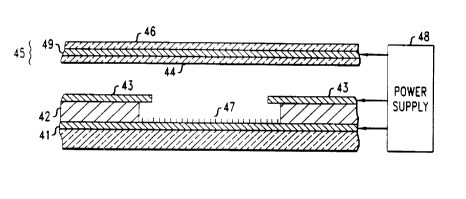
displays. Fig. 3 is a schematic cross section of a flat panel display using
thin film nanotube field emitters. The display comprises a cathode 41
including a plurality of nanotube emitters 47 and an anode 45 disposed
in spaced relation from the emitters within a vacuum seal. The anode
conductor 49 formed on a transparent insulating substrate 46 is provided
with a phosphor l;~yer 44 and mounted on support pillars (not shown).
Between the cathode and the anode and closely spaced from the emitters
is a perforated conductive gate layer 43. Conveniently, the gate 43 is
spaced from the c;~thode 41 by a thin insulating layer 42.
1o The space between the anode and the emitter is sealed and
evacuated, and vc,ltage is applied by power supply 48. The field-emitted
electrons from nanotube emitters 47 are accelerated by the gate
electrode 43 from multiple emitters 47 in each pixel and move toward
the anode conduci;ive layer 49 (typically a transparent conductor such as
indium-tin-oxide) coated on the anode substrate 46. A phosphor layer 44
is disposed between the electron emitters and the anode. As the
accelerated electrons hit the phosphor layer 44, a display image is
generated.
The nanotube emitter structures are also useful in microwave
2o vacuum devices such as a traveling wave tube (TWT). See, e.g., A.
Gilmour, Jr., Microwave Tubes, Artech House, 1986. Figs. 4A and 4B
schematically illustrate a TWT 50. The TWT contains an evacuated
tube 52, an electron source (here an electron gun 54), an input window
56 for introducing a microwave input signal, an interaction structure 58
where the electrons interact with the input signal, and a microwave
output window 60 where microwave power derived from the electrons is
taken out of the tube. Other components of the TWT are a focusing
magnet (not shown) to focus the beam of electrons through the
interaction structure 58, a collector 62 to collect the electron beam after
CA 02280234 1999-08-13
Bower-Zhou-Zhu 1-1-;3?
19
the output microwave power has been generated, and an internal
attenuator (not shown) to absorb microwave power reflected back into
the tube from mismatches in the output. The interaction region 58 is
typically a conductive helix for broadband applications and a coupled-
cavity region for high power applications.
The electron gun 54 generates, accelerates, and focuses an
electron beam to follow a desired trajectory. For TWT applications, a
long, thin electron beam at relatively low voltage and high current is
desirable. Electra~n guns range in configuration from, for example, a
1o planar cathode faced by a planar anode to more elaborate designs such
as Pierce guns, comical diode electrodes, concentric cylinders, and
spherical cap cathodes. (See, e.g., A. Gilmour, Jr., Microwave Tubes,
supra.) In operation of the TWT, an electron beam 64 is accelerated from
a cathode 66 by hiigh voltages applied to grids 68 and an anode 70, and
focused by control electrodes 72. The beam 64 is directed into the
interaction structure 58 where the beam 64 interacts with the
microwave input signal to be amplified as the electrons and the signal
travel together through the interaction structure 58. The electrons
advantageously travel at the same velocity as the microwave signal on
2o the interaction structure 58. The modulated electron beam generates an
amplified form of the input signal at the output 60.
The low field nanotube emitters of the invention are also useful as
cold cathodes in other field emission devices, including x-y matrix
addressable electron sources, electron sources for electron beam
lithography, and ;similar applications apparent to one skilled in the art.
The invention will be further clarified by the following examples,
which are intended to be exemplary.
CA 02280234 1999-08-13
Bower-Zhou-Zhu 1-1-37
Example 1
Single-walled carbon nanotubes were synthesized using a laser
ablation system such as shown in Fig. 1. A target of graphite mixed with
nickel/cobalt catalyst material was placed inside a furnace and heated to
5 1150°C under constant Ar flow. The target was ablated by the primary
beam of a pulsed hld:YAG laser (~, = 1064 nm) (a Quanta-Ray DCR-2A
laser). Materials :produced were in the form of a mat on a cold surface.
Transmission electron microscope, scanning electron microscope, and
Raman spectroscopy indicated that the raw material contained about 70
to vol.% single walled nanotubes having an average diameter of 1.4 to 1.5
nm, with the remaining 30 vol.% made up of amorphous carbon and
intermixed catalyst particles. The raw material was purified by
ultrasonically dispersing the nanotubes in a solvent and performing
multiple filtering.
~5 Three silicon wafers were pre-coated with a thin layer of iron,
chromium, and ahsminum, respectively, by sputtering or thermal
evaporation. The metallic layers were about 10 to 100 nm thick. (Iron is
a carbon-dissolving element, chromium a carbide-forming element, and
aluminum a low melting point metal. )
2o A air-spraying technique was used to dispose the nanotubes onto
the coated substrates. Specifically, a conventional atomizer spray nozzle
was attached to a high pressure gas line carrying argon at about 20 psi,
and a sprayer inlet was placed into a beaker filled with nanotubes
dispersed in methanol. A fine mist of solvent and nanotubes was
produced. The substrates were heated to about 200°C and located about
12 inches from them spray nozzle. This arrangement appeared to allow
the solvent to evaporate fully before the nanotubes contacted the
substrate surface. Smooth, as-sprayed films were produced.
CA 02280234 1999-08-13
Bower-Zhou-Zhu 1-1-.37
21
The coated substrates were placed under vacuum at 10~ tort and
heated at 800°C for three hours. This annealing process is believed to
promote chemical reactions between the nanotubes and iron, or the
nanotubes and chromium, or, in the case of aluminum, to allow molten
aluminum to coat portions of the nanotubes such that the nanotubes are
anchored upon cooling. After annealing, the films exhibited high
adhesion strength in the range of 1.2 to 1.7 kpsi as measured by the stud
pull test discussed herein. SEM examination further revealed that
application and removal of conventional Scotch~ brand-type tape did not
to pull the nanotubes off the substrate. And ultrasonication in methanol
similarly did not remove the nanotubes from the substrate.
Electron etxussion measurements were performed on these
adherent nanotube films in a vacuum chamber at 10~ tort and room
temperature. The experimental set-up is as described in W. Zhu et al.,
"Electron field emission from chemical vapor deposited diamond," J. Vac.
Sci. Technol., Vol. B14, 2011 (1996). Briefly, a voltage up to 2 kV was
applied to a spherical tungsten probe (0.5 mm in diameter) which
collects the current emitted from the grounded nanotube samples. A
precision step motor was used to vary the distance between the probe
2o and the sample surface with a step size of 3.3 ~.m. The current voltage
(I-V) characteristics were collected as a function of anode-cathode
distance, from about 6 ~m to about 320 ~,m.
Fig. 6A shows the electron emission current vs. applied voltage for
anode-cathode distances from 6.6 ~m to 320.1 ~,m, for the iron-coated
sample. It is clear' that smooth and consistent I-V curves are measured
in a history-independent, reproducible manner. Fig. 6B shows the same
data as Fig. 6A, but is plotted as log(I/V2) vs. 1/V, which shows the
characteristic Fowler-Nordheim linearity.
CA 02280234 2002-03-12
22
Fig. 7 shows that for the iron-coated sample, the turn-on field (i.e.,
the field that generates an emission current of 1 nA) is only 1.7 V/~,m,
and the threshold field (i.e., the field that generates an emission current
density of 10 mA/cm2) is 2.8 V/~,m. These values are an order of
magnitude less than fields required for other types of emitters, such as
molybdenum, silicon, and diamond emitters.
Similar emission properties were exhibited by the other nanotube
samples.
~o Ezample 2
Carbon nanotubes formed by a laser ablation process such as
described above were ground to fine powders and sonicated in solvent for
1 hour at room temperature. A thermoplastic polymer,
polyhydroxyaminoether (PHAE) from Dow Chemical Co., with a glass
is transition temperature less than room temperature was dissolved into
the nanotube/solvent suspension. After further sonification, the
suspension was transferred into a Teflo ~mold and air-dried in a fume
hood overnight. A black thin film formed in the Teflon mold was peeled
away. Films having nanotube weight percents of up to 50% were formed
2o in this manner, and cut into strips approximately 5 mm by 3 mm. The
films were mechanically stretched by applying a constant load at
temperatures of 90 to 100°C (above the polymer's glass transition
temperature), using varying loads. The films were typically stretched to
500% (final length over initial length) without fracture. After the
25 desired stretching ratio was reached, the sample was cooled down to
room temperature before releasing the load.
X-ray diffraction patterns were obtained for both stretched and
non-stretched samples, using a 1.5 kW Cu source, HOPG (002)
monochromator, and a two dimensional imaging plate detector (MAC
CA 02280234 1999-08-13
Bower-Zhou-Zhu 1-1-~37
23
Science DIP2000 with 2500x2500 pixels and 80 ~m pixel resolution) in
the transmission :mode. Structures of multi-walled nanotubes have been
previously studied. (See, e.g., O. Zhou et al., Science, Vol. 263, 1744
(1994). The diffraction pattern is dominated by a strong Bragg peak
centered around 3~.4~, which corresponds to the inter-shell spacing
within the same nanotube (referred to as the (002) peak).
When the nanotubes are randomly oriented, a powder di$'raction
ring with the d-space of 3.4A and uniform intensity distribution is
expected. If the nanotubes have a preferred orientation, the Bragg
to intensities will be concentrated at two spots at the intersections of the
plane defined by I~ (incident x-ray beam) and Q002 (reciprocal space
vector). A typical 2D x-ray diffraction pattern of an as-cast film is shown
in Fig. 8A. The data is plotted as 28 versus azimuth angle ~. The Bragg
peak corresponding to the nanotube inter-shell spacing, d002, was
centered around 26.1° in 2A (d=3.410, and is essentially a constant
with
respect to ~ from 0 to 360° (along the circumference of the diffraction
ring).
The x-ray diffraction pattern of a stretched (330%) film having
about 50 wt.% nanotubes is shown in Fig. 8B. The data was taken with
2o Ki perpendicular to the film surface and stretching direction. The (002)
Bragg intensity was concentrated at two spots centered at ~ = 90°
and
270°. The change in diffraction pattern from Fig. 8A shows that the
nanotubes in the .stretched film are aligned with their longitudinal axes
parallel to the strE~tching direction. By fitting and analyzing the 2D
intensity data, them fraction of nanotubes aligned, and the degree of
alignment are capable of being determined. In the sample of Fig. 8B,
58% of the nanotubes were substantially aligned along the stress
direction, with a cone of 20° mosaic angle.
CA 02280234 1999-08-13
Bower-Zhou-Zhu 1-1-37
24
The disper,;ion and alignment of the nanotubes were examined by
transmission electron microscopy (TEM). The composite samples were
cut into approximately 90 nm thick membranes using microtomy with a
diamond blade. ?'he nanotubes and impurity nanoparticles were
dispersed in the matrix without significant aggregation, and were
substantially wetted by the polymer, as reflected in Fig. 5, which shows
a film sample that was sliced parallel to the stretching direction
(indicated by the ;grows),
Other embodiments of the invention will be apparent to those
1o skilled in the art iiom consideration of the specification and practice of
the invention disclosed herein.