Note: Descriptions are shown in the official language in which they were submitted.
CA 02280593 1999-08-23
ID1035 K Farley - R E Epworth - D Watley
1
POLARISATION MODE DISPERSION COMPENSATION
Background of the Invention
When nominally circularly symmetric optical fibre is employed as a long
distance transmission path from an optical transmitter to an optical
receiver, the departures from perfect circular symmetry of that fibre can
be of a sufficient magnitude for the fibre to function as a concatenation of
birefringent elements of random relative orientation. Moreover that
orientation is liable to change with time.
When polarised light of any particular wavelength is transmitted through
a single element exhibiting uniform birefringence, that light is, in general,
resolved into two components (modes) propagating with two specific
different velocities, and so possessing different transit times of
propagation through that element. For each of two particular orthogonal
states of polarisation (SOPs), known as the principal SOPs, the light is
not resolved into different components, but propagates at a single
velocity with a single transit tirne, i.e. propagates as a single
(polarisation) mode. These principal SOl~'s are aligned with the principal
axes of birefringence of the element. For light launched into the element
with either one of these two principal SOPs, the SOP of the light remains
unchanged in its passage through the element. For light launched into
the element with any other SOP, that light is resolved in its passage
through the element into two orthogonal components aligned with the
principal axes of the element and propagating with different velocities.
As the result in the velocity difference, the relative phase of the two
components at the far end of the element is generally not the same as
that at the launch (input) end, and so the light emerging at the far end
generally emerges with an SOP that is different from that with which it
entered the element. This characteristic can be conceptualised as the
SOP of the light evolving in a cyclic manner in its passage through the
element.
CA 02280593 1999-08-23
-2-
When polarised light is transmitted through a concatenation of elements,
each exhibiting uniform birefringence, but whose principal axes are not
all co-aligned, then, even if that light is not resolved into two components
by the first element of the concatenation, it will be so resolved by a later
element. Then each of those two elements will itself be resolved into two
further components by an element further along the concatenation, and
so on. It can be demonstrated that for any such concatenation there
exists a specific pair of orthogonal SOPs having the property that light
launched with either SOP into the concatenation propagates through it
with a single transit time. The transit is faster for one of the SOPs than
for the other, and the difference in transit time, the differential group
delay (DGD), is a measure of the first order polarisation mode dispersion
(PMD) of the concatenation. (The term first order PMD is employed in
this specification to denote the DGD in respect of a particular
wavelength, thereby excluding from its ambit consideration of second
order PMD effects which describe the wavelength dependence of that
DGD.) For neither one of this specific pair of orthogonal SOPs is the
launch SOP maintained in the passage of the light through the
concatenation, and the light emerges at the far end with an SOP that is
in general different from that with which it was launched. The emergent
SOP for one of the single transit time launch SOPs is orthogonal to the
emergent SOP for the other single transit time launch SOP. For any
launch SOP that is not one of the single transit time launch SOPs, the
emergent light is composed of two components (polarisation modes),
generally of unequal amplitude, which have propagated through the
concatenation with different transit times, respectively the previously
mentioned fast and slow single transit times of the concatenation.
By analogy with the single uniform birefringence element situation, the
two single transit time launch SOPs for the concatenation are often
referred to as the principal SOPs of the concatenation. Having regard to
CA 02280593 1999-08-23
-3-
the fact that for such a concatenation the single transit time input
(launch) SOPs are, in general, different from the corresponding output
(emergence) SOPs, reference in this specification will be made to input
principal SOPs (IPSPs) and to output principal SOPs (OPSPs). From
consideration of principles of reciprocity, it will be evident that the IPSPs
for one direction of propagation through the concatenation are the
OPSPs for the other, and vice versa.
The presence of first order polarisation mode dispersion (PMD) in a
1 o transmission path - the difference between the fast and slow single
transit times (DGD) - is liable to be a problem when its magnitude
becomes significant compared with the bit period of traffic propagating in
the transmission path. Under these circumstances there will be
significant pulse broadening at the receiver when bits are launched into
the transmission path with an SOP that the transmission path divides into
fast and slow single transit time components (modes) of equal power. In
principle, this pulse broadening effect could be avoided by taking steps
to ensure that the bits are always launched into the transmission path
with SOPs matched with one of the IPSPs of the transmission path so
that they always propagate, either exclusively with the fast transit time, or
exclusively with the slow one, i.e. so that they always propagate in a
single mode. However there are difficulties with achieving this in
practice. The primary reason for this is that the IPSPs vary with time,
and so an active SOP alignment system would be required. Additionally,
identification of the IPSPs typically requires access to both ends of the
transmission path, and so the active SOP alignment system situated at
the transmitter end of the transmission path would require a feedback
control signal from the receiver end of that transmission path.
An alternative approach to the avoidance of the problems presented by
first order PMD is a compensation approach that involves allowing the
bits to be launched into the transmission path with an SOP that the
CA 02280593 1999-08-23
-4-
transmission path divides into two components (modes) propagating with
different (fast and slow) transit times, and providing an active system at
the receiver end which separates the two components, subjects the
separated components to controlled variable differential delay to restore
synchronisation of the components, and then recombines them.
An example of the PMD compensation approach is described in United
States Patent No 5 659 412. At the receiver, the signal received from
the transmitter via the transmission path is fed to a polarisation beam
splitter via a polarisation state controller The outputs of the polarisation
beam splitter are fed to separate detectors provided with associated
clock extraction circuits, and the phase relationship between the two
extracted clock signals is determined. The resulting phase difference
signal is used to control the polarisation state controller in such a way as
to maximise the phase difference. This phase difference is at a
maximum when the polarisation state controller is operative to map the
OPSPs of the transmission path on to the principal polarisation states of
the polarisation beam splitter, and under these conditions the
polarisation beam splitter is operative to separate the component of the
signal launched into the transmission path that propagates through it
with the 'fast' transit time from the component that propagates through it
with the 'slow' transit time. In one of the embodiments specifically
described, the electrical output of the detector providing the phase-
leading clock signal is delayed by the amount corresponding to the
measured phase difference between the two extracted clock signals, the
DGD, and then the two electrical signals are combined. In the other
embodiment specifically described, the two detectors receive only a
tapped fraction of the total optical power outputs from the polarisation
beam splitter, while the remainder of that power, after the imposition of
3 o an optical delay upon the leading component, is optically combined and
detected using a third detector. Thus it is seen that the approach of USP
5 659 412 necessarily requires the use of at least two detectors capable
CA 02280593 1999-08-23
-5-
of operating at the bit rate, some embodiments requiring three such
detectors. Moreover operation of the device is complicated by the need
to allow for the occurrence of occasions in which either one of the IPSPs
of transmission path approaches and passes through coincidence with
the SOP of the signal being launched into that transmission path. Under
these conditions there is a large disparity in power level between the two
outputs of the polarisation beam splitter.
Another option similarly involves allowing the bits to be launched into the
transmission path with an SOP that the transmission path divides into
two components (modes) propagating with different (fast and slow)
transit times, and providing an active polarisation controller at the
receiver end. However in this instance the output of the polarisation
controller is fed to a birefringent element of fixed, rather than variable
DGD. Under these circumstances the adverse effects of first order PMD
are not eliminated, but are merely alleviated. This is because whenever
the DGD of the transmission path differs from that of the birefringence
element, that birefringence element can provide only partial
compensation, rather than complete compensation.
An example of this type of partial compensation option is described in the
specification of United States Patent No. 5 473 457. This specification
describes using a length of polarisation maintaining fibre as the fixed
DGD birefringent element, and the data is impressed as amplitude
modulation of an optical carrier which is itself frequency modulated in
order to provide a control signal at the receiver which can be used for
regulating the polarisation controller. This frequency modulation is a
significant drawback not least because it adds to the bandwidth of the
data.
Another example of this type of partial compensation option is described
by T Takahashi et al in an article entitled `Automatic compensation
CA 02280593 2008-05-23
77550-45
-6-
technique for timewise fluctuating polarisation mode dispersion in in-line
amplifier systems', Electronics Letters, Vol. 30, No 4 pp 348-9, 17
February 1994. These authors similarly employ a length of polarisation
maintaining fibre as their fixed DGD birefringent element, but generate
their control signal for regulating the operation of the polarisation
controller by deriving a measure of the magnitude of the frequency
component of the detected signal at the receiver that corresponds to half
the bit-rate, specifically the frequency component at 5GHz for a 10Gbit/s
data rate. A disadvantage of this approach to generating the control
1o signal required for regulating the polarisation controller is the limited
response speed that can be obtained for this form of control signal
generation. In this context it may be noted that, while the DGD of
overhead and land cables rriay be expected to move with periods of the
order of minutes or hours, the IPSPs can be expected to move with
periods of the order of seconds, while, in the case of exposed fibres that
are subject to being accidentally knocked, the corresponding period is
liabl.e-to be sub-second.
Summary of the Invention
According to one aspect of the present invention,
there is provided a method of transmitting a clocked digital
optically polarised signal from a transmitter to a receiver
via a transmission path liable to exhibit polarisation mode
dispersion (PMD), the method comprising: launching the
signal into the transmission path with its state of
polarisation (SOP) modulated in a-manner which, when
represented on a Poincare sphere, has an oscillatory
rotational component at a frequency fl about a first axis of
the sphere and an oscillatory rotational component at a
frequency f2 about a second axis of the sphere that is
orthogonal to said first axis, and where fl# f2, fl# 2f2,
and f2 ~ 2f1i and at the other end of said transmission path:
CA 02280593 2008-05-23
77550-45
6a
feeding the clocked digital optical signal emergent
therefrom through an adjustable birefringence element;
detecting output of the adjustable birefringence element
with a photodetector; extracting a clock signal having
frequency components at fl and f2 from output of the
photodetector using a clock extraction circuit; and
regulating the birefringence of the adjustable birefringence
element with a feedback control loop so as to minimise the
amplitude of said frequency components, wherein said
frequency components are employed as control signals in said
feedback control loop.
According to another aspect of the present
invention, there is provided a method of transmitting a
clocked digital optically polarised signal from a
transmitter to a receiver via a transmission path liable to
exhibit polarisation mode dispersion (PMD), the method
comprising: launching the signal into the transmission path
with its state of polarisation (SOP) modulated in a manner
which, when represented on a Poincare sphere, has an
oscillatory rotational component at a frequency fl about a
first axis of the sphere and an oscillatory rotational
component at a frequency f2 about a second axis of the sphere
that is orthogonal to said first axis, and where fl # f 2, f 1 #
2f2, and f2 # 2f1; at the other end of said transmission path:
feeding the clocked digital optical signal emergent
therefrom through an adjustable birefringence element;
detecting output of the adjustable birefringence element
with a photodetector; extracting a clock signal having
frequency components at fl, 2f1, f2r and 2f2 from output of
the photodetector using a clock extraction circuit; and
regulating the adjustment of the adjustable birefringence
element with a feedback control loop so as to substantially
match the magnitude of its first order PMD with that of the
CA 02280593 2008-05-23
77550-45
6b
transmission path, and to bring the fast axis input
principal state of polarisation (IPSP) of the birefringent
element into substantial alignment with the slow axis output
principal states of polarisation (OPSP) of the transmission
path, wherein said frequency components are employed as
control signals in said feedback control loop.
According to still another aspect of the present
invention, there is provided a method of transmitting a
clocked optically polarised signal from a transmitter to a
receiver via a transmission path liable to exhibit
polarisation mode dispersion (PMD), the method comprising:
launching the signal into the transmission path with its
otate of polarisation (SOP) modulatcd in a manner which,
when represented on a Poincare sphere; has an oscillatory
rotational component at a frequency fl about a first axis of
the sphere and an oscillatory rotational component at a
frequency f2 about a second axis of the sphere that is
orthogonal to said first axis, and where fl # f2, fl# 2f2,
and fz # 2f1.
According to yet another aspect of the present
invention, there is provided a method of transmitting a
clocked optically polarised signal comprising: launching the
signal into a transmission path with its state of
polarisation (SOP) modulated in a manner which, when
represented on a Poincare sphere, has an oscillatory
rotational component at a frequency fl about a first axis of
the sphere and an oscillatory rotational component at a
frequency f2 about a second axis of the sphere that is
orthogonal to said first axis, and where fl # f2, fl# 2f2,
and f2 # 2f1.
According to a further aspect of the present
invention, there is provided a method of receiving a clocked
CA 02280593 2008-05-23
77550-45
Gc
optical signal transmitted via a transmission path liable to
exhibit polarisation mode dispersion (PMD), the method
comprising: feeding the clocked optical signal through an
adjustable birefringence element; detecting output of the
adjustable birefringence element with a photodetector;
extracting a clock signal having frequency components at f,
and f2 with a clock extraction circuit; and regulating the
birefringence of the birefringent element with a feedback
control loop so as to minimise the amplitude of said
frequency components, wherein said frequency components are
employed as control signals in said feedback control loop,
and the clocked optical signal having been launched into the
transmission path with its state of polarisation (SOP)
modulated in a manner which, when represented on a Poincare
sphere, has an oscillatory rotational component at a
frequency f1 about a first axis of the sphere and an
oscillatory rotational component at a frequency f2 about a
second axis of the sphere that is orthogonal to said first
axis, and where fl # f2, fl # 2f2, and f2 # 2f1.
According to yet a further aspect of the present
invention, there is provided an optical transmission system
comprising a transmitter, a receiver, and a transmission
path liable to exhibit polarisation mode dispersion (PMD)
arranged to transmit a clocked optically polarised signal
from the transmitter to the receiver via the transmission
path wherein the signal is launched into the transmission
path with its state of polarisation (SOP) modulated in a
manner which, when represented on a Poincare sphere, has an
oscillatory rotational component at a frequency fl about a
first axis of the sphere and an oscillatory rotational
component at a frequency f2 about a second axis of the sphere
that is orthogonal to said first axis, and where fl# fZ, fl#
2f2, and f2 # 2f1r wherein at the other end of said
CA 02280593 2008-05-23
77550-45
6d
transmission path the clocked optical signal emergent
therefrom is fed through an adjustable birefringence element
before being detected by a photodetector and fed to a clock
extraction circuit to provide a clock signal having
frequency components at fl and f2, which frequency components
are employed as control signals in a feedback control loop
regulating the birefringence of the birefringent element so
as to minimise the amplitude of said frequency components.
According to still a further aspect of the present
invention, there is provided a transmitter arranged to
provide a clocked optically polarised signal wherein the
signal is launched into a transmission path with its state
of polarisation (SOP) modulated in a manner which, when
represented on a Poincare sphere, has an oscillatory
rotational component at a frequency fl about a first axis of
the sphere and an oscillatory rotational component at a
frequency f2 about a second axis of the sphere that is
orthogonal to said first axis, and where f 1 # f2, f 1 # 2f 2,
and f2 # 2f1.
According to another aspect of the present
invention, there is provided a receiver for receiving a
clocked optical signal transmitted via a transmission path
liable to exhibit polarisation mode dispersion (PMD), the
signal having been launched into the transmission path with
its state of polarisation (SOP) modulated in a manner which,
when represented on a Poincare sphere, has an oscillatory
rotational component at a frequency fl about a first axis of
the sphere and an oscillatory rotational component at a
frequency f2 about a second axis of the sphere that is
orthogonal to said first axis, and where fl# f2, fl# 2f2,
and f2# 2f1, the receiver comprising: an adjustable
birefringence element; a photodetector; a control extraction
CA 02280593 2008-05-23
77550-45
6e
circuit; and a feedback control loop, wherein the clocked
optical signal emergent from the transmission path is fed
through the adjustable birefringence element before being
detected by the photodetector and fed to the clock
extraction circuit to provide a clock signal having
frequency components at fl and f2, wherein said frequency
components are employed as control signals in a feedback
control loop regulating the birefringence of the
birefringent element so as to minimise the amplitude of said
frequency components.
According to yet another aspect of the present
invention, there is provided a method of performing
polarisation mode dispersion (PMD) compensation on a
received optically polarised signal having had its state of
polarisation (SOP) modulated in a manner which, when
represented on a Poincare sphere, has an oscillatory
rotational component at a frequency fl about a first axis of
the sphere and an oscillatory rotational component at a
frequency f2 about a second axis of the sphere that is
orthogonal to said first axis, and where f1 $ f 2, f1 # 2f2i
and f2 # 2f1i the method comprising: at a receiver: feeding
the signal through a series combination of a polarisation
state controller and a variable birefringence birefringent
element; detecting output of the series combination of the
polarisation state controller and the variable birefringence
birefringent element with a photodetector, wherein said
variable birefringence birefringent element comprises a
length of polarisation maintaining fiber provided at an
intermediate point in its length with a controllable
variable strength polarisation mode coupler.
According to another aspect of the present
invention, there is provided an optical receiver comprising
CA 02280593 2008-05-23
77550-45
6f
a polarisation state controller, a variable birefringence
birefringent element, a photodetector, and arranged to be
coupled to a transmission path, wherein a signal emergent
from the transmission path, having been launched into the
transmission path with its state of polarisation (SOP)
modulated in a manner which, when represented on a Poincare
sphere, has an oscillatory rotational component at a
frequency fl about a first axis of the sphere and an
oscillatory rotational component at a frequency f2 about a
second axis of the sphere that is orthogonal to said first
axis, and where fl # f2, fl # 2f2, and f2 # 2f1, is fed through
the series combination of the polarisation state controller
and variable birefringence birefringent element before being
detected by the photodetector, wherein the variable
birefringence birefringent element comprises a length of
polarisation maintaining fiber provided at an intermediate
point in its length with a controllable variable strength
polarisation mode coupler.
According to yet another aspect of the present
invention, there is provided a method of transmitting an
optically polarised signal from a transmitter to a receiver
via a transmission path liable to exhibit polarisation mode
dispersion (PMD), the method comprising: launching the
signal into a transmission path with its state of
polarisation (SOP) modulated in a manner which, when
represented on a Poincare sphere, has an oscillatory
rotational component at a frequency f,_ about a first axis of
the sphere and an oscillatory rotational component at a
frequency f2 about a second axis of the sphere that is
orthogonal to said first axis, and where f 1 # f2, f 1 # 2f 2,
and f2 # 2f1; and at the receiver: feeding the signal
emergent from the transmission path through a series
combination of a polarisation state controller and a
CA 02280593 2008-05-23
77550-45
6g
variable birefringence birefringent element; detecting
output of the series combination of the polarisation state
controller and the variable birefringence birefringent
element with a photodetector, wherein said variable
birefringence birefringent element comprises a length of
polarisation maintaining fibre provided at an intermediate
point in its length with a controllable variable strength
polarisation mode coupler.
Some embodiments of the invention may provide a
method of PMD compensation using a polarisation controller
in association with a variable DGD compensation element, but
without having to have recourse to the use of more than one
detector for generating a control signal for regulating the
polarisation controller and the DGD compensation unit.
Some embodiments of the invention may provide a
method of PMD compensation using a polarisation controller
in association with a fixed DGD compensation element, the
method affording the capability of relatively fast control
response times.
Some embodiments modulate the polarisation state
of light launched into the transmission path. This
CA 02280593 1999-08-23
-7-
modulation is of a form that, when represented on a Poincare sphere,
has an oscillatory rotational component at a frequency f, about a first axis
of the sphere, and an oscillatory rotational component at a frequency f2
about a second axis of the sphere that is orthogonal to the first axis, and
where f, # f2, f, # 2f 2, and f2 # 2f,.
Other features and advantages of the invention will be readily apparent
from the following description of preferred embodiments of the invention
from the drawings and from the claims.
Brief Description of the Drawings
Figure 1 is a schematic diagram of an optical transmission system,
Figures 2 and 3 are schematic diagrams respectively of the transmitter and
receiver of the optical transmission system of Figure 1,
Figures 4, 5 and 6 are Poincare diagrams illustrating the SOP modulation
applied by the SOP modulator of the transmitter of Figure 2,
Figures 7 depicts a set of timing diagrams illustrating how the alteration of
the division of power between the fast and slow transit time
components of pulses suffering PMD affects the timing of their
centres of gravity,
Figure 8 is a plot of worst case receiver sensitivity penalty plotted as a
function of polarisation path PMD both in respect of an
uncompensated transmission system and in respect of a PMD
compensated system using fixed amplitude PMD compensation.
Figure 9 is a schematic diagram of an alternative form of receiver of the
transmission system of Figure 2, and
Figures 10 and 11 are schematic diagrams of alternative forms of
controllable variable birefringence PMD compensation element
employed in the receiver of Figure 9.
Detailed Description of Preferred Embodiments
Referring to Figure 1, and optical receiver 10 is optically coupled with an
optical transmitter 11 via an optical fibre transmission path 12 that
exhibits polarisation mode dispersion (PMD) and that may include along
its length one or more optical amplifiers 13, for instance optically pumped
CA 02280593 1999-08-23
-8-
erbium doped fibre amplifiers. The major components of the optical
transmitter 11 are schematically depicted in Figure 2, and comprise an
optical source 20 emitting polarised light, such as a semiconductor laser
diode; a polarisation state modulator 21; and a data modulator 22 that
digitally modulates the optical output of the optical source 20 with
clocked data applied by way of terminal 23. (In Figure 2, the polarisation
state modulator 21 is specifically illustrated as preceding the data
modulator 22, but it may be preferred, or indeed necessary, to reverse
this order. For instance, the reverse order is necessary if the data
modulator is of a form that requires a specific SOP, such is generally the
case in respect of lithium niobate modulators.) The polarisation
modulator is driven by two oscillators 24 and 25 respectively operating at
frequencies f, and f2, where f, # f2, f, # 2fZ, and f2 # 2f,. The output of
oscillators 24 and 25 are employed by the SOP modulator 21 to
modulate the SOP of the light directed into the modulator in a manner
which, when represented on a Poincare sphere, have oscillatory
rotational components respectively at the frequencies f, and f2
respectively about first and second orthogonal axes of the sphere.
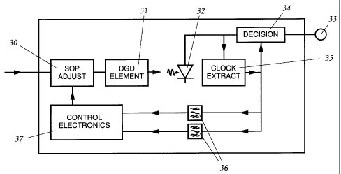
Correspondingly, the major components of the optical receiver 10 are
schematically depicted in Figure 3, and comprise an SOP controller 30, a
DGD compensation element 31 a photodetector 32 whose electrical
output is fed to an output terminal 33 of the receiver via decision circuitry
34, and also to a clock extraction circuit 35. The output of the clock
extraction circuit provides a clock input signal to regulate the operation of
the decision circuitry 34, and is also fed to two filters 36 respectively
tuned to the frequencies f, and f2. The outputs of these two filters are fed
as control signals to control electronics 37 that regulates the operation of
the SOP controller 30.
CA 02280593 1999-08-23
-9-
The way in which the SOP modulation at frequencies f, and f2 provided
by the SOP modulator 21 of the transmitter 20 gives rise to amplitude
modulation, at frequencies f,, f2, 2f,, and 2f2, of the clock signal extracted
at the receiver 10 by clock extraction circuitry 35 is conveniently
explained by reference to the Poincare sphere diagrams of Figures 4, 5
and 6. A Poincare sphere is a way of representing all possible states of
polarisation of light (linearly, circularly and elliptically polarised states)
as
points on the surface of a sphere. In the case of the Poincare sphere 40
of Figure 4 the poles L and R represent circularly polarised states. On
the great circle `equator' through HQV and P are represented all the
linearly polarised states, and between the poles and the equator lie all
the elliptically polarised states. It may be noted that any pair of
orthogonally polarised states lie at diametrically opposed points on the
Poincare sphere. When polarised light is transmitted through a medium
exhibiting uniform birefringence, the SOP with which the light is launched
into the medium is generally different from that with which the light
emerges from that medium. However there is a particular pair of
orthogonal SOPs for which launch and emergence SOPs are identical.
These two orthogonal SOPs are termed eigenstate SOPs, and define the
2 o eigenaxis of that medium. The change in SOP produced by passage of
polarised light through the medium is represented by a rotation on the
Poincare sphere about the eigenaxis through an angle determined by the
strength of the birefringence. In the case of materials exhibiting linear
birefringence, such as a uniaxial crystal of calcite, the eigenstates are
linearly polarised SOPs, and so the eigenaxis lies in the equatorial plane
of the Poincare sphere of Figure 4. Linear birefringence is also exhibited
by optical fibre that does not possess perfect circular symmetry, for
instance as the result of providing the fibre core with a structure
producing a non-circularly symmetric lateral component of strain. In this
instance the strength of the linear birefringence exhibited by the fibre is
adjustable by the application of an adjustable amount of additional lateral
strain, for instance by squeezing the fibre. If therefore the light from the
CA 02280593 1999-08-23
-10-
source 20 enters the SOP modulator 21 in the form of linearly polarised
light, the SOP modulator may be composed of two frequency modulated
squeezer elements, for instance piezoelectrical squeezer elements
operating in tandem upon the fibre. In respect of one preferred
embodiment, if the SOP of the light entering the SOP modulator 21 is
represented by the point H on the Poincare sphere 40 of Figure 4, then
the orientation of the first piezoelectric squeezer element of the SOP
modulator 21 is oriented so that its eigenaxis lies along the line PQ. The
mean retardation provided by this first squeezer element is chosen to be
V4, and so is represented on the Poincare sphere as 7r/2 rotation in the
clockwise sense as seen from the P end of the eigenaxis.
Superimposed upon this n/2 rotation is an oscillatory modulation at the
frequency f, of an amplitude. that corresponds to the sweeping out of an
arc 41 on the Poincare sphere 40 that lies on the great circle through
HLV and P, is centred on L, and subtends an angle 20 at the centre of
the sphere. The second piezoelectric squeezer element of the SOP
modulator 21 is then oriented so that its direction of squeeze is aligned
at 7r,/4 with respect to that of the first squeezer element. The eigenaxis of
the second squeezer element is therefore at 7r/2 on the Poincare sphere
with respect to that of the first squeezer element, i.e. the eigenaxis of the
second squeezer element is along the direction HV. The mean rotation
provided by this second squeezer element is also chosen to be X/4 and
is represented on the Poincare sphere as an/2 rotation in the clockwise
sense as seen from the H end of its eigenaxis. The arc 41 is therefore
mapped on to the position of arc 42 which lies on the equatorial great
circle through HQV and P, is centred on P, and similarly subtends an
angle 20 at the centre of the sphere. Superimposed on this 7/2 rotation
is an oscillatory modulation at the frequency f2 of an amplitude that, in
the absence of the f, modulation of the first squeezer element,
corresponds to the sweeping out of an arc 43 which lies on the great
circle through QLP and R is centred on P and subtends an angle 2~ at
the centre of the sphere.
CA 02280593 1999-08-23
-11-
It is not necessary for both retarders of the SOP modulator to be variable
strength linear birefringence retarders. Either or both may alternatively
be variable strength circular birefringence retarders. Such a device may
for instance be constituted by a Faraday rotator. An alternative form of
variable strength circular birefringence retarder, one which does not
employ bulk optics, but in which the light propagates from end to end in
an optical fibre, is the type of device described in United States Patent
No 5 115 480 with particular reference to its Figures 1, 2 and 3.
The manner of operation of an alternative embodiment of SOP modulator
21, one that employs a pair of variable strength circular birefringence
retarders, will now be explained with reference to the Poincare sphere of
Figure 5. As before, the light entering the SOP modulator is plane
polarised in a direction represented by the point H. The first variable
strength circular birefringence retarder of the SOP modulator is driven
with an oscillatory signal of frequency f2 with an amplitude that
corresponds to the sweeping out of an arc 51 on the Poincare sphere 50
that lies on the equatorial great circle through HQV and P, is centred on
H, and subtends an angle 2~ at the centre of the sphere. Between this
first variable strength circular birefringence retarder and the second are
located two quarter-wave (fixed strength) linear birefringence retarders.
The first of these quarter-wave retarders is oriented at 45 to the first so
that, on the Poincare sphere, its eigenaxis is aligned in the direction PQ,
and so this quarter-wave retarder has the effect of mapping the arc 51
on to the arc 52 that lies on the great circular through HLV and R, is
centred on L, and similarly subtends an angle 2~ at the centre of the
sphere. The second of the quarter-wave linear birefringence retarders is
oriented so that, on the Poincare sphere, its eigenaxis is aligned in the
direction HV. Accordingly this second quarter-wave retarder has the
effect of mapping the arc 52 on to the arc 43, that lies on the great circle
QLP and R, is centred on P, and also subtends an angle 2~ at the centre
CA 02280593 1999-08-23
-12-
of the sphere. The second variable strength circular birefringence
retarder is driven with an oscillatory signal of frequency f, with an
amplitude that, in the absence of the f2 modulation of the first variable
strength circular birefringence retarder, corresponds to the sweeping out
of the arc 42 which lies on the equatorial great circle through HQV and P,
is centred on P, and subtends an angle 20 at the centre of the sphere.
Referring now to the Poincare sphere 60 of Figure 6, it is assumed, for
simplicity of analysis, that the output from the SOP modulator is applied
directly to the input of the PMD transmission path 12 without any
intervening change of SOP. Accordingly the input SOP to the
transmission path has a mean state corresponding to the linearly
polarised state P. The transmission path has fast and slow IPSPs
(launch principal SOPs) that in the course of time are liable to wander all
over the surface of their sphere while at all time remaining diametrically
opposed to each other. At some instant these fast and slow IPSPs may
be represented in the Poincare sphere respectively at locations F and S.
Ignoring in the first instance the polarisation state modulations at
frequencies f, and f2, light is being launched into the PMD transmission
path 12 with an SOP given by point P, and at this instant neither of the
IPSPs is coincident with P. Therefore some of the light propagates
through the transmission path 12 with the fast transit time, while the
remainder propagates through with the slow transit time. The amplitudes
of the fast and slow components is determined by the angle POS = 2y
between the PQ and FS axes. The amplitude of the fast component
varies with sin 2y, while that of the slow component varies with cos 2yr.
The effect of the SOP modulations at frequencies f, and f2 is to produce a
modulation of the division of optical power between the component
propagating through the PMD transmission path with the fast transit time
and the component propagating through it with the slow transit time. The
CA 02280593 1999-08-23
-13-
manner in which the arises may easily be seen by considering certain
specific orientations of the FS axis defined by the IPSPs. If this FS axis
is aligned with the HV axis, then 2yr = 7r/2, with the result that the launch
power is divided equally between the component propagating through
the PMD transmission path 12 with the fast transit time, and the
component propagating with the slow transit time. The SOP modulation
at frequency f2 described by arc 43 does not involve any modulation of
the angle 2yr, and therefore the division of power between the fast and
slow transit time components is unaffected by this SOP modulation at
frequency f2. This SOP modulation at frequency f2 described by arc 43
will similarly involve no modulation of the angle 2y for any orientation of
the FS axis lying in the equatorial plane containing HQV and P. On the
other hand, the SOP modulation at frequency f, described by arc 42 will
produce a corresponding modulation (by 0) of the angle 2yr, and so will
produce a corresponding modulation of the division of power between
the fast and slow transit time components propagating through the PMD
transmission path 12. When 2y =ic/2 (i.e. when the FS and HV axes are
aligned) the division of power modulation is, for small values of 0, related
approximately linearly to the SOP modulation frequency f,, and so the
2 o ratio of the division of power modulation at 2f, to that at f, is small.
This
ratio increases to a maximum as the orientation of the FS is swept round
in the equatorial plane into alignment with the PQ axis (i.e. as 2yr is
reduced from 2yr = ir/2 to 2W = 0).
Attention is now returned to the situation in which the FS axis is aligned
with the HV axis and a pulse of light of pulse width co is launched into the
PMD transmission path 12 from the transmitter 11. The angle 2W = M/2,
and so when the pulse emerges from the far end of the PMD
transmission path 12, it is found to be composed of two equal amplitude
components which have propagated through the transmission path 12
with different transit times. The SOP modulation at f, described by arc
42 modulates the angle yr over the range Tc/2 0. The timing diagrams
CA 02280593 1999-08-23
-14-
(a) and (b) of Figure 7 depict the response of the photodetector 30
respectively to the arrival at the receiver 10 of the fast transit time
component and to that of the slow transit time component for the launch
SOP condition corresponding to the end of the arc 42 that is nearer V,
i.e. when 2y, = 7r/2 + 0. The response to the fast transit time component
is ahead of that to the slow transit time component by the differential
group delay time tDGD, which is the polarisation mode dispersion of the
transmission path 12. Because in this instance 2yr >n/2, the relative
amplitude of the response of the photodetector 30 to the fast transit time
component (0.5-m) is smaller than that of its response to the slow transit
time component (0.5+m). The resultant of these two responses is shown
in timing diagram (c) of Figure 7, and it can readily be shown that the
centre of gravity, CofG1, of this resultant response is delayed m x tDGD
with respect to the centre of gravity (not shown) pertaining, when 2y,
7r/2.
The timing diagrams (d) and (e) of Figure 7 depict the response of the
photodetector 30 respectively to the arrival of the fast and slow transit
time components for the launch SOP condition corresponding to the
other end of the arc 42, the end nearer H, i.e. when 2yr = 7r/2 - 0. The
resultant of these two responses is shown in timing diagram (f) of Figure
7, and it can readily be shown that the centre of gravity, CofG21 of this
resultant response is advanced m x tDGD with respect to the centre of
gravity pertaining where 2yr= 7r/2.
The clock extraction circuit 35 produces clock pulses that have a centre
of gravity centred on the average timing of a preceding train of pulses,
and so it is seen that, provided that frequency f, is long compared with
the duration of the pulse train averaged by the clock extraction circuit,
the clock output will have a modulation component at frequency f, whose
amplitude is directly related to the magnitude of the PMD exhibited by
transmission path 12.
CA 02280593 1999-08-23
-15-
From the foregoing, it is evident that, if the SOP modulation amplitude 0
is known, it is in principle possible to determine the magnitude of the
PMD exhibited by transmission path to be determined from a measure of
the magnitude of the f, component of the extracted clock signal
whenever the IPSPs are known to be aligned with the HV axis. On its
own, this lacks practical utility in the absence of knowledge as to when
the IPSPs are so aligned with the HV axis, but the situation can be
somewhat generalised by additionally taking into account the amplitudes
of the components of the clock output at frequencies f2 and 2f2. By
including knowledge of the magnitudes of these two additional variables
it is possible to determine the magnitude of the PMD for any orientation
of the IPSP axis.
The foregoing analysis was predicated on the SOP of the light being
launched into the SOP modulator 21 being known and, without loss of
generality, the analysis developed by way of specific example for the
case in which this known SOP is a linearly polarised state arbitrarily
represented by the point P on the Poincare sphere. If however for some
reason the SOP with which light is launched into the SOP modulator 21
is not known, or is liable to vary with time, then it could be possible for
this launch SOP to become aligned with the eigenaxis of one of the two
variable strength birefringence elements of the SOP modulator 21.
Under these conditions the modulation of the birefringence strength of
that particular element would produce no corresponding modulation of
the output SOP of the SOP modulator. The problem that this possibility
presents can however be circumvented by providing the SOP modulator
21 with a third variable strength birefringence element modulated at a
frequency f3, where f, # f3 # f2, 2f, # f3 # 2f2 and f, #2f3 #f2, and arranged
so that its eigenaxis is orthogonal with respect to the eigenaxes of the
other two variable strength birefringence elements of SOP modulator 21.
CA 02280593 1999-08-23
-16-
The foregoing analysis has not taken account of the birefringence of the
SOP controller 30 and that of the DGD compensation element 31. A
rigorous analysis treats them as incorporated as part of an extended
transmission path, a path that extends all the way from the transmitter 11
to the detector 32 of the receiver 10. An alternative way of considering
the effect of the controller 30 and compensation element 31 is to treat
the controller as an element that can map the OPSPs of the transmission
path 12 on to the IPSPs of the compensation element 31. If the DGD of
the compensation element matches that of the transmission path 12, and
if the controller 30 is able to map the fast transit time OPSP of the
transmission path 12 on to the slow transit time IPSP of the
compensation element, then the extended transition path between the
transmitter 11 and the detector 32 of the receiver 10 (i.e. the series
combination of the transmission path 12, the SOP controller 30 and the
compensation element 31) has a zero DGD. Thus the effect of the SOP
controller and the compensation element has, in these circumstances,
been such as to compensate fully for the first order PMD of the
transmission path 12.
Perfect compensation of this sort may be more than is truly necessary in
a practical situation if a less perfect alternative can be implemented in a
less expensive way, and yet still provide acceptable performance. A
convenient way of assessing performance is in terms of receiver
sensitivity penalty. Trace 80 of Figure 8 depicts a typical receiver
sensitivity penalty (increase in receiver received signal power required to
meet a given bit error rate) characteristic plotted as a function of DGD
expressed as a percentage of bit period, this characteristic being in
respect of a notional uncompensated transmission path under worst
case conditions (i.e. under the condition that the signal launched into this
notional transmission path is launched with an SOP that this notional
transmission path divides into fast and slow transit times components of
equal amplitude.
CA 02280593 1999-08-23
-17-
From this trace it is seen that there is a 1 dB penalty in receiver
sensitivity
when the DGD has reached about 30% of the bit period, i.e. for a
lOGbit/s system the power requirement at the receiver to achieve a
specific BER (e.g. 10'9) in the absence of any DGD has to be increased
by 1dB.
Consider now the situation in which the transmission path 12 is followed
by the SOP controller 30 and DGD compensation element 31 having a
specific fixed value of DGD, for instance 80%, constituted for instance by
a specific length of polarisation maintaining fibre. For the extended
transmission path comprising the series combination of the transmission
path 12, the SOP controller 30 and the compensator element 31, it is
evident that optimum operation of the SOP controller 30, for transmission
path 12 DGD values in excess of the specific DGD of the (fixed DGD)
compensation element 31, produces a receiver sensitivity penalty
characteristic given by trace 81. Trace 81 is a replica of trace 80, but
shifted on the % DGD axis by 80%. At first sight it might be thought that
the corresponding characteristic for transmission path 12 DGD values
less than the specific DGD of the compensation element 31 would be a
mirror image of trace 81, but in practice this is not the case.
Trace 81 is a replica of trace 80 because, whenever the DGD of
transmission path 12 is greater than that of compensation element 31, it
is evident that the best compensation that can be effected is that which
occurs when the SOP controller 30 is operating to map the slow OPSP of
transmission path 12 on to the fast IPSP of the compensation element
31, i.e. operation which directly subtracts the DGD of compensation
element 31 from the DGD of the transmission path 12. A different
situation pertains in respect of DGD values of the transmission path 12
significantly less than that of the compensation element 31. In particular,
it can be seen that, if the DGD of the transmission path 12 is very small
CA 02280593 1999-08-23
-18-
in comparison with that of the compensation unit 31, and if the SOP
controller 30 were to operate so as to map the slow OPSP of the
transmission path 12 on to the fast IPSP of the compensation element
31, then the worst case condition is that of a launch SOP into the
transmission path 12 that launches equal power into fast and slow
polarisation modes of the transmission path 12. The SOP controller then
ensures that equal power is launched into the slow and fast modes of the
compensation element 31. The resulting DGD of the extended
transmission path is thus only slightly less than that of the compensation
element 31. On the other hand, if the controller were to operate so as to
launch all the fast polarisation mode power emerging from the
transmission path 12, together with all the slow mode power, into one of
the IPSPs of the compensation element 31, the resulting DGD of the
extended transmission path has the significantly smaller value of that of
the transmission path 12. The receiver sensitivity penalty is therefore
also correspondingly significantly smaller. Modelling indicates that, for
this extended transmission path (constituted by the series combination of
the transmission path 12, the SOP controller 30 and the compensation
element 31) the receiver sensitivity penalty characteristic, for values of
transmission path 12 DGD less than that of the (fixed DGD value)
compensation element 31 has the general shape given by trace 82.
(The position and height of the maximum of trace 82 is representative
only, and is not to scale.)
Figure 8 depicts one trace 81 and one trace 82 for a single specific DGD
value of a specific fixed DGD value compensation element 31. For
different specific values there will be correspondingly different traces 81
and 82 constituting a family of such traces, the family having the property
that increasing the specific DGD value shifts the receiver sensitivity
penalty minimum positioned at the junction between traces 81 and 82
rightwards (i.e. to larger values of transmission path 12 DGD), while at
the same time increasing the maximum value of trace 82 (i.e. increasing
CA 02280593 1999-08-23
-19-
the maximum worst case receiver sensitivity penalty that can occur for
transmission path 12 DGD values less than that of the compensation
element 31). Therefore, for any given transmission path 12 for which it is
known that the DGD can reach, but never exceed, a certain specific
value, there is an optimum specific value of DGD for the (fixed value)
compensation element 31 that minimises the worst case maximum value
of receiver sensitivity penalty that can be encountered in the
compensated system. However if the transmission path 12 becomes
subject to an increased value of DGD that can be reached, but never
exceeded, then the corresponding optimum specific value of DGD for the
compensation unit is correspondingly increased. A corollary of this is
that the worst case maximum value of receiver sensitivity penalty that
can be encountered is also increased. Clearly if this worst case
maximum value is, in specific circumstances, too large to be acceptable,
the approach employing the compensation element 31 with a fixed DGD
value is inadequate in these particular circumstances. A more
complicated compensation approach is required, an approach that
involves the use of a controllable variable DGD compensation element.
The receiver of Figure 9 differs from that of Figure 3 in that a controllable
variable DGD value compensation element 91 is substituted for the fixed
DGD value compensation element 31 of the receiver of Figure 3.
Additionally the receiver of Figure 9 is provided with a further two filters
96, respectively tuned to the frequencies 2f, and 2f2, and further control
electronics 97. Just as the control electronics 37 regulates the operation
of the SOP controller 30 by means of input signals received from the
clock extraction circuit 35 via the filters 36; so the control electronics 97
regulates the operation of the DGD compensation element 31 by means
of input signals received from the clock extraction circuit 35 via the filters
96.
CA 02280593 1999-08-23
-20-
In both the receiver of Figure 3, and that of Figure 9, the SOP controller
30 is a controllable variable birefringence device controlled by its
associated control electronics 37, and having the flexibility of variability
such that any given SOP of light applied to the controller can be
converted by it in an endless manner to emerge with any required output
SOP. The control exercised by the control electronics 37 is a
birefringence exploration designed to home in on the particular
birefringence state of the SOP controller that at that time simultaneously
minimises the amplitudes of the frequency components of the extracted
1o clock signal from the clock extraction circuit 35 at frequencies f, and f2.
In the receiver of Figure 9 the controllable variable DGD compensation
element 91 ia a device controlled by its associated control electronics 97,
and the control exercised by the control electronics 97 is a DGD
magnitude exploration designed to home in on the particular DGD value
that at that time simultaneously minimises the amplitudes of the
frequency components of the extracted clock signal from the clock
extraction circuit 35 at frequencies 2f, and 2f2.
One physical form that the controllable variable DGD compensation
element 91 can take is a form schematically illustrated in Figure 10. This
comprises a polarisation independent circulator 100 having ports `a', `b'
and `c', a polarisation beam splitter 101, a pair of optical fibres 102a and
102b provided with chirped Bragg reflection gratings 103a and 103b, and
controllable extension means 104 for differentially axially straining the
optical fibres 102. This extension means may for instance take the form
of a piezoelectric stretcher element. Light that is launched in port `a' of
the circulator 100 emerges from port `b', and is resolved by the
polarisation beam splitter 101 into orthogonally polarised components
which propagate respectively in the fibres 102a and 102b. These
components are reflected by the Bragg gratings 103a and 103b, and are
recombined by the beam splitter 101, which launches them back into the
CA 02280593 1999-08-23
-21-
circulator 100 to emerge by way of its port `c'. If the two fibres are
identical, and if also the two chirped gratings are both identical and
equidistant from the polarisation beam splitter, then, in the absence of
any differential straining of the fibres, it is clear that the compensation
element 91 will exhibit no DGD because both components will be
reflected at the same distance along their respective fibres 102a and
102b from the polarisation beam splitter.
Differential axial straining of the two fibres will have the effect of
differentially altering the chirps of the two gratings, and hence causing
the two components to be reflected at different distances along their
respective fibres from the polarisation beam splitter 101. Under these
circumstances therefore, the compensation element will exhibit DGD. (It
should be clearly understood that, for the compensation element to
function as required,it is not necessary to have identical fibres and
identical equispaced gratings.) The sensitivity of the compensation
element (i.e. the rate of change of DGD with differential strain) is an
inverse function of the rate of chirp of the Bragg gratings (i.e. a more
gradual chirp provides a greater sensitivity).
The operating principle underlying way the DGD of the compensation
element 91 of Figure 10 operates can be seen to rely upon the use of a
small change in the propagation constant of an optical waveguide
incorporating a slow rate of chirp chirped Bragg reflection grating so as
to produce a significant change in the position along the grating at which
any given wavelength of light is reflected. Many variants of the
embodiment specifically illustrated in Figure 10 are evidently possible.
For instance the Bragg reflector 103b in the unstrained fibre 102 could
be replaced by a single discrete broad-band reflector. Another
alternative is to substitute a length of polarisation maintaining fibre with a
single chirped Bragg reflection grating for the polarisation beam splitter
101 and pair of fibres 102 with their gratings 103, and to bend the
CA 02280593 1999-08-23
-22-
polarisation maintaining fibre so as to induce changes in its birefringence
beat length.
The variable DGD compensation element of Figure 10 is in principle a
device whose DGD can be continuously tuned from zero out to some
specific maximum value determined by the particular parameters of its
construction. A less complicated, and hence cheaper to implement,
variable DGD compensation element will now be described with
reference to Figure 11. The reduction in complexity is obtained at the
expense of some reduction of flexibility of DGD adjustment that it is
capable of providing. This variable DGD compensation element of
Figure 11 comprises a length 110 of polarisation maintaining fibre and an
adjustable strength polarisation modes coupling device located at an
intermediate point in its length. The mode coupling device may
conveniently be constituted by a pair of anvils 111 urged together with
variable strength. The mating faces of the anvils have mating transverse
corrugations whose periodicity is matched with the polarisation mode
beat length of the fibre 110. When the anvils are far enough apart not to
induce any corresponding bending of the fibre, there is no coupling
between the two polarisation modes of the fibre 110, and hence this fibre
exhibits its maximum DGD, as determined by its physical length and its
polarisation mode beat length. When the anvils are urged close enough
to induce 100% coupling between the nodes, all the power originally
propagating in the fast polarisation mode is coupled across at the
coupling region into power propagating thereafter in the slow polarisation
mode. Similarly all the power originally propagating in the slow
polarisation mode is coupled across to propagate thereafter in the fast
polarisation mode. Under these circumstances it is evident that the DGD
of that part of the fibre 110 up to the coupling region is therefore offset by
the DGD of that part of the fibre after the coupling region. The DGD
compensation thereby provided is complete compensation, under-
compensation or over-compensation according to whether the coupling
CA 02280593 1999-08-23
-23-
regions is located at the mid-point of the length of fibre 110, after this
mid-point, or before it. It will be evident that the consequent reduction in
DGD exhibited by the fibre 110 in its entirety is diminished if the coupling
strength is reduced from its 100% value. By exercising control over the
urging together of the anvils 111, there is provided control over the
strength of polarisation mode coupling provided at the coupling region,
and hence control over the value of DGD provided by the fibre 110.