Note: Descriptions are shown in the official language in which they were submitted.
_,
CA 02280721 1999-08-11
Method for producing card-shaped data carriers
This invention relates to a method for producing card-shaped data carriers and
an apparatus for carrying out the method.
Card-shaped data carriers can be formed for example as magnetic stripe cards
or chip cards which can be used as check cards, credit cards or electronic
purses for
carrying out financial transactions, can serve as identity cards for
admittance or ac-
cess control, etc. Such cards are normally made of plastic and/or paper or
cardboard.
Plastic cards are produced by laminating several layers or by injection
molding or
other suitable methods, depending on the desired properties and permissible
produc-
tion costs. For the following description a laminated chip card will be used
by way
of example, whereby the described methods can also be used for differently pro-
duced cards and also for different types of card.
Laminated chip cards consist of a plurality of layers: e.g. top protective
layer,
printed top cover layer, one or more intermediate layers, printed bottom cover
layer,
bottom protective layer. For producing such cards one produces the individual
layers
as foils with a certain sheet size. Then one prints the sheets for the top and
bottom
cover layers. Subsequently one superposes the different sheets and welds them
to-
gether to a single sheet under pressure and heat. One punches the individual
raw
card bodies out of this sheet. Endless card production by roll lamination is
likewise
possible. The individual layers are thereby supplied in the form of long webs
to a
roll laminating machine, connected to a single web there and then divided into
single
cards.
Hitherto each single card has been subjected manually to a quality inspection
after the abovementioned production steps; i.e. each card is compared manually
with
a reference card. If the card to be tested is within a given tolerance for
given criteria,
such as contrast of colors, no burr on the card edges, no scratches, no lint,
etc., it is
passed on for processing. If the card does not stand the test, which is
subjective since
performed by a human being, it ends as a reject. The accepted cards are then
placed
in the magazine of a singler which supplies the cards to a milling machine via
a card
CA 02280721 1999-08-11
_2_
(corresponding to p. 3 of German original)
transport device. With a pocket milling cycle one produces cavities for chip
modules
to be provided on the cards. Subsequently the chip modules are inserted into
the card
cavities and fixed in the cavities with an adhesive. This process is called
implanta-
tion.
This method for producing the cavities has hitherto only been used in chip
cards made of sheet material since with integral plastic cards (e.g. made of
ABS)
produced by injection molding it is easier and cheaper to produce the cavity
during
injection.
Problems arise fram the fact that the abovementioned inspection, being manual,
is subjective, time-consuming and involves error, since people are not always
as fo-
cused as they should be, and thus too many rejected cards pass to final
inspection.
Further rejected cards arise from the fact that cards arriving at the milling
machine in
a wrong position are milled wrong. A further problem is that the pocket
milling ma-
chine must be readjusted for some types of card with respect to the size and
shape of
the chip module.
The described problems can occur not only during production of the cavities
but similarly in each production step in which changes are made on the cards
or in
production steps in which cards of a certain type are expected or in which the
cards
must have a defined state or assume a defined spatial position, and a
deviation from
the expected type/state/'position cannot be excluded.
The problem of th.e invention is therefore to obtain a maximum quality stan-
dard and minimize rejects rates at reduced personnel expense in the production
of
card-shaped data carriers.
This problem is salved by the characterizing features of the invention
described
in patent claim 1.
According to the invention, optical testing is performed before each
production
step in which changes are made on the cards or which is critical with respect
to the
spatial position or type or state of the card.
Said testing can be used especially advantageously for production steps in
which the type or state or spatial position of the cards is important. One can
thus
firstly ensure that the production step is not performed erroneously on cards
not in-
AMENDED SHEET
CA 02280721 1999-08-11
-3
(corresponding to pp. 4-5 of German original)
tended for this production step. Both can lead to rejected cards and one would
lose
both the costs for the preceding production steps including the step in
question and
the material costs incurred.
Secondly, one prevents the production step from being performed on cards
which do not fulfill the minimum quality requirements defined for this
production
step. This avoids e.g. fi~rther production costs being incurred for a rejected
card.
The stated variations of the invention can oe applied both for single cards
and
for sheets or webs each. having a plurality of cards. The specific manner of
testing in
each case will be described in the following with reference to some selected
em-
bodiments.
The invention will be illustrated by a pocket milling machine used for provid-
ing card bodies with cavities for receiving chip modules. The pocket milling
ma-
chine is extended by an. optical detecting unit, which is disposed
procedurally before
the pocket milling machine according to the invention and connected with a
control
unit which decides whether to supply the particular card to the milling
machine for
milling the cavity or whether to supply the milled card to further processing.
There
are several embodiments of the machine described by the invention. In the
follow-
ing, embodiments will be described in which the optical detecting unit is
disposed
before the pocket milling machine.
In a first embodiment the abovementioned testing is still performed manually,
but not on the individual card but on the sheet, i.e. before punching. This is
much
faster than checking single cards. A further advantage of checking sheets is
that one
detects recurrent system errors, e.g. errors produced by a faulty printing
roller or
scratched laminating plates. The testers check the front and back of the sheet
and
mark the rejected cards. They mark the cards e.g. with a fluorescent ink or a
felt pen
or perforate them. The applied markings need not necessarily be in the visible
spec-
tral region; one can also use for example a color detectable in the infrared
region or
an UV-activable substance. Subsequently the cards are punched and stacked.
They
are then placed in a singler from which the cards are supplied singly to the
pocket
milling machine via a card transport device, e.g. a conveyer belt, a robot arm
with a
gripping system or a rotary table. Mounted before or on the pocket milling
machine
AMENDED SHEET
CA 02280721 1999-08-11
-4
{corresponding to p. 6 of German original)
according to the invention is an optical detecting unit which recognizes
whether a
card is marked. If a fluorescent or UV-active marking is used the card is
exposed to
UV light. If no marking is present no fluorescent light is reflected. If the
card has a
fluorescent marking fluorescent light is reflected. This is registered by a
detector.
One proceeds similarly with markings detectable in the infrared region. If
felt pen is
used the optical detecting unit is a camera. One can reconstruct the original
card po-
sition within a sheet, as is necessary for detecting system errors, with
reference to
the order of the single cards. It is likewise possible to provide the cards
with a
marking indicating their original position within the sheet. This marking can
be for
example printed, or molded during laminating by suitable design of the
laminating
plates. The marking is thereby either designed or disposed, e.g. in the area
of the
cavity, so as not to disturb the appearance of the card.
A control unit {in the simplest case a relay) connected with the optical
detect-
ing unit and with the card transport device and the milling machine decides
after the
optical tesring on the further process of manufacture of the card:
- no marking: thf; normal program is run through, i.e. cards stacked in maga-
zines are inserted into singler, transport to pocket milling machine, milling
cavities,
further transport to stacking apparatus, stacking,
AMENDED SHEET
CA 02280721 1999-08-11
-$-
- a marking: the normal program is interrupted or altered, i.e. marked cards
are
supplied to a stacking apparatus for rejected cards before or after the
milling ma-
chine (in the latter case the milling machine remains turned off).
In this first embodiment, cards arriving in a wrong position (laterally
inverted
or front and back switched) are not recognized and thus become rejected cards
since
they are milled at the wong place. Therefore, no robot arm is used in this
first em-
bodiment since it would be too expensive for this embodiment and its spectrum
of
abilities would not be exploited at all.
Supply to the stacking apparatus is done with a switch in the version with
card
transport effected by a conveyer belt. In the version with card transport
effected by a
rotary table it is done e.g. by the rotary table stopping above the rejected
card stack-
ing magazine and the corresponding card (which is in a card receiving pocket
whose
bottom is formed by a further table having a gap at a certain place) falling
into the
stacking magazine by rotation of the bottom table relative to the rotary table
until the
gap arrives under the receiving pocket.
In another version. the bottom table, which again has a gap, stands still. A
card
only falls through into the rejects shaft when the rotary table stops at the
same posi-
tion where the bottom table has its gap.
Further possibilities with the use of a rotary table are to blow the cards
away
from below and supply them to the magazine via a ramp or to suck them pneumati-
cally by a suitable apparatus and then supply them to the rejects magazine.
There are
surely even more possible embodiments here.
In a second embodiment, manual inspection is fully eliminated. The optical
detecting unit no longer consists of a simple detector but of a digital camera
con-
nected with a computer. As in the first embodiment of the control unit, the
computer
must drive the card transport device, the milling machine and the switch. Card
pro-
duction itself remains the same: producing sheets by laminating individual
layers,
punching out individual cards, manually filling cards into the singler
magazine,
transport with a card transport device to the pocket milling machine, milling
out the
cavity for the chip module, transport to a stacking apparatus, manually
transport to
the implanter, implanting the chip module. The camera, which is installed
before the
CA 02280721 1999-08-11
-6-
milling machine, in terms of the direction of production, takes a picture of a
card.
This is done either while a pocket is being milled into the previously
conveyed card,
i.e. in a standstill phase, or during conveyance, which does not lead to
blurred pic-
tures with the speed of exposure of present-day cameras. The computer
connected
with the camera has stored a reference picture of a sample card. The computer
now
decides independently on the further process of manufacture of the card. If
the card
has no scratch, and sharpness, contrast and colors of the layout are within a
given
tolerance, the card is passed on to milling. If this is not the case, or the
card arrives
at the camera in the wrong position, e.g. on the back or laterally inverted,
the card is
directed past the milling process (e.g. via a switch located before or after
the milling
machine when a conveyer belt is used) and supplied to a stacking apparatus for
re-
jected cards, or it is reversed by an adequate apparatus and supplied to the
milling
machine in the right position. If the switch follows, the milling machine -
driven by
the computer - lets the card pass. Hitherto, rejected cards had to be
separated from
accepted cards manually after milling. Cards which arrived at the milling
machine in
the wrong position became rejects through the milling. It is also possible,
however,
to supply rejected cards and the cards arriving in the wrong position to
separate
stacking apparatuses by a swiveling, computer-driven switch. This can also be
done
by connecting two switches in series. Or one uses a switch which can swivel to
three
outputs (milling machine, rejected card stacking apparatus, cards arriving in
the
wrong position to be reinserted). Said cards to be reinserted can also be
supplied
immediately to the milling machine by a suitable card-reversing apparatus. The
ac-
cepted cards are either stacked and manually brought to the implanter or
conveyed to
the implanter directly without stacking. There are again different
possibilities using a
rotary table as a card transport device:
- the rotary table stops above the corresponding shaft (rejected cards; cards
to
be reinserted or reversed) and suitable relarive rotation of the bottom table
leads to
stacking (see above),
- the cards to be reversed fall onto a reversing apparatus and are resupplied
to
the rotary table in the right position, or the reversing apparatus is located
directly in
the rotary table.
CA 02280721 1999-08-11
-
The use of a robot arm as a card conveying device is the most expensive but
most easily realized solution. The robot arm fetches a card from the provided
maga-
zine, places it under the camera, a picture is taken and compared with a
reference
picture in the computer, the card is reversed, a picture of the back taken and
again
compared with the corresponding reference picture. Then, the computer causes
the
arm to take the further steps: conveying on to the milling machine or the
stacking
device for rejected cards, or turning the card into the right position and
conveying it
on to the milling machine.
This possibility - photographing the cards from both sides - is the most advan-
tageous embodiment of ~~he invention, since the error rate is lowest and the
through-
put times are shortest. It can be realized not only with the use of a robot
arm but also
with the use of a rotary liable or band as a card transport device.
Double-sided photography of the card can be effected in three ways:
- using two tandem-mounted cameras and two reversing apparatuses (photo-
graphing one side of card, transport, reversal, transport, photographing
second side
of card, transport, possibly repeated reversal with respect to front and back
and to
lateral transposition, tra~asport to milling machine);
- using a camera and a reversing apparatus;
- using one cameras disposed above and one disposed below the passing cards
and a reversing apparah~s (which is not used for photography but for turning
cards
into the right position).
The computer controls the complete procedure: removal of individual card
from singler, transport t~o camera, photography of one side, comparison with
refer-
ence pictures (front, back), reversal of card, comparison with reference
pictures, de-
cision (rejected card, right position), turning card into right position and
transport on
to milling machine or transport directly to rejects magazine (this being the
'second
version).
Since there are different types of card differing in size, shape and depth
profile,
it is an advantageous development of the invention if the optical detecting
unit rec-
ognizes the type of card and requests the corresponding milling program or
rejects
the card if its type does not correspond to the expected type.
CA 02280721 1999-08-11
-8-
For position detection it is not absolutely necessary to evaluate the total
card
surface. One can also confine oneself to a section of the card surface. In
order to
determine the position of the card one defines a section of the printed image
of the
card surface as a reference. This reference is so defined that the position of
the card
is clearly derivable therefrom. Thus, a new reference is to be defined for
each new
layout of the printed image. As an alternative to this procedure one can
define a suit-
able symbol and print it on the card in the area of the later cavity. This
symbol could
always be the same regardless of the layout of the card surface so that no
adaptation
is necessary upon a change of layout.
Optical evaluation of the printed image or sections of the printed image can
be
used not only for position detection but also when a production process
handles dif
ferent types of card andlor different types of module and it is to be ensured
that the
right type of card and right type of module are brought together. If several
types of
module are available, they can be distinguished for example by the contact
layout or
by a manufacturer's identification applied to the module.
The described optical test procedures are not only suitable in connection with
production steps performed on single cards. They can also be used in
production
steps performed on sheets or webs. If the optical testing of a sheet shows
that a plu-
rality of cards do not meet the quality requirements, one can consider
eliminating the
total sheet instead of marking the particular cards and then eliminating said
cards.
One will normally choose this variant when so many cards are affected that it
is
more cost-effective to eliminate the total sheet.
In order to test the quality of milling one can dispose an optical testing
station
after the milling machine, in terms of the direction of card transport. This
testing
station can test the cavity produced by the milling machine with respect to
position,
depth and shape. If the test shows insufficient quality of milling, the card
can be
eliminated as a reject. Moreover, the test result can be used for readjusting
the mill-
ing machine or causing a readjustment. One can also derive from the test
result
whether the edge of the milled cavity has a burr, whether the cavity is soiled
for ex-
ample by chips and whether the milling machine is defective and one can expect
the
same error to be produced continuously if there is no intervention.
CA 02280721 1999-08-11
-9-
Optical testing stations can be used not only in the production of laminated
cards but for example also in production by injection molding. The testing
station is
disposed after the injection molding machine and tests the cards outputted by
the
injection molding machine. This is recommendable in particular if the cards
output-
ted by the injection molding machine already have a printed image and/or a
module.
The invention will be described below with reference to the embodiments
shown in the drawings. The invention will be explained first by way of example
with
reference to the different embodiments of a pocket milling machine and then
the in-
ventive principle will be stated in a general form.
Fig. 1 shows a conventional pocket milling machine,
Figs. 2, 3, 4a and 4b show different embodiments of the inventive pocket
milling machine,
Figs. 5a and Sb each show a schematic representation of a production plant for
card-shaped data carriers to illustrate the principle underlying the
invention, and
Fig. 6 shows a card marked for position testing.
Fig. 1 shows a conventional pocket milling machine consisting of rotary table
3, chip card receiving pockets 1 worked into the rotary table, singler 2 with
maga-
zine 4 mounted thereon, pocket milling machine 5, card stacking magazine 6.
Procedure: Filling cards into magazine 4, singling cards, carrying cards in re-
ceiving pockets 1 of rotary table 3, transport to pocket milling machine 5,
milling
cavities for chip modules, transport to card stacking magazine 6, stacking
cards in
card stacking magazine 6.
Fig. 2 shows a first embodiment of the inventive pocket milling machine con-
sisting of control unit 10, receiving pockets 1 for chip cards, singler 2,
cameras 11
and 12, one mounted above and one below the rotary table, rejected card
stacking
magazine 7, card reverser 6, pocket milling machine S, accepted card stacking
maga-
zine 8, drive unit 9 for rotary table 3, rotary table 3.
Upper camera 11 is mounted directly opposite lower camera 12 and the bot-
toms of the receiving pockets for chip cards 1 are transparent.
Procedure: filling cards into magazine of singler 2, singling, transport,
taking
pictures of front and back of chip cards, transport, stacking rejected cards
in rejected
CA 02280721 1999-08-11
- 10-
card stacking magazine 7, transport, reversal or rotation of cards arriving in
the
wrong position, transport, milling cavities for chip modules, transport,
stacking ac-
cepted cards in accepted card stacking magazine 8.
Fig. 3 shows a second embodiment of the inventive pocket milling machine
consisting of control unit 10, singler 2, first camera 11, first card reverser
6, second
camera 12, rejected card stacking magazine 7, second card reverser 13, pocket
mill-
ing machine 5, accepted card stacking magazine 8, rotary table 3, drive unit 9
for
rotary table 3.
Procedure: Filling cards into magazine of singler 2, singling, transport,
taking
picture of one side of chip cards, reversing cards, taking picture of other
side of chip
cards, transport, stacking rejected cards in rejected card stacking magazine
7, trans-
port, revering or rotating cards arriving in the wrong position, transport,
milling
cavities for chip modules, transport, stacking accepted cards in accepted card
stack-
ing magazine 8.
Fig. 4a shows a third embodiment of the inventive pocket milling machine con-
sisting of motors 14 for synchronous belt drives of card reverser 6 and
depositing
device 15, accepted card stacking magazine 8, card depositing device 15,
pocket
milling machine 5, milling table 16 with transport device, rejected card
stacking
magazine 7, card reverser 6, transport band 17, cameras 1 l and 12, transport
device
18 permitting viewing of the total card surface from above and below,
transport band
17, singler 2 with magazine, control unit 10, chip cards 19.
Fig. 4b shows a plan view of a detail of Fig. 4a showing card depositing
device
15, card reverser 6 and transport device 18 permitting viewing of cards 19
from
above and below.
Procedure: Filling cards 19 into magazine of singler 2, singling, transport,
tak-
ing pictures of both sides of cards 19, reversing cards 19 arriving in the
wrong posi-
tion, transport, stacking rejected cards using card depositing device 15 in
rejected
card stacking magazine 7, transport, milling cavities for chip modules,
transport,
stacking accepted cards using card depositing device 15 in accepted card
stacking
magazine 8.
CA 02280721 1999-08-11
-11-
(corresponding to p. 16 of German original)
Figs. 5a and Sb show schematic representations of a production plant for card-
shaped data carriers to illustrate the principle underlying the invention.
Fig. 5a shows the first variant of the invention in which optical testing of
card
19 is effected before the production step. The production step in question is
done in
processing station 20. Dashed blocks 21 and 22 are intended to illustrate that
card 19
can run through further processing stations before and after processing
station 20.
The transport direction of card 19 is shown by arrow 23. Disposed before
processing
station 20, in terms of said transport direction, is optical testing station
11, for exam-
ple in the form of a camera. Optical testing station 11 performs an optical
test on
card 19, testing for example the position of card 19, the type of card or its
quality.
Depending on the result of the test, card 19 is either supplied to processing
station
20 (arrow 23) or eliminated (arrow 24). If eliminated card 19 is still usable
it can be
resupplied to the production process at a different place. If optical testing
relates to
the position of card 19, l:esting station 11 is to be disposed such that an
undesirable
change of position of card 19 can be excluded between testing starion 11 and
pro-
duction station 20. Testing of the position of card 19 is always only
necessary if an
undesirable change of position is possible since the last place where the
position of
card 19 was definitely known. A possible procedure for determining the
position of
the card by measurement technology will be explained with reference to Fig. 6.
Fig. 5b shows a production plant in which the optical testing of card 19 is ef
fected after the production step. Fig. 5b largely matches Fig. 5a, differing
only in
that optical testing station 11 is disposed after processing station 20, in
terms of the
transport direction of card 19, thus permitting performance monitoring of the
pro-
duction step or steps conducted in processing station 20.
In a production plant for cards, all processing stations can in principle be
equipped with an optical. testing station before andlor after the processing
station. It
is especially commendable to use for all processing stations an optical
testing station
which makes a change on the card which is irreversible or only reversible at
addi-
tional expense.
By disposing the testing station before the processing station one prevents re-
jects being produced, e.g. during milling of the cavity, because of a wrong
position
,AMENDED SHEET
CA 02280721 1999-08-11
-12-
of the card or a wrong type of card. One can likewise prevent a rejected card
being
processed further and the damage increased, e.g. by the mounting of further
compo-
nents such as a chip module.
By disposing the vtesting station after the processing station one can subject
the
processing station to permanent quality inspection, or inspection can be done
in case
of need by temporarily activating the testing station.
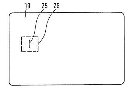
Fig. 6 shows card 19 provided with marking 25 by means of which the proper
positioning of card 19 can be tested. Marking 25 has the form of a hairline
cross and
is disposed in area 26 of the cavity so as not to impair the optical
appearance of card
19. Marking 25 can be provided both on a card in which the cavity is not yet
milled
or is produced in another way, and on a card already having a cavity. In the
latter
case marking 25 is applied to the bottom of the cavity. By the optical testing
station
ascertaining whether marking 25 is present (one-sided testing station) or on
which
side of the card the marking is disposed (two-sided testing station) one can
deter-
mine whether the card is properly positioned with respect to front and back.
Since
marking 25 is applied outside the bisecting lines of card 19 one can
additionally as-
certain whether card 1~> is turned round. Depending on the test result card 19
can be
eliminated or a reversing device can be provided for bringing card 19 into the
de-
sired position.
Besides the above:mentioned applications, the optical testing station can also
be
designed to be able to test the position and/or structure of embossings or
character-
istic printed image elements on the card. Further, it is possible to test the
card mate-
rial, for example with the aid of an infrared or UV detector, for certain
properties, in
particular material properties which are used for later authenticity testing.
In cards in
which a module and/or antenna or other components are integrated into the card
body, it is possible to test the position of the components in transmitted
light or with
the aid of infrared light and also ascertain for example an overlap with the
area of
the cavity or other relevant card elements, such as an embossed area, lasered
area,
etc.
Optical testing of the sheet or of webs from which the cards are later
produced
can be effected both on one side and on both sides. Depending on the kind of
test,
CA 02280721 1999-08-11
-13-
one requires whole-area inspection or only partial inspection, for example of
a se-
lected strip or web. In addition, the optical testing station can also be
provided for
detecting identifications applied to the sheet or webs and passing them on to
the
process control for further evaluation, or applying identifications (e.g.
detected
quality assurance data) to the sheets with a printer (ink jet, etc.) for later
processing
of the data. Moreover, the surface quality of the sheets or webs can be tested
by
suitable measurements of angle of reflection or glancing angle. One can
likewise
determine the sheet or web thickness, and perform different tests with respect
to
flatness, waviness, deformation and edge quality.
The optical testing station can also be designed to be able to test special
prints,
such as fluorescent prints, prints with optically variable inks, iriodine
prints, etc.
Furthermore, it is possible to test not only the position of applied chip
modules but
also the positioning of any desired components, such as magnetic stripes,
signature
stripes and hologram or diffraction structure elements or lens screen
structures.
Altogether one can say that all optical tests necessary for producing card-
shaped data carriers can be performed on the basis of the above invention.
Accord-
ing to the invention these tests are assigned to the corresponding production
steps
depending on their necessity, thereby obtaining fully automatic control of
production
so that rejects rates can be reduced to a minimum while machines can simultane-
ously be optimally utili. ed.