Note: Descriptions are shown in the official language in which they were submitted.
CA 02280732 1999-08-11
WO 98/36466 PCT/US98/03216
ELECTRONIC METHOD FOR CONTROLLING CHARGED PARTICLES
TO OBTAIN OPTIMUM ELECTROKINETIC BEHAVIOR_
FIELD OF INVENTION
This invernion relates to physical, biological, and electrochemical processes
that depend on the
electrokinetic behavior of charged particles, and in particular, an improved
method for controlling
the electrokinetic behavior in such processes.
BRIEF DESCRIPTION OF THE DRAWINGS
FIG. 1 is a perspective plot of the applied emf or electromotive force and the
resulting
charged particle displacement versus time, illustrating one preferred-
embodiment of the
invention.
FIGS. 2A and 2B illustrate waveforms for the applied electromotive force and
the resulting
charged particle displacement with and without a DC onset.
FIGS. 3A and 3B illustrate the electromotive force and resulting displacement
waveforms
when the frequency of oscillation is changed.
FIG. 4 is a plot used to illustrate the three different concepts of reactive
amplification
occurring at system resonance, the effect of damping on circuit transient
response, and the
ability to manipulate the peak amplitude of the injected signal.
FIG. 5 illustrates two alternate waveform emf embodiments and shows both with
positive
and negative DC offset.
FIG. 6 is a system block diagram illustrating the essential elements of the
invention.
FIG. 7 is a simplified system schematic diagram of the one preferred-
embodiment of this
invention.
FIG. 8 is a simplified system schematic diagram illustrating a preferred
alternate-
embodiment.
FIG. 9 is a simplified system schematic diagram of a third preferred alternate-
embodiment
of the invention.
FIG. 10 is a simplified system schematic diagram of an alternate-embodiment of
the
invention
CA 02280732 1999-08-11
WO 98/36466
PCT/US98/03216
FIG. 11 is a perspective drawing illustrating the dynamic nature of the
electrical double
layer at the solid-solution junction and the resulting potential gradient.
FIG. 12 is a perspective drawing of charged particle Brownian movement with
and without
a DC field applied.
FIG. 13 is a perspective plot of activation overpotential versus distance from
the surface to
illustrate the influence of transient concentrations on the reaction rate.
FIG. 14 is a perspective plot of surface charge density versus activation
overpotential to
illustrate the influence of transient concentrations on the surface charge
density.
FIG. 15 is a plot of current versus ion displacement representative of typical
pulsed DC
methods in many prior art processes.
FIG. 16 is a comparative plot of the preferred waveform and resulting
displacement versus
the displacement from an equivalent DC electromotive force.
FIG. 17 is a comparative plot of the preferred waveform versus the pulsed DC
(step
function) waveform described in prior art illustrating the energy loss
resulting from DC.
FIG. 18 gives a plot of an alternate-embodiment emf waveform for high current
applications.
FIGS. 19A and 19B illustrate the electrokinetic behavior of electrons in
flourescent and
phosphorescence materials.
FIGS. 20A and 20B illustrate the structure of a parallel plate capacitor,
dielectric
polarization, and dielectric loss from the application of an alternating
field.
FIG. 21 is an impedance versus frequency plot for several types of battery
systems.
FIGS. 22A and 22B are perspective drawings illustrating the mass-transport
flow in a
plane-parallel electrode system used to compare prior art with the advantages
of this
invention.
FIG. 23 is a perspective illustration of a porous electrode to illustrate the
disadvantages of
using DC electromotive forces and the advantages of this invention.
FIG. 24A is an equivalent circuit for an electrochemical cell and illustrates
the classical
view of a static cell with DC field applied, as described in prior art.
FIG. 24B is an enhanced equivalent circuit for an electrochemical cell
depicting the
dynamic electrolcinetic behavior of the cell when operated as described in
this invention.
FIG. 25 illustrates the effect of the preferred-embodiment waveform on the
electrical
2
CA 02280732 1999-08-11
WO 98/36466 PCT/US98/03216
double layer capacitor.
BACKGROUND OF THE INVENTION
Faraday's Law of Electrolysis explains how the amount of chemical change
produced by the
passage of an electric current is proportional to the total quantity of the
electric charge. Still
Faraday's equation gives only a theoretical value for the change in mass. This
discrepancy is
primarily caused because some charge is consumed in parasitic processes.
A key to electrochemical reaction rates is the ability to manipulate an
additional electrical
potential that results in much greater control of the reaction process. A one
volt change at the
surface of the electrode can result in an eight-order-of magnitude increase in
the reaction rate.
The Butler-Volmer equation expresses the electrode kinetics by relating the
current-overpotential
relationship to the exchange current density and the anode and cathode
transfer coe~cients. For
large overpotential values, a simplification of the Butler-Voliner equation
results in the Tafel
equation:
aQ F
i 1° e~ RT ~s
The Tafel equation can be solved directly to find current density i and
activation or surface
overpotential r)5. The term io is the exchange current, as being the anode
transfer coe~cient, F
is Faraday's constant, R is the universal gas constant, and T is the
temperature in degrees Kelvin.
The potential developed across the cell is equal to:
Y = rls (anode) + rh (anode) + IR - rh (cathode) - rls (cathode)
The term ~~ is the concentration overpotential and the term IR represents the
ohmic losses. The
cathode overpotentials are negative by convention so that the five components
are added to define
the potential across the cell. The five elements are not energy sources and
represent losses.
The reaction rate is dominated by the activation overpotential rls that
results from the
occurrence of an electrical double layer structure that is present at the
solid-liquid (surface-
solution) interface. This electrical double layer or double layer acts as a
capacitor in parallel with
the reaction process. The activation or surface overpotential acts to impede
the electrical field
that is driving the reaction rate. The activation overpotential is a parasitic
energy loss and results
3
CA 02280732 1999-08-11
WO 98/36466 PCT/US98/03216
in the production of heat. Historically, electrochemical systems have been
powered with DC
voltages and currents. Driving the reaction with DC, whether continuous or
pulsed. also means
that a significant portion of the energy is consumed by charging the double
layer.
Stern described the electrical double layer structure as two double layers,
one immobile near
the surface and the other a diffuse region extending into the solution.
Frumkixl added a correction
to the Stern model to account for the changes in the double layer structure
caused by localized
variations in the concentration of the reactants and reaction products.
Stern described the capacitance of the two double layers as two capacitors
connected in series.
The inner or Heliwholtz layer capacitance is designated as Ch and the diffuse
or Gouy-Chapman
layer is designated as Cue. The result of this arrangement is that the smaller
capacitance dominates
the effective capacitance CS (Stern capacitor) of the double layer structure
per the equation:
1 - 1 + 1
CS _ C~ Cs~
FIG. 24B illustrates the electrical circuit configuration. When the Helmholtz
region is highly
concentrated, Cg~ is large compared with Ch so the effective capacitance CS is
approximately equal
to Ch. With a dilute concentration, CS will be approximately equal to Cg~.
FIG. 11 illustrates the theoretical physical arrangement of the double layer
at an active solid-
solution junction. Two lines are drawn on FIG. 11 and labeled by convention as
IHP for inner
Helmholtz plane and OHP for outer Helinholtz plane. The distance from the
surface to the IHP
is roughly one nanometer (nm) and the distance from the surface to the OHP is
about 3 nm. The
typical capacitance developed over this region can be between 10 ~F/cm2 and 50
~F/cmz. If the
potential across the IHP ( 1 nm) is 100 mV then the field strength across the
region is very large
at 1x10⁸ V/m. The potential can be viewed as a kinetic resistance. The
potential energy of an ion
in the electric field is based on the formula ze>Ir, with z equal to the
valence of the ion and a equal
to the charge on the electron. The plane at d coincides with the effective
thickness of the diffuse
layer and can be as small as 3 nm at low concentrations and at fro less than
25 mV. The potential
fro can easily be hundreds of millivolts.
Another important factor is that outside the Helmholtz layer the reactant
species are too
4
CA 02280732 1999-08-11
WO 98/36466 PCT/US98/03216
distant from the surface to react. The significance is that the driving force
for the reaction is the
potential developed across the Helmholtz layer rather than the entire double
layer structure.
FIGS. 13 and 14 are derived from the Gouy-Chapman equations and have
limitations at large
potentials but are useful to illustrate two important properties. As
illustrated in FIG. 13, the
decrease in potential tar, over distance, occurs more rapidly if the
concentration is increasing. FIG.
14 shows that the surface charge density v, for a given potential too,
increases with increasing
concentration.
Other factors control the overall reaction rate. The rate of the electrode
reaction is controlled
by the kinetics of the reaction as discussed. In addition, it is also
dependent on the rate of mass-
transport of reactants and reaction products to and from the reaction site.
The three types of
transport are convection, diffusion, and migration. Diffusion is the process
where particles
disperse from a region of high concentration to a region of lower
concentration. Migration is the
process where a particle moves from one region to another under the influence
of a force, such
as electromigration resulting from the application of an electric field.
A reaction is diffusion controlled if a high probability exists that the two
species will react if
they come into contact. A reaction is activation controlled if the reaction is
highly dependent on
the activation energy of the reaction 'itself. Historically, a system with
mass-transport limits could
be improved with electrolyte agitation. Similarly, high activation energy
barriers were overcome
with the addition of a catalyst or an increase in operating temperature.
When a potential is applied to an electrode, the charges accumulate on the
surface and attract
ions of opposite charge plus molecules that have a dipole moment. FIG. 11
illustrates this action.
For clarity, FIG. 11 does not show the full extent of the presence of the
other molecules and ions
that occupy spaces in the solution. According to the rate equation, a reaction
may slow because
the reactants attempting to reach the reaction site must compete with other
molecules there plus
any reaction products accumulating at the site. Irreversible losses result
from transport limitations
and these factors are responsible for ohmic losses and heating. Vigorous
mechanical stirring of
the solution can increase the rate of mass-transport in such systems.
Nernst defined a diffusion layer thickness 8 (not to be confused with the
double layer effective
thickness) that extends into the solution. The thickness of this layer is a
convenient measure of
CA 02280732 1999-08-11
WO 98/36466 PCT/US98/03216
the resistance of the system to mass-transport of reactants. The thickness of
the diffusion layer
can range roughly 0.01 mm to 0.5 mm. The thickness depends on the system
hydrodynamics,
such that, the thinner the layer the greater the fluid agitation and thus the
better the mass-transport
process. If a process is well stirred, the deposition or dissolution of
material will not affect the
hydrodynamics and thus b.
If the current is increased to a point that the concentration at the surface
approaches zero, a
fizrther increase in current must cause a different reaction to occur (usually
undesired). This limit
defines the limiting current density of a system. The limiting current density
is inversely
proportional to 8. Since the value of b can range 50:1, the limiting current
can vary over the same
magnitude in response to changing conditions in the cell. An electrochemical
system operated at
the limiting current density is operating under mass-transport control.
In a system operating below limiting current density, the rate of the
electrode reaction is the
rate that species are deposited or dissolved as a fimction of the current
density. Current density
depends on the driving force and is greatly influenced by the activation or
surface overpotential
and the concentration of the solution at the reaction site. Again, the
reaction rate is dependent
on the conditions prevailing at the interface. With a high stirring rate and
turbulent flow, the
limiting current density will be higher because the turbulent flow or mass-
transport perturbation
affects the limiting factors. However, for most electrochemical systems,
mechanical stirring is not
practical because of economical or physical restrictions.
Applying an electromotive force to charged particles in a solution will
accelerate the particles.
The velocity of migration of an ion is proportional to the charge or valence
of the ion and the
electric field being applied. As velocity increases friction will increase.
The ion also experiences
a random movement, or Brownian movement, as illustrated in FIG. 12. The
illustration shows the
effects from electromigration. With the application of an external field, the
ion will drift in the
direction of the electric field. In FIG. 12, the ion, without an electric
field applied, starts at point
A and experiences three collisions before ending at point B. With the electric
field applied, the
same ion might start at point A and experience two collisions before ending at
point C. The result
of the electric force is a displacement in the direction of the applied force.
The drift velocity of
an ion is the average velocity in the direction of the applied field. The
vectors shown in FIG. 12
crudely show the result of the collision if the ion had not been under the
influence of the electric
6
CA 02280732 1999-08-11
WO 98/36466 PCT/US98/03216
field: Note that FIG. 12 is a two-dimensional representation in the x and y
plane only and an ion
is free to move in the z plane as well. --
The effective viscosity in the diffuse layer is affected by the application of
the electric field and
the resulting drift or electromigration of the ions in the field. This change
in viscosity results in
an electrophoretic effect or retardation. The retardation causes an ionic
atmosphere to move in
a direction opposite to the motion of the central ion thus reducing the ion's
natural velocity.
Also, the Helmholtz layer is very immobile because the forces are so strong
that the lifetime, in
this layer, of an ion or polarized molecule is long. Any reactant species
entering the double layer
region have to compete for access to the surface. But the electric field
suppresses the reactant
ion's natural three-dimensional Brownian motion. Without the applied electric
force, the ion is
free to move laterally or in a reverse direction until it can find a suitable
reaction site. Suppression
of the Brownian motion can severely limit the ion's ability to move to an
available site. The
combination of these factors contributes to the development of a time lag in
the ion's response
to transient changes in the electromotive force. The result is an increase in
the activation
oveipotential caused by the effects on the double layer structure and an
increase in concentration
overpotential caused by the localized depletions of ions. Depending on the
electrochemical
process involved other negative effects can result, such as parasitic gas
evolution, passivation of
electrodes, dendrite growth, and/or poor electroplating or
electrocrystallization.
The electric mobility a (m2Ns) of an ion is its drift velocity (m/s) in the
field (V/m). The
displacement of an ion under a DC field can be estimated from the equation:
dx=uEdt=uJxdt
The values of a can be found in various chemical reference books. The current
density is
expressed as J and the conductivity as x.
All real systems have at least one resonance point. As the forced response
X(s) at wf
approaches w~ the circuit Q increases. When wf = w", Q is maximum and the
circuit response to
the stimulus is maximum. FIG. 4 illustrates this concept. This important
source of natural
process amplification has been overlooked in the electronic control of
physical and
electrochemical systems.
7
CA 02280732 1999-08-11
WO 98/36466 PCT/US98/03216
Many electrochemical systems depend on the use of a porous electrode. The
porous electrode
can be characterized as a distribution or gradient of reaction rates averaged
over a large structure.
This type of electrode can increase the effective surface area being exposed
for reaction by a
factor of 103 to 105. FIG. 23 shows an illustrative porous electrode.
The previously discussed principles governing reaction rates are applicable to
the porous
electrode but are complicated by the physical structure of the electrode. The
ratio of the electrode
and electrolyte conductivities can vary over the structure so that the current
density is rarely
uniform and is usually highest at the interfaces. The electrolyte permeates
the porous structure
but the problem of localized concentration polarization can be highly
amplified. Non-uniform
current density can lead to localized depletion of reactants and accumulation
of reaction products;
parasitic side reactions; poor material utilization; irregular shaped
deposition; and morphological
changes in the crystal structure. Potential and concentration gradients that
exist promote non-
uniform current density. Because diffusive processes are slow, the porous
electrode is usually
mass-transport limited.
FIG. 23 can help visualize the effect of a long duration DC emf on the porous
electrode. The
ions will be forced to migrate toward the metal current collector for long
periods. As seen, this
makes it di~cult for the hydrated ions to deposit on surfaces that are
parallel to and facing the
current collector. Deposition or electrocrystallization can be poor because
solidification requires
good nucleation and growth but the structure and the applied DC electric field
increase the
chances for poor nucleation. Poor nucleation can result in the formation of
dendrite at the
interfaces.
The localized polarization problems have been recognized for a long time and
many techniques
have been developed to limit the undesired polarization. It is well-known that
using pulsed DC
improves the e~ciency of electroplating. The theory is that the pulse is
applied for a duration of
time that is shorter than the time it takes for any significant concentration
polarization to develop.
Since at least the laze 1960's, it has been well-known that using pulsed DC
improves the
charging e~ciency of batteries. The widely distributed and highly acclaimed GE
Nickel-Cadmium
Battery Application Engineering Handbook outlines these techniques. Since
then, many US
Patents have been issued for various techniques that use pulsed DC techniques
to improve the
CA 02280732 1999-08-11
WO 98/36466 PCT/US98/03216
charge efficiency.
Noteworthy, earlier US Patents include, 3,597, 673 and 3,614,583 issued to
Burkett et al and
3,617,851 issued to Du Puy et al. The inventions in these patents apply a
continuous or pulsed
DC charge with a relatively long duration followed by a discharge pulse (load)
of short duration.
The discharge pulse is applied to depolarize the battery. The primary
difference between the
inventions is the frequency and duration of the applied pulses. US Patent
number 4,385,269,
issued to Aspinwall et al, described a pulsed DC charge followed by a
depolarization pulse and
a second technique of applying a two-tier pulsed DC charge followed by a
depolarization pulse.
The duration of the charge pulse was about ten seconds and the depolarization
duration was
roughly two seconds. In US Patent number 4,746,852, issued to Martin, the 1
second pulsed DC
charge was followed by a 5-millisecond depolarization pulse. The charge and
depolarization
pulses were then followed by a 15-millisecond measurement period. US Patent
4,829,225, issued
to Podrazhansky et al, introduced a pulsed DC charge of 0.1 to two second
duration followed by
a depolarization pulse of 0.2 to S percent of the duration of the charged
pulse. The charge and
depolarization pulse was followed by a rest period that exceeded the duration
of the
depolarization pulse. The rest period was further defined as an ion
stabilization period of about
7 to 20 milliseconds. It was claimed that the rest period had beneficial
results by allowing the ions
to find their position between the battery plates. In US Patent number
5,307,000, issued to
Podrazhansky et al, a single or double DC pulse with rest period was followed
by a plurality of
depolarization pulses with rest periods. It was claimed that the discharge
pulses served to create
and disperse ions throughout the electrolyte. Multiple depolarization pulses
were used so that
natural chemical and electrical gradients within the battery would also serve
to disperse the ions
more evenly. The charge pulse had a duration of at least 150 milliseconds, the
depolarization
pulses had a duration roughly 0.4 percent of the charge pulse, and the waiting
periods varied over
a range of 0.4 to 2.4 percent of the charge pulse. A fiurther claim described
how the high
discharge current would cause the diffusion layer to break up and the waiting
period allowed time
for the ions to migrate away from the plate. This action caused the plate to
be more receptive to
a high charging current pulse.
One common attribute and problem with prior art is the dependence on DC,
whether
continuous or pulsed. The major advantage claimed, in all of the inventions
discussed, is an
9
CA 02280732 1999-08-11
WO 98/36466 PCT/US98/03216
improved method-of or result-from applying depolarization pulses. FIG. 15
illustrates a
waveform typical of prior art inventions. The use of DC causes a polarization
overpotential to
develop that reduces the charge acceptance and this polarization must be dealt
with to achieve
reasonable charge acceptance. The overpotential that develops is a combination
of activation and
concentration overpotentials. Remember that an overpotential is a deviation in
the electrode
potential necessary to cause a given reaction. The losses that result are
irreversible and lead to
the generation of heat. All of the prior art processes cause a polarization
build-up.
The DC pulses descnbed can be analyzed as a DC step function. A Fourier
analysis of an ideal
step function would yield harmonics out to infinity. In practical circuits,
the step functions are
far from ideal but the rise times are very fast and the harmonic energy
generated extends to very
high frequencies. A time-frequency domain transformation reveals that the
continuous spectrum's
envelope extends to the corner frequency f, = 1/~i, with pulse width z. For a
100-nanosecond
rise time t~ the 2"° corner frequency fz would be about 3 MHz. The
envelope amplitude decreases
after f, at the rate of -20 dB/decade and -40 dB/decade after f2.
Experimentation reveals that ions
have a transient response time on the order of 1 to 10 microseconds. Various
measurement
methods can determine this value and FIG. 21 illustrates one method. FIG. 21
is a plot of the
impedance versus frequency, plotted on a log-log scale, for several types of
batteries. A pulse can
rise faster than the ions can deliver the charge. If a pulse's rate-of rise
exceeds the ions' transient
response time, the system must (by definition) be mass-transport limited.
Under this condition,
the limiting current density is momentarily exceeded and the energy in the
pulse must be
converted to heat by some undesired process.
As stated earlier, each application of pulsed DC charges the double layer
capacitor on the
leading edge and discharges it on the falling edge. FIGS. 20A and 20B show the
physical
structure of a parallel plate capacitor. The capacitance developed by a
parallel plate capacitor is:
C - E A
d
The permittivity of the dielectric is represented by E, the plate area by A,
and the distance between
the plates as d. From the equation the capacitance is obviously directly
related to the permittivity
of the dielectric. In a double layer capacitor, the polarized water dipoles
form the dielectric
CA 02280732 1999-08-11
WO 98/36466 PCT/US98/03216
material FIG. 11 shows the structure of the electrode-electrolyte junction
that forms the double
layer capacitor and the physical relationship of the water dipoles to the
electrode.-~n a liquid the
dipoles are easily polarized. In the IHP, the surface charge causes the
dipoles to be highly
polarized. However, in the OHP the dipoles are more highly influenced by the
ions than the
surface charge. If the concentration of ions increases, the dielectric
constant (permittivity)
decreases thus the capacitance decreases. Likewise, if ion concentration
decreases then
capacitance increases. The current required to charge the capacitance with DC
follows the
equation:
i =C dV
dt
The energy required to charge and discharge the double layer capacitor is
wasted since it does not
contribute to the electrochenucal reaction. Because of the overpotentials that
result, the
application of DC pulses can reduce the effective reaction rate.
FIG. 24A shows an equivalent circuit for a typical battery cell and is
compatible with the
equivalent circuit described in the GE Nickel-Cadmium Battery handbook and
other battery texts.
A double layer structure will form at the solid-solution interfaces in an
electrochemical system
under the influence of an electromotive force. In one time constant Cp would
be charged to 63.2
or discharged to 36.8% of its final value. Charging a cell with a pulse
duration on the order
of one time constant and a short duration discharge pulse will charge the
capacitor in a little more
than 5 times constants. The depolarizing pulses slightly discharge the
capacitor. The wait periods
allow the ions outside the Helmholtz region to di$use freely but the potential
across the region
holds the double layer structure essentially intact. The combination of short
duration
depolarization pulses and wait periods (less than S time constants) have
little effect on the
structure of the double layer capacitor and the activation overpotential that
develops.
Depending on whether the cell is operating as an electrolytic or galvanic
cell, the double layer
structure at one electrode will dominate the overall reaction. If a particular
electrode dominates
the reaction with current flowing in a given direction then the other
electrode dominates when the
direction of current is reversed. With few exceptions, cations do not enter
the inner Helmholtz
plane because of Gibbs free energy restrictions. This fact means that the
dielectric constant is
11
CA 02280732 1999-08-11
WO 98/36466 PCT/US98/03216
very high and the capacitance is therefore very large. The effective
capacitance of the cell is
therefore dominated by the opposite electrode with the smaller capacitance.
Claims that the
depolarization pulses and wait periods breakup or eliminate the double layer
ignore the physics
of the structure.
Battery chargers that use i20 Hz rectified DC pulses, typical of the 1960's
and as described
in the GE Nickel-Cadmium handbook, are effectively pulsed DC to the double
layer capacitor.
The rest or offperiods are of longer duration than newer technologies but
short enough that the
capacitor reaches full charge in a short time. However, the rest periods are
of su~cient duration
that they waste significant energy in the charge and discharge of the double
layer. Because the
rest period is of relatively short duration, the measurement of the 'trough'
voltage during the off
period is not the true open-circuit voltage of the cell, as often claimed. The
newer techniques,
discussed above, suffer because the rest periods are too short, compared with
the time constant
of the capacitance, to discharge the overpotential. The measurements are free
from the
instantaneous 'IR' losses associated with the concentration overpotential but
still have an
overpotential error.
An additional problem with long duration DC is the ionization of water at the
electrodes as
a parasitic side reaction. F'IG. 11 shows the water dipole's relationship to
the positive electrode.
The longer the DC potential holds the water dipole tightly to the surface the
greater the chance
that the water will dissociate into H', O-z, and OH . Because of the strong
attraction. oxygen may
adsorb at the positive electrode and hydrogen may be adsorbed at the negative.
The remaining
elements (by-products) may impede the overall reaction or cause other problems
such as gas
pressure build-up.
As discussed, when the DC pulse duration is long, compared with the transient
response time
of the ions, the process can be analyzed as continuous DC. It is well-known
and documented that
transient response techniques can be applied to electrochemical systems to
separate out the
various overpotentials for individual analysis and measurement. Other than
pulsed DC, techniques
that take advantage of the ion's natural transient responses have not been
applied to
electrochemical processes to optimize the overall reaction rate.
A battery is an example of an electrochemical system that can be used in
either an electrolytic
12
CA 02280732 1999-08-11
WO 98/36466 PCT/US98/03216
(energy consuming) or galvanic (energy producing) process. Batteries are often
charged with
pulsed DC and a depolarizing pulse. The application of the depolarizing
(energy consuming)
pulses momentarily converts the battery to a galvanic cell but the intended
operation is an
electrolytic process. Except as noted, transient response techniques are used
to improve the
reaction rates for electrolytic processes but not for galvanic processes.
Battery packs (multiple cells) often integrate a control circuit, such as a
microprocessor, into
the pack to monitor the battery's charge and discharge cycles. US Patent
4,289,836, issued to
Lemelson, integrated a microprocessor into a pack for sensing and controlling
the battery
charging. The control circuitry usually monitors the current entering or
leaving the battery. The
control may combine the charge and discharge current with an estimate of self
discharge,
including a temperature compensation factor, to predict the available charge
capacity of the pack.
Additionally, charge termination can be made via the control circuit by
sending a control signal
to the external power source to terminate charge. In more complex
applications, the internal
control circuitry communicates with an external programmable power supply via
a serial bus. US
Patent 5,572,110, issued to Dunstan, describes this type of system. The
control can specify the
power supply's current and voltage levels to match the battery chemistry. This
last technique
allows the prograrmnable power supply to be safely used with various battery
chemistries. In US
Patent 5,471,128, issued to Patino et al, a battery undervoltage protection
circuit is described.
US Patent 5,569,550, issued to Garrett et al, overvoltage protection for the
battery is added. In
US Patent 5,218,284, issued to Bums et al, a switching power supply is
included to control both
the charge and discharge current levels. Except as noted, the control
circuitry does not actively
enhance the discharge perfom~ance of the battery in a galvanic mode of
operation.
All battery systems experience the problems of voltage depression (memory) and
self
discharge. The severity of the problem is different from system to system and
varies significantly
with operating conditions. One major cause is morphological change in the
crystal structure.
These changes primarily occur in areas of the crystal where the material has
been inactive. When
the material is inactive for extended periods, the crystal structure can
change size. When this
change occurs, the material becomes less active and is not available to
contribute to the reaction.
Long-term storage and shallow discharge followed by taper charging results in
areas where the
material is inactive for long periods. The inactive material can be
conditioned and restored by the
13
CA 02280732 1999-08-11
WO 98/36466 PCT/US98/03216
application of several deep discharge/charge cycles. The problem is deep
discharge cycles are
detrimental to the operational life on all battery systems. Conditioning is
time consuming and
generally unavailable. The problem with self discharge is that the battery is
not available on-
demand without recharging or a special maintenance program to test
periodically, possibly
condition, and recharge the battery.
Charge transfer occurs several ways. Electrons transfer the charge in metals
and
semiconductors whereas ions transfer charge between a metal and a solution of
its ions. The three
forms of transmission are electron flow, ion flow, and charge transfer
reactions at the electrode-
electrolyte interface. The equations relating the charge transfer steps of
ions and electrons are
very similar.
Two systems that rely on electron charge transfer are illustrated in FIGS. 19A
and 19B. These
systems have historically relied on an alternating current electromotive force
to provide activation
energy. A flourescent system is shown in FIG 19A. In this system, the valence
band and
conduction band are separated by an energy gap, shown as Eg When a stimulus is
applied, an
electron gains sufficient energy to jump to the conduction band. Obeying the
natural tendency
to return to the lowest energy level available, the electron gives up the
extra energy and drops
down to the valence band. In the process a photon is emitted. The wavelength
of the light
emitted depends on the width of the energy gap. In this situation, the
wavelength is emitted in
the visible band so useful light results. The emission of light stops when the
electrical stimulus
is removed. Increasing the frequency of the applied ac waveform increases the
frequency that
Light is emitted and effectively increases the light output. The problem with
prior art is that the
control circuitry that provides the most efficient light output is much more
expensive than the less
e~cient but cheaper 60 Hz control circuitry. A primary reason for the high
cost is the complex
circuitry needed to produce the higher frequency (40 kHz) ac waveform. Dimming
can save
additional energy when applicable but the additional circuitry cost is
prohibitively higher.
A phosphorescence system is shown in FIG 19B. Again, an energy gap separates
the valence
and conduction bands. An additional energy level, shown as E~, results from
the introduction of
a donor (impurity) into the material. When the electrical stimulus is applied,
the electron gains
the necessary energy to jump to the conduction band. When the electron drops
back down, it
emits a photon but then becomes trapped in the donor trap level. The electron
will remain in the
14
CA 02280732 1999-08-11
WO 98/36466 PCT/US98/03216
donor trap level temporarily before dropping back to the valence band. A
photon will be emitted
when the electron leaves the donor trap level. Because the electron is
temporarily trapped in
donor trap level, the phosphorescent material will continue to emit light for
a short time after the
electrical stimulus is removed. Historically, this type of system has been
powered with complex
ac power sources.
One phosphorescent light system of interest is the electroluminescent lighting
strip. The light
output e~ciency of the strips is low and they can experience short operational
life. Increasing the
ac voltage's amplitude (up to 380 Vans) and frequency (up to 8 kHz) can
increase the light
output. The conflict is that the operational life is inversely proportional to
the ac voltage's
amplitude and frequency. The physical structure of the material is similar to
a parallel plate
capacitor so that the impedance of the system is largely capacitive. Low-cost
inverters are
available for powering small strips, up to 20 VA. The technology for producing
very large or
very long strips is now available. However, the cost of 150 VA to S00 VA ac
power supplies is
prohibitively high and is hindering the acceptance of the systems. FIG. 20 is
an illustrative
drawing of a dielectric system similar to the electroluminescent strip.
Current texts on the subject
explain that the electroluminescent strips cannot be driven with DC and the
upper operating range
for ac is 8 kHz. As shown in FIG. 20, the application of an electromotive
force polarizes the
molecular dipoles in the dielectric material. If the potential is reversed as
occurs with alternating
current, the molecular dipoles must reverse 180°. The rotation
introduces a dipole-friction and
a displacement current flows. The result is that the dielectric loss increases
with frequency.
Molecular dipoles experience the highest dielectric loss at roughly 10 kHz.
Corona discharge is
a problem at the present levels of ac voltage. The corona can cause the
plastic insulating materials
to deteriorate rapidly. Being able to control the light output is highly
desirable but the cost of
dimming circuitry for the larger strips is prohibitively high.
OBJECTS AND ADVANTAGES
Accordingly, it is an object of this invention to provide an electromotive
force (emu that
effectively utilizes the natural resonance or other physical properties of a
system to optimize the
electrokinetic behavior of the charged particles, and further, utilizes the
reactive energy or
CA 02280732 1999-08-11
WO 98/36466 PCT/US98/03216
amplification at resonance to increase the effectiveness of the process
without an increase in the
applied input average or DC power.
Additionally, it is an object of this invention to match the shape of the
input stimulus' waveform
(emu to optimize the charged particles' natural movement or behavior, in
particular, to normalize
the input stimulus' amplitude and frequency to match the relative interactions
between the
charged particles and the physical structure of the process. As examples, the
emf should
maximize the natural Brownian movement of an ion and the prevailing diffusion
process in a
solution. The displacement, in time, of ions should be normalized to the
physical distances of the
electrical double layer.
An object of this invention is to produce an electronic catalytic effect in an
electrochemical
process by effectively reducing the activation overpotential, concentration
overpotential. and
energy loss in the electrical double layer thus reducing the activation energy
needed for the
reaction to occur. Further, it is an object of the electronic catalytic effect
to increase the exchange
current in the system's process thereby increasing the limiting current
density with the result being
an improvement in efficiency and throughput for the process.
An object of this invention is to provide an electronic method for providing
mass-transport
perturbation, especially including the electrical double layer, and further,
to create an
electromotive perturbation that is perpendicular to the electrodes that
optimize the natural
processes of Brownian movement, diffusion, and convection. Further, it is an
object of the
perturbation to optimize the concentration of reactants at the reaction sites
and reduce the
development of concentration gradients over the surface while maximizing the
penetration within
the porous electrodes, if applicable, thereby increasing the effective surface
area of the electrodes.
Still further, it is an object of the perturbation to improve the
electrodissolution, electrodeposition,
or electrocrystallization at the surfaces.
An object of this invention is to provide a process that utilizes the
impedance of an active
electrochemical system to control the amplitude of the applied emf and
particularly, to allow the
system impedance to naturally damp the amplitude of the applied electromotive
force thereby
allowing automatic process control of the emf amplitude. Still further, it is
an object to adjust the
DC offset, peak currents, duty-cycle, and frequency of the control process to
match the changing
16
CA 02280732 1999-08-11
WO 98/36466 PCT/US98/03216
conditions of the system.
It is an object of this invention to avoid DC polarization thus eliminating a
need for a
depolarization pulse and thereby reducing the additional parasitic effects of
the DC and
depolarization pulse.
It is an object of this invention to obtain true open-circuit voltage and
accurate closed-circuit
voltage measurements during an active electrochemical process. Further, the
improved voltage
accuracy will increase the accuracy of coulometric measurements of charge,
discharge, or self
discharge occurring in the system.
It is an object of this invention to provide an emf for battery charging that
reduces the production
of heat and overpotential thereby allowing simple voltage and temperature
measurements to
detect full-charge reliably and accurately. Additionally, the fast and
reliable detection will avoid
damaging overcharge, particularly, with high-C rate charging. Further, it is
an advantage of the
simple, fast, and reliable detection (of full charge) that high-C rate
charging can be maintained
until full-charge is reached, without protective current tapering. Still
further, it is an advantage
of the improved accuracy of voltage measurement and reliable detection of full-
charge that safe
higher rates of charging are possible.
An object of this invention is to provide process control, via transient-
response and integral-
transform techniques, that can be used to improve the reaction rate of both
electrolytic and
galvanic systems, and in particular, to provide a method that can be used to
control battery
performance during both electrolytic or galvanic modes of operation.
It is an object of this invention to provide a method for providing a control
circuit (module) that
can be integrated into a battery pack (multiple cells) to control both the
electrolytic and galvanic
modes of operation. Further, it is an object of this invention that the
geometric shape and size of
the module will be roughly equivalent to the space occupied by one cell in a
multiple-cell pack.
Still further, it is an object of the control module to contain active
circuitry for controlling: (a) the
input and output current; (b) regulation of output voltage; and (c) charge and
discharge of the
battery, including temperature compensation. It is an advantage of this
invention that the personal
safety of the pack user increases with active short-circuit and overcharge
current protection and
further the improved charge and discharge performance maximizes the
operational life of the
17
CA 02280732 1999-08-11
W0 98/36466 PCT/US98/03216
battery pack. An additional advantage is the overall reduction in system cost
since an external
battery charger will no longer be required and a low-cost, unregulated power
supply can be used.
It is an object of this invention to provide an emf waveform that promotes the
benefits of thicker
electrodes without a loss of peak current capability.
It is an object of this invention to provide a process to exercise a battery
during storage or periods
of inactivity to reduce the effects of inactive material and self discharge.
It is an object of this invention to provide a modified (alternate-method) emf
waveform that offers
many of the preferred waveform's benefits but is better suited for very high
current applications.
A further object of this invention is to provide a low-cost process for
powering luminescent
systems that provides low-cost circuitry for dimming, and particularly in
electroluminescent
lighting systems, a DC emf waveform that: {a) effectively eliminates
dielectric loss; (b) reduces
corona discharge; (c) extends the operational frequency limit above 8 kHz; (d)
increases output
brightness; and (e) extends the operational life.
It is an object of this invention to provide safety, environmental, and
economical benefits.
Advantages include: (a) improved personal and system safety; (b) less energy
consumption; (c)
better material utilization; {d) reduction of electromagnetic interference
(EMI) by eliminating high
frequency harmonic energy; (e) tighter process control; (f) simpler circuitry;
(g) lower costs; (h)
longer operational life; and (i) higher throughput.
Further objects and advantages of the invention will become apparent from a
consideration of the
drawings and description that follows.
SLTMMARY OF THE INVENTION
An electronic method is provided whereby the applied electromotive force
optimizes the
electrokinetic behavior of charged particles to match the natural electrical
response and physical
structure of the system. Electrokinetic behavior is the resulting charged
particle motion caused
by changes in the applied electric field. This method can be applied to a very
broad field of
applications that include physical, biological, and electrochemical systems,
such as, electrolysis,
18
CA 02280732 1999-08-11
WO 98136466 PCT/US98/03216
batteries, and ffourescent and electroluminescent lighting (photochemical)
systems. This method
can be applied to batteries to improve both electrolytic and galvanic modes of
operation. An
unexpected benefit of the method is that the circuitry needed to provide the
optimized
electrokinetic behavior is lower in cost than the existing circuitry.
DESCRIPTION OF THE PREFERRED EMBODIMENTS
FIG. 1 illustrates an electromotive force (emf) of the method that produces a
desired charged
particle displacement for optimized electrokinetic behavior. The emf takes the
shape of an ideal
damped sinusoidal waveform superimposed on a DC potential. Practical
implementations of this
method will deviate from the ideal shape shown. The waveform takes the form:
emf = f(x) + h(x)
The function f(x) is the sinusoidal wave with exponential decay and takes the
form:
,f(x) = AXexp_~ B~ Xsin(Cxx)
The value A establishes the amplitude, B defines the rate of decay, and C sets
the frequency of
oscillation. The function h(x) defines the offset and takes the form:
h(x) = Dx atan(Rxx)
Value D is an offset multiplier and value R sets the rate of approach to the
offset.
In FIG. 1, a first positive peak causes an initial positive displacement of
the charged particle.
As the waveform approaches the zero point, the slope of the displacement
approaches zero. As
the waveform continues the potential becomes negative and the charged particle
displacement also
becomes negative. The negative displacement is roughly 1/3 of the initial
positive displacement.
As the emf waveform again approaches zero potential, the slope of the charged
particle
displacement again approaches zero. At a second peak, the emf continues to
increase positively
and the displacement again becomes positive. The positive displacement of the
2"d positive peak
is roughly 2/3 of the initial first positive displacement. As the emf
approaches zero potential, the
19
CA 02280732 1999-08-11
WO 98/36466 PCT/US98/03216
slope of the charged particle displacement approaches zero for a third time. A
second negative
emf peak causes a negative charged particle displacement that is roughly 1/3
of the positive
displacement caused by the second positive emf peak. This process continues
for one more
oscillation cycle. As the emf waveform is reduced or damped the resulting
charged particle
displacement is also reduced. FIG. 1 shows one process cycle with three
oscillation cycles. At
the end of the third oscillation cycle, at time = 60, the process cycle would
begin again.
FIGS. 2A and 2B depict the effect of a DC offset on a damped sinusoidal emf:
The emf
waveform follows the fom~at described for FIG. 1. FIG. 2A shows a damped
sinusoidal emf with
no DC offset. A positive net displacement will result because the emf's
leading positive peaks
have greater amplitude than the following negative peaks. FIG. 2B shows a
damped sinusoidal
waveform with a DC offset applied that is similar to FIG. 1 but with different
peak amplitudes.
FIG. 2A shows greater negative charged particle displacement per unit of time
than FIG. 2B.
FIG. 2B shows roughly a 5 to 1 increase in net positive displacement per unit
of time than FIG.
2A.
FIGS. 3A and 3B show two damped sinusoidal waveforms with identical peak
values and DC
offset but operated at different frequencies of oscillation to illustrate the
effect on charged particle
displacement. FIG. 3A shows an emf at base ( 1 x) frequency and a resulting
charged particle
displacement in time. FIG. 3B shows an emf at twice the base frequency and a
resulting charged
particle displacement in time. For comparison purposes only, FIG. 3B shows
roughly 6 oscillation
cycles but in a practical application a second process cycle would begin at
time = 50. The
comparison illustrates that increasing the frequency of oscillation results in
a decreased
displacement in time.
FIG. 4 shows a damped sinusoidal waveform with different peak amplitudes.
FIG. 6 shows a block diagram of the essential elements needed to implement
this method.
System 50 consists of injection-means 1, waveform-generator 2, control-circuit
3, process 4,
power-source 5, and control-signals 6, 7, and 8. Process 4 is the physical
process to be
optimized. Injection means 1 couples the outputs from waveform-generator 2 and
power-source
then supplies the resulting emf to process 4. Waveform-generator 2 is a
conventional
waveform generator used to develop the emf signal supplied to injection-means
1. Control-circuit
CA 02280732 1999-08-11
WO 98/36466 PCT/US98103216
3 generates control-signal 6 to control the output of waveform-generator 2.
Control-circuit 3 is
conventional in implementation and can be as simple as an operational
amplifier circuit or as
complex as a microcontroller or full computer system. Power-source 5 is
conventional and could
range from the ac mains to a programmable power supply.
Control-signal 6 can be a single signal or a plurality of signals, including
voltage, current,
frequency, duty-cycle, and/or damping ratio, used to control the output from
waveform-generator
2. Control-signal 7 can be a single signal or a plurality of signals and can
be unidirectional or
bidirectionaL Control-signal 7 can be used by control-circuit 3 to monitor
and/or control process
4 directly. Control-circuit 3 controls process 4 indirectly via waveform-
generator 2, injection-
means 1, and (possibly) power-source 5. Control-circuit 3 could control
certain parameters of
process 4, such as temperature, directly via control-signal 7. Control-signal
7 can be used as
process feedback from process 4 for voltage, current, impedance, temperature,
pH (hydrogen-ion
activity), pressure, and/or other statistical process control (SPC) parameter.
Control-signal 7 is
optional if system 50 is operated open-loop (without feedback from process 4).
Control-signal
8 is used optionally by control-circuit 3 to monitor and/or control power-
source 5. Control-signal
8 can be a single signal or a plurality of signals and can be unidirectional
or bidirectional. Control-
signal 8 could be used to control the output parameters of voltage, current,
and frequency from
power-source 5.
FIG. 7 is a simplified schematic diagram of system 51 derived from the block
diagram in FIG.
6. System 51 consists of the same essential elements described in system 50.
Control-circuit 3,
process 4, power-source 5, and control-signals 6, 7, and 8 are identical in
function and description
to system 50. Injection-means 1 is fiurther clarified in FIG. 7 as a coupled-
inductor 9. The circuit
symbol for coupled-inductor 9 is unfortunately identical to the symbol used to
identify a
transformer. The construction and operation of coupled-inductor 9 are very
similar to a
conventional transformer. For discussion purposes, the primary winding
(injection winding) of
coupled-inductor 9 is connected between process 4 and power-source 5 while the
secondary
is connected to waveform-generator 2. The main distinction between coupled-
inductor
9 and a transformer is the importance of the inductance in the winding. The
primary winding of
coupled-inductor 9 must act as a current-source (inductor) to match the
impedances of power-
source 5 and process 4. Although not shown, an essential feature for proper
operation of
21
CA 02280732 1999-08-11
WO 98/36466 PCT/US98/03216
coupled-inductor 9 is the inclusion of a capacitor in the output of power-
source 5. This capacitor
completes the current path for the primary winding of coupled-inductor 9 and
process 4 through
system 51 ground.
Waveform-generator 2 is shown in FIG. 7 to consist of switch 12, inductor 11,
capacitor 10,
and diode 13. Waveform-generator 2 in system 51 is a conventional LC-tuned
oscillator.
Control-signal 6 activates switch I2 to initiate an oscillation cycle.
inductor 11, secondary
winding of coupled-inductor 9, capacitor 10, and diode 13 form a conventional
LC tank circuit
used to generate the desired emf waveform. The waveform developed on capacitor
10 is applied
directly to the secondary winding of coupled-inductor 9. Coupled-inductor 9
superimposes
(couples) the emf waveform from the secondary winding onto the DC current
supplied by power-
source 5. Switch 12 is shown as a pnp transistor but can be any switch
suitable for the
application.
DESCRIPTION OF ALTERNATE EMBODIMENTS
ADDITIONAL EMBODIMENT DESCRIPTION FOR EMF WAVEFORMS
FIGS. SA, SB, SC, and SD show four different but similar emf waveforms. FIGS.
SA and SB
waveforms take the form:
f(x) _ ( - ~ (sin(x-c)) ~ + DC offset) peak emf
FIG. SA shows the waveform with a positive DC offset and FIG. SB shows the
waveform with
a negative DC offset. The FIGS. SC and SD waveforms take the form:
fix) _ ( ~ (sin(x-c)) ~ + DC offset) peak emf
FIG. SC shows the waveform with a positive DC offset and FIG. SD shows the
waveform with
a negative DC o~et. Practical implementations of this method will deviate from
the ideal shapes
shown.
ADDITIONAL EMBODIIvvIENT DESCRIPTION FOR HIGH CURRENT EMF WAVEFORM
FIG. 18 shows an emf waveform developed from a current-source with a limited
rate-of rise.
Practical implementations of this method will deviate from the ideal shape
shown. This alternate
22
CA 02280732 1999-08-11
WO 98/36466 PCT/US98/03216
waveform is a modified pulsed DC emf. The current is camped from the 0 value
to a positive
peak value at a rate-of rise that matches the operational performance needed.
The positive
amplitude is maintained at the positive DC rate for a specified time. The
current is then camped
down at a controlled rate until the negative peak is reached then the current
is reversed and
camped back to the positive peak value. The percentages of time are shown as a
reference and
can be adjusted to match the application. Likewise, the dwell time at zero
crossing is shown as
zero but it could be set for a period greater than or equal to 5 time
constants. The example shown
is based on 50 cycles of 60 Hz ac power and the ramp time from one peak to the
other peak being
equal to 8.333 milliseconds.
ADDITIONAL EMBODIMENT DESCRIPTION FOR INJECTION-MEANS
FIG. 10 shows system 54 with an alternate circuit implementation for injection-
means l and
waveform-generator 2. Control-circuit 3, process 4, power-source 5, and
control-signals 6, 7,
and 8 are identical in description and operation as system 50. The functional
operation of system
54 is identical to the descriptions given for system 50 with the exception
that injection-means 1
is implemented as a conventional linear amplifier circuit and waveform-
generator 2 is implemented
as oscillator 32. Oscillator 32 is a conventional circuit used to generate
either a sinewave,
triangular, or squarewave signal. The output of oscillator 32 is supplied to
switch 31. Switch 31
is shown as a npn transistor but can be any switching device suitable for the
application. Although
not shown, the output of oscillator 32 would normally be capacitively coupled
to the base of
switch 31. Resistors 27 and 28 are used to set the Q point for switch 31.
Resistor 29 is an
emitter resistor used to generate feedback to control the stability of switch
31. Resistor 30 is the
collector resistor used to control the current for switch 31.
ADDITIONAL EMBODIMENT DESCRIPTION OF INTEGRAL BATTERY MODULE
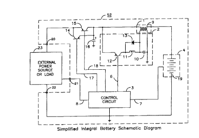
FIG. 8 shows module 52 and external-circuit 23 that comprise the essential
elements described
in system 50. Module 52 consists of injection-means l, waveform-generator 2,
control-circuit
3, process 4, switches 14 and 15, capacitor 16, connections 20, 21, and 22,
and control-signals
6, 7, 8, 17, and 18. Injection-means 1 and waveform-generator 2 are shown in
detail for clarity
and are identical in function and description as given in system 50. Process 4
is fiu~ther defined
as battery 19. Capacitor 16 is an essential element for the proper operation
of coupled-inductor
23
CA 02280732 1999-08-11
WO 98/3b466 PCT/US98/03216
9 with the addition of switches 14 and 15. Capacitor 16 completes the current
path for the
primary winding of coupled-inductor 9 and battery 19 through module 52 ground.
Control-circuit
3 is identical in function as given in system 50 but in module 52 the function
is better defined than
the global description given in system 50. Control circuit 3 is normally
implemented with a
microcontroller integrated circuit. Control-signals 17 and 18 control the
direction of current
flow, via either switch 14 or switch 15, for external-circuit 23, coupled-
inductor 9, and battery
19. Control-signal 18 is used to charge battery 19 via switch 15 and control-
signal 17 is used to
apply power to external-circuit 23 via switch 14. Switches 14 and 15 are shown
as pnp
transistors but any switch could be used that is suitable for the application.
Switch 15 may also
be a diode if control of charge is not desired or necessary. The collector of
switch 14 and emitter
of switch 15 are shown tied to connection 20 but optionally switches 14 and 15
could be wired
separately to external-circuit 23. Although not shown, voltage feedback would
be supplied from
connection 20 and capacitor 16 to allow control circuit 3 to detect the
presence of external circuit
23 and the voltage level at capacitor 16. Control-circuit 3 monitors the
condition of battery 19
through control-signal 7. In module 52, control-signal 7 can be a single
signal or a plurality of
signals that include measurements of voltage, current, impedance, temperature,
and pressure from
battery 19. Control-signal 6 is identical in function and description as given
in system 50.
External-circuit 23 can be either an external power-source similar to power-
source 5 or an
external system that operates from the power developed by battery 19. Control-
signal 8 is
optional. Control-signal 8 can be a single signal or plurality of signals and
can be unidirectional
or bidirectional. Control-signal 8 may be used to control the output of
external-circuit 23 when
it is a programmable power-source or to communicate with external-circuit 23
if applicable.
Connections 20, 21, and 22 are connection points shown to emphasize the
difference in module
52 and system 51.
ADDITIONAL EMBODIMENT DESCRIPTION OF INTEGRAL BATTERY MODULE
FIG. 9 shows module 53 that is essentially identical to module 52 except for
the addition of
inductor 24, capacitor 25, and diode 26. Switch 14, inductor 24, capacitor 25,
anti diode 26 are
configured as a switching power supply. Control-signal 17 is now a pulse-width-
modulator
(P~ control signal to control the duty-cycle of switch 14. Control-signal 8
must include the
function of feedback for proper regulation of the output voltage at connection
20. Although not
24
CA 02280732 1999-08-11
WO 98/36466 PCT/US98/03216
shown, feedback would be provided from connection 20 to control-circuit 3 with
or without
external-circuit 23 being connected at connections 20, 21, and 22. This
configuration allows
control-circuit 3 to provide a fixed or programmable output voltage at
connection 20. External-
circuit 23 can provide a programming signal, at connection 2 i, via a serial
bus communication or
a simple voltage or resistance setting. The config~untion shown (buck) can
only provide a voltage
that is less than the voltage of battery 19. Alternately, the components of
switch 14, inductor 24,
capacitor 25, and diode 26 can be rearranged (buck/boost) to provide a voltage
greater or equal
to the voltage on battery 19. Switch 15's emitter is again shown connected at
connection 20 but
it could be wired separately. Although very diffcult to implement because of
the conflicting
requirements, coupled-inductor 9 could also be used to form the switching
power supply. Switch
14 would be connected with the emitter to coupled-inductor 9 and the collector
to the positive
electrode of battery 19. Diode 26 would be connected to the emitter of switch
14 and module
53 ground. Inductor 24 and capacitor 25 would be eliminated. In this
configuration switch 14,
coupled-inductor 9, capacitor 16, and diode 26 would form the switching power
supply. Switch
15 could be a diode connected in parallel with switch 14 to allow charging
current to bypass
switch 14.
THEORY OF OPERATION
Physical and electrochemical systems have naturally occurring electrical
characteristics that
govern the efficiency and effectiveness of the particular processes involved.
The characteristic
of interest to this method is the electrokinetic behavior of the charged
particles. Although not
within the scope of this invention, the first process necessary to optimize
the electrokinetic
behavior of the charged particles is a thorough understanding of the process
to be controlled.
This understanding requires a detailed analysis of the transient response
behavior, including
evaluation of the transfer functions for the time-domain and the integral-
transforms of Fourier and
LaPlace. In a physical system where an electron is the primary charge transfer
process, the
analysis and measurement of the electrical characteristics are usually
straightforward. In an
electrochemical system, the two methods of charge transfer are ions in the
solution and electrons
at the electrode-electrolyte charge transfer. The electrochemical system is
further complicated
by the chemical reaction rate and the fact that more than one reaction can
occur simultaneously.
Despite major progress, much is unknown about the kinetics and thermodynamics
of chemical
CA 02280732 1999-08-11
WO 98/36466 PCT/US98/03216
reaction rates therefore most of the needed information has to be determined
empirically.
If the forced response (caused by the emf) occurs at system resonance, the
response to the
stimulus will be maximum. This maximum response occurs if the stimulus (at
cof) approaches the
natural response (at ca"). A system may have more than one resonant point. The
charged
particles can be controlled using the reactive amplification and the reactive
energy drives the
process more effectively than the DC or average (real) power applied. The
reactive amplification
at resonance is illustrated in FIG. 4. Determination of the cy frequency is an
important first step
in the process to optimize the electrokinetic behavior of the charged
particles. The determination
of the resonant point in a physical system is generally straightforward but it
is more complicated
with an electrochemical system Other factors may dictate that the system is
operated away from
resonance but resonance must be understood to optimize the system performance.
If polarization losses can be distinguished with the use of ac transient
responses then a
posteriori the polarization can be reduced by controlling the process with ac
transient response
techniques. Since surface-rate reactions are very sensitive to small changes
in electrical potential
and overpotentials (polarization) are kinetic resistance to the reaction, the
key is to avoid the
generation of overpotentials. Stem proved that the rate at which ions enter
the compact double
layer region determines the overpotential fro value developed. The key to
optimized reaction rates
is then optimizing the flow of ions in the double layer region.
Non-reactant ions in an aqueous solution form encounter pairs that have a
lifetime of 10-'z to
10-g seconds. During this time they experience 10 to 100,000 collisions before
separating from
each other. Theory describes one ion as a sink and the other ion can be viewed
as moving in the
electric field of the stationary ion. This theory can be applied a priori to
the case of an encounter
of a surface and a non-reacting ion. The lifetime of the encounter (in the
double layer region) is
governed by the strong forces exerted by the double layer on the ion. The
diameter of a hydrated
ion is on the order of 1 nm, the effective thickness of the double layer
region is roughly 3 to 10
nm, and the Helmholtz plane is on the order of 3 nm. If the ion transient
response is determined
to be limited at 10 ~s, for example, a priori it takes 10 ps for ions to
overcome the electrophoretic
retardation and time lag associated with the double layer. The driving force
should therefore be
normalized to produce ion drift on the order of nanometers in an interval that
maximizes the
natural ion encounter lifetimes but is not faster than the ion response time.
In effect, this is
26
CA 02280732 1999-08-11
WO 98/36466 PCT/US98/03216
optimizing the ion movement to the physical parameters.
As an example, under ideal conditions the first pulse would strongly drive the
ions 6 nm
toward the electrode then pause to allow the ions to diffuse freely. The next
pulse would pull the
ions away from the electrode 2 nm then pause to allow the ions to diffuse. A
2nd less strong
poise would push the ions 4 nm toward the electrode and then pause. This would
be followed by
a pull that moved the ions 1 nm from the electrode followed with a pause. A
3'° push of 2 nm and
then a pause would follow. This third push would be followed by a very low
intensity drive
(slight push) that essentially allowed the ions to diffuse freely.
An emf that can cause this ion displacement is shown in FIG. 1. The waveform
is that of a
dated sinusoidal fiuiction with a DC offset. The frequency of oscillation in
this example would
be less than 100 kHz to match resonance and transient response times. The
damped sinusoidal
waveform is a waveform that occurs throughout nature. It is also the output
response of an
underdarnped system In FIG. 1, it can be seen that each time the emf waveform
crosses the zero
line, the slope of the displacement over a small period is essentially zero
which corresponds to a
time that the ions are free to diffuse naturally. The sinusoidal nature of the
waveform will not
charge the double layer capacitor. At the zero crossing point, the potential
across the double
layer structure is zero and then the potential is reversed. A very significant
effect is that the
double layer structures at the electrodes are reversed and reformed with a
major perturbation of
the Helmholtz region as well as the diffuse regions.
FIG. 25 illustrates the effect of the emf on the double layer structure. In
FIG. 25. five time
intervals are illustrated. At time interval A the inner Helinholtz plane (IHP)
at both electrodes is
well ordered and the cell is in a galvanic mode. Time interval B shows that
the potential across
the electrodes is zero and the IHP is disrupted. The ions are released from
the force of the IHP
and free to diffuse. The water dipoles are reoriented by the ions. At time
interval C the cell is in
an electrolytic mode and the IHP at each electrode is again well-ordered but
in a reverse direction.
Time interval D again shows the potential at zero and the IHP disrupted. In
time interval E, the
cell is back in the galvanic mode and the IHP at each electrode is well-
ordered but reversed for
a second time.
The first law of kinetics describes how the overpotential ns varies
exponentially with the
27
CA 02280732 1999-08-11
WO 98/36466 PCT/US98/03216
current density. Therefore, the waveform ns usually rises or decays
exponentially. The damped
sinusoidal waveform also follows an exponential rise or decay so the emf
exponential shape
follows the natural response of the system Ions are delivered and allowed to
diffuse naturally so
the effective concentration is maximized and n~ is minimized. The current
density is directly
proportional to the exchange current as represented in the Tafel equation. The
exchange current
is a measure of the freedom from kinetic limitations. A large value of
exchange current means
the reaction will proceed with a low overpotential at high current density.
Optimizing the kinetics
at the interface therefore effectively lowers ns. If the frequency of
oscillation approaches the
natural resonance of the ion drift and double layer structure the reaction
rate will be maximized
and the parasitic elements minimized.
The DC offset shown in FIG. 1 is the normal DC emf that would be used to drive
the system
in prior art inventions. The reactive power allows a more effective force
without an increase in
the average or DC energy supplied to the system FIG. 16 depicts the
displacement with the new
method versus the equivalent DC current. The damped sinusoidal waveform shown
completes
three oscillations each cycle with 5 direction changes and 5 diffusion
periods. The first peak in
the example is nearly 5 times the amplitude of the DC value and results in a
large initial
displacement that is equal to one-half of the total displacement each cycle.
The displacement
resulting from the DC does not reach the same value until roughly 60% of the
cycle is completed.
The last diffusion period lasts roughly 20% of the cycle. The net straight-
line displacement from
the equivalent DC is only 80% of the displacement from the damped sinusoidal
waveform over
the same period.
With a one second DC pulse applied as described in prior art, the ions would
be driven steady
toward the electrode without a depolarization pulse for 33,333 cycles of the
damped sinusoidal
emf shown in FIG. 1. In those 33,333 cycles there would be 166,665 ion
direction changes and
diffusion periods. Each ion direction change also results in a reversal and
reformation of the
double layer structure at each electrode. The very long duration DC emf
contributes to
overpotentials and poor distribution of ions and can actually slow the
reaction rate. The long
duration DC emf essentially has the opposite effect of mechanical stirring. A
depolarization pulse
width of 5 ms is still roughly 167 times the cycle time in this example.
FIG. 24B shows the dynamic nature of an electrochemical cell to contrast the
static view
28
CA 02280732 1999-08-11
WO 98/36466 PCTlUS98/03216
depicted in FIG. 24A. The electrochemical cell is in a constant state of
change. Many factors
affect the cell and include current, voltage, temperature, state-of charge,
and previous operating
conditions. Even with DC operation, the cell is constantly changing and should
be viewed as a
dynamic system.
A co~arison of a damped sinusoidal waveform and a DC step function is shown in
FIG. 17.
The comparison is intended to quantify the other parasitic losses associated
with DC versus the
sinusoidal waveform. For comparison purposes, the peak amplitude of the
initial pulse is equal
to the DC unit value. Since the electrochemical system cannot respond to the
rate-of rise of the
DC step, the result is energy loss and system heating. Obviously, the DC rate-
of rise in a practical
system will be finite. If the leading edge of the sinusoidal pulse is
optimized to the natural
response of the system, as intended, then the area between the two curves,
from t = 0 to the first
sinusoidal peak, will represent the DC loss. This area is generated by the
high frequency
harmonics required to produce the DC waveform. The area represents 32.9% of
the total DC
energy applied over that period. This example also explains how matching the
rate-of rise of a
DC pulse to a process can reduce the DC losses.
Nernst explained that the limiting current density would be much greater with
vigorous stirring
than without stin-ing. Many electrochemical systems operate under mass-
transport control since
mechanical stirring is not practical. Many industrial processes operate under
mass-transport
control even with mechanical stirring. With or without stirring, the waveform
depicted in FIG.
1 will result in a perturbation of the ions. This mass-transport perturbation
will be perpendicular
to the electrodes since the ions are pushed and pulled between the electrodes
by the emf. FIG.
22A illustrates one method, of prior art, to provide mass-transport
perturbation using a flow
channel. Other methods exist for mechanical stirring with various resulting
flow patterns. One
common factor is that the stirred solution develops a laminar flow over the
electrodes that is
parallel with the plane of the electrodes. The resulting flow-velocity
distribution is shown in FIG.
22A. The velocity of the flow approaches zero at the surfaces. The
concentration of reactants
is greatest at the leading edge of the electrode and lowest at the trailing
edge, such that, the
reaction rate is greatest at the leading edge and decreases across the
electrode surface. FIG. 22B
shows the relative advantage of the perpendicular electromotive mass-transport
perturbation
created by this method. The electromotive perturbation combined
with,mechanical stirring will
29
CA 02280732 1999-08-11
WO 98/36466 PCT/US98/03216
improve the concentration distribution across the surface of the electrodes.
Many industrial
processes are operated at or near the limiting current density for maximum
throughput, since the
limiting current density will increase with the perpendicular perturbation,
the throughput will
increase.
The use of higher C-rate charging improves the charge acceptance of batteries
because the ions
penetrate deeper into the electrode. One reason for the improvement in
penetration is that the
higher current forces the current to spread out over a larger surface. The
spreading is caused by
the gradient of conductivities on the surface. When a high current density is
passed through a low
conductivity area, the resistance increases so that some current then flows to
other areas. At low
current density, the current flow pattern can be more concentrated in a small
area. At higher
current densities, the ions cannot all react on or near the surface so more of
the ions are pushed
into the interior.
Deep penetration of ions into the electrodes also minimizes the problem of
inactive materials
and morphological changes in the crystal structure. A primary cause of self
discharge in a battery
is the morphological structural change in the crystal structure. If a battery
is subjected to a
waveform as depicted in FIG. l, but with zero DC offset, during inactive
periods a priori the self
discharge process will be reduced.
If a battery is charged with the waveform (peak Sx DC offset) depicted in FIG.
1 and the DC
current offset is set at the 1C-rate, a priori the charge acceptance will be
increased to roughly the
SC-rate without the other side effects of SC-rate DC charging.
If a battery is discharged with the waveform (peak Sx DC offset) depicted in
FIG. 1
superimposed on the DC cun~-ent, the exchange current will be increased and
the kinetic resistance
will be decreased a priori the discharge performance can be improved.
The energy-density in a battery is a function of the total mass of active
material and effective
surface area of the electrodes. The peak current density is a function of the
surface area at the
interface of the electrodes. The physical construction of a battery is a
compromise between thick
electrodes (large mass) and interfacial surface area. If both modes of
electrolytic and galvanic
operation were controlled in a battery by a process, with the waveform (peak
Sx DC offset)
depicted in FIG. 1 superimposed on the DC current, a priori thicker electrodes
could be used to
CA 02280732 1999-08-11
WO 98/36466 PCT/US98/03216
increase energy-density yet maintain the peak current capability.
The drift velocity that an ion can achieve is based on the ionic mobility of
the ion and the force
applied. The ionic mobility of the hydrogen ion H+ is roughly 4.5 to 8 times
faster than a typical
metal ion and the hydroxide ion OH- is about 3 to 5 times faster. Hydrogen gas
evolution is often
a product of a parasitic side reaction caused by inefficient charging and
discharging. The
hydrogen generated at one electrode often migrates to the other electrode and
causes permanent
damage to the active materials. Also, the build-up of hydrogen gas also
increases the pressure
in a cell and can lead to permanent damage. These factors emphasize the
importance of avoiding
parasitic side reactions and the importance of understanding the operation
parameters of the
system
In an electrical RLC circuit, a log-log plot of impedance versus frequency
would yield a plot
with -45 ° slope (-20 dB/decade) approaching the minimum impedance
point at resonance w", a
cusp at w~, and a +45 ° slope (+20 dBldecade) after the resonant point.
The phase would be -90 °
until the point 0.1 w" then the phase would ramp up at 90 ° per decade
(2°d order system) before
leveling off at +90°at 10 wn. With an electrochemical (battery) system,
the initial slope is very
gradual and is followed by a very wide, nearly zero slope plateau that extends
for 3 to 5 decades
before increasing. FIG. 21 shows an impedance plot for three different AA size
batteries. A
~asurable w" point occurs where the impedance is minimum but the expected
phase shift at 0.1
w" does not occur. A phase shift does occur one decade before the impedance
begins to increase
rapidly. In FIG. 21 it can be seen that the impedance begins to increase
rapidly at roughly 100
kHz. Although not shown, the phase shift occurs at roughly 10 kHz and only
rises at roughly 45 °
per decade. The phase and impedance relationships indicate a complex, multiple
order system
with multiple resonance points.
The electrochemical system can maintain a relatively flat response over a very
wide frequency
span. The only means of maintaining a flat response is for the reactive
components to change in
value as the frequency increases. Experimentation confirms that the
capacitance decreases with
increasing frequency below w~. This means that the cell is effective until the
ion transport or
reaction is no longer able to respond to external demands. The electrochemical
system has a
critically damped response to a stimulus based on the time-domain transient
response
measurements. The voltage rises and falls to external loads with an
exponential response.
31
CA 02280732 1999-08-11
W0 98136466 PCT/US98/03216
Charge acceptance decreases with increasing temperature and/or overpotentials.
Thus, the
generation of heating and overpotentials provides external parameters for
process control of
charge acceptance. If active control, with feedback, is used on an
electrochemical process, the
peak current, DC offset, and frequency of the charge waveform can be matched
to the changing
conditions in the cell to maximize the charge acceptance.
Experimentation has revealed a relationship between wn and the thickness of
the electrodes.
Thick porous electrodes result in higher frequency w~ values. A priori the
greater the effective
surface area the higher the operating frequency. The w" varies significantly
with the physical and
geometric properties of a system For example, a NiCd C cell will have a
different wn value than
the same chemistry AA cell.
In an electrical RLC circuit, the resistance value will determine the damping
ratio. A very low
value of R will yield an underdamped system and a very large value will result
in an overdamped
system. The same relationship holds for the electrochemical system. When a
forcing function,
such as the waveform depicted in FIG. 1, is superimposed on an electrochemical
system, the
response to the stimulus will depend on the value of R. If the cell impedance
is low then the
response will be underdamped. In this way, the process in this system is
naturally damped by the
effective resistance of the electrochemical system. For example, if the
impedance of a deeply
discharged battery is initially high then the peak current values will be
naturally damped (reduced).
As the charge level increases and the effective resistance decreases, the peak
current will increase.
This natural damping effect can be seen in FIG. 4.
OPERATION OF INVENTION - PREFERRED EMBODIMENT
For clarity and except as noted, the description that follows is limited to
the application of an
electrochemical process. FIG. 1 shows an electromotive force (emu capable of
causing optimized
charged particle electrokinetic movement or displacement in an electrochemical
system. The
initial peak of the emf causes a displacement in time of the ions toward one
electrode. As the
positive peak approaches the zero-crossing point the slope of the ion
displacement is essentially
zero. When the slope of the displacement is essentially zero, the ions are
free to diffuse without
the influence of the emf. As the emf waveform continues negatively, the ions
are pulled away
from the electrode. As the wavefonm again approaches zero, the ions are again
allowed to diffuse
32
CA 02280732 1999-08-11
WO 98/36466 PCT/US98/03216
freely. Because of the damped nature of the emf, each cycle of oscillation has
a decreasing
displacement, positive and negative, in time. The frequency of oscillation for
the emf is selected
to match closely the system's natural resonance frequency. The displacement in
time of the ions
can be further controlled by changing the peak emf amplitude and the DC
offset. The
displacement in time should be optimized to match the natural physical
structure of the system and
here that structure is the electrical double layer that forms at the solid-
solution interfaces. The
goal is to optimize or normalize the ion's electrokinetic behavior (movement)
to the process, in
this case cause a displacement of nanometers per time. Operating at or near
system resonance
allows the use of reactive energy or amplification to improve the system
response without
increasing the applied average or DC energy.
FIGS. 2A and 2B show the effect of DC offset on the emf and resulting
displacement. The
DC offset affects more than the net displacement in time. If no DC offset is
applied, the ions will
receive greater positive and negative perturbation (displacement) in time but
with a small net
positive displacement, as shown in FIG. 2A. If the DC offset is set greater
than the value shown
in FIG. 2B, the net displacement will be greater but the positive and negative
perturbation of the
ions will be further reduced and also the time and frequency of the diffusion
periods will be
reduced. Increasing the DC too much has an adverse effect on the perturbation
of the ions,
assuming that the peak amplitude remains constant.
The effect of frequency-of oscillation is shown in FIGS. 3A and 3B. FIGS. 3A
and 3B are
plotted on the same time base and FIG. 3B is allowed to continue to oscillate
over the total time.
With the same peak current and DC offset, increasing the frequency of
oscillation reduces the ion
displacement over the same time. FIG. 3B does illustrate that after the third
cycle, at time = 50,
the ion displacement is essentially constant per unit of time. This result
further illustrates the
effect of increasing the DC offset, discussed above.
FIG. 4 shows three different ac peak amplitudes for the emf. Adjusting the
peak amplitude
will result in more useful oscillation cycles being developed, as seen in FIG.
4. The adjective
'useful' is used to relate the number of negative displacements per cycle to
the desired ion
perturbation. In Figure 3B, the peak amplitude and DC offset resulted in about
three useful
oscillation cycles. Increasing the peak amplitude in FIG. 3B would result in
more useful
oscillations and greater ion perturbation.
33
CA 02280732 1999-08-11
WO 98/36466 PCT/US98/03216
FIG. 4 also illustrates the concept of reactive energy or amplification at
resonance. The closer
the frequency of the emf is to the natural resonance of the system, the
greater the response of the
system. FIG. 4 also shows how the system's impedance can control the emf. If
the system
impedance is high at the beginning of the process, this impedance will damp
the response to the
emf and the peak current will be reduced. As the process proceeds and the
impedance decreases,
the response will increase.
FIG. 6 is a system block diagram of the essential elements needed to implement
this method.
As applied to an electrochemical system, system 50 controls the reaction rate
of process 4.
Injection-means 1 superimposes (injects) the emf waveform generated by
waveform-generator 2
on the DC offset current generated by power-source S. Control-circuit 3
monitors process 4 and
adjusts the emf waveform and DC offset current to optimize the electrochemical
process.
Control-circuit 3 can optionally monitor the process parameters of process 4,
including voltage,
current, impedance, temperature, pressure, pH (hydrogen-ion activity), and/or
other statistical
process control (SPC) parameters. Changes in the impedance of process 4
automatically adjust
the peak amplitude of the emf. Control-circuit 3 could overnde the damping
factor separately
from process 4 thus increasing or decreasing the peak amplitude of the emf.
Control-circuit 3 can
effectively control the reaction rate of process 4 by controlling the emf
characteristics, which
include voltage, current, frequency, duty-cycle, and damping ratio. Control-
circuit 3 also can
control how many damped oscillations are allowed per cycle. The number of
damped oscillations
can range from a one cycle to a practical limit of maybe 10. Control-circuit 3
can optionally
control the output parameters of power-source 5, including voltage, current,
and frequency.
Remember that injection-means 1 is coupling a forcing function wf onto the DC
offset that can
be independent of the natural resonance w~.
FIG. 7 shows one preferred-embodiment, system 51, for applying the emf
waveform in this
method. System 51 deviates from the global operation of system 50 by the
implementation of
injection-means 1. Injection-means 1 is implemented as coupled-inductor 9.
Coupled-inductor
9 superimposes the emf signal, from waveform-generator 2, on the DC current
from power-
source 5. An important design characteristic of coupled-inductor 9 is the
turns ratio of the
primary and secondary windings. The turns ratio determines the relative
amplitude of the coupled
emf from the secondary to the primary winding. A very important and less
obvious parameter is
34
CA 02280732 1999-08-11
WO 98/36466 PCT/US98/03216
the coupling coefficient. Tightly coupled windings result in a high coupling
coefficient and loosely
coupled windings result in a low coupling coeffcient. If the coupling
coeffcient of coupled-
inductor 9 is high then the emf will be injected in phase with the primary
current. With a low
coupling coefficient, energy will be stored in the core and a time delay
(phase lag) wdl occur
before the energy is delivered to the primary. The significance of these two
conditions is that the
mode of coupling determines the impact of the emf on process 4. With tight
coupling in coupled-
inductor 9, process 4 will be forced to oscillate in phase with the emf
generated in waveform
generator 2. With loose coupling, the stored energy in the core allows the emf
generated to
oscillate with (the load) process 4. This coupling technique allows this
method to be applied to
many different systems. If process 4 were an electroluminescent system, the
highly capacitive
system would be matched to a coupled-inductor 9 with a low coupling
coefficient. If process 4
were a battery, the low impedance battery would be matched to a coupled-
inductor 9 with a high
coupling coefficient. The coupling coeiiicient allows the emf to be matched to
low and high
impedance loads. FIGS. SA, SB, SC, and SD are typical of the voltage emf that
results with a
high impedance or reactive load and a Iow coupling coefficient. FIGS. 1, 2A,
2B, 3A, 3B, and
4 are typical of the current emf that results with low impedance loads and
high coupling
coefficients.
Caution should be observed with the simple LC tank circuitry, shown as
waveform-generator
2 on FIG. 7, when setting the number of damped oscillations per cycle. Switch
12 applies a
certain amount of energy to the circuit to initiate the oscillations.
Attempting to start a new cycle
before the energy is dissipated can result in saturation of inductor 1 l and
other problems. A
practical limit is no less than 2 damped oscillation cycles with the simple
circuitry shown.
OPERATION OF ALTERNATE EMBODIMENTS
OPERATION OF ALTERNATE EMBODIMENT HIGH CURRENT EMF WAVEFORM
FIG. 18 shows an emf waveform suitable for very high current applications that
exceed the
current capability of injection-means 1 implemented with coupled-inductor 9.
Many
electrochemical processes operate at very high currents that could benefit
from higher effciency
and ion perturbation, as depicted in FIGS. 22A and 22B. FIG. 18 illustrates a
pulsed DC emf
with limited rate-of rise and this waveform is therefore developed by a
current-source with a
CA 02280732 1999-08-11
WO 98/36466 PCT/US98/03216
limited rate-of rise. FIG. 18 is compatible with system 50, as shown in FIG.
6. Waveform-
generator 2 and control-signal 6 would be eliminated. Control-circuit 3, in
system 50, initiates
power-source 5 to begin a cycle at zero current. Injection-means 1 (inductor
or current-source)
controls the rate-of rise of the emf current applied to process 4. Injection-
means 1 limits the rate-
of rise to a practical value that minimizes the DC energy loss. Process 4 is
driven by the DC emf
for a period that matches the application and then control-circuit 3 initiates
a negative current
cycle by turning-off the positive current output of power-source 5. At the
zero-crossing point,
control-circuit 3 could initiate a wait period of greater than 5 time
constants or initiate the
negative current output of power-source 5. When initiated the current will
then continue to ramp
to the negative peak. At the negative peak, control-circuit 3 turns-offthe
negative current output
of power-source 5 and then current begins to ramp to zero. At the zero-
crossing point, control-
circuit 3 will start the next positive DC cycle.
This high current emf embodiment could also be implemented in a low-cost, low-
current
configuration. This low-cost implementation could be used when acquisition
costs are more
important than the operational benefits and energy-savings derived from the
preferred-
embodiment of system 50 implemented with the emf waveform depicted in FIG. 1.
OPERATION OF ALTERNATE EMBODIMENT INTEGRAL BATTERY MODULE
FIG. 8 shows a practical application of system 51 in the form of module 52.
The operation
of module 52 is essentially identical to system 51 with the inclusion of
external-circuit 23. In this
implementation, module 52 is intended as an integration of battery 19, control-
circuit 3,
waveform-generator 2, coupled-inductor 9, and switches 14 and 15 into a single
package. The
preferred- embodiment of module 52 is the packaging of control-circuit 3,
waveform-generator
2, coupled-inductor 9, and switches 14 and 15 into an assembly that is roughly
the size of a single
cell of battery 19. The resulting assembly and battery 19 would then be
packaged together as an
integral battery assembly, module 52. Control-circuit 3 is typically a
microcontroller circuit that
regulates all aspects of the charge and discharge of battery 19. Switches 14
and 15 can be used
to protect battery 19 from external short-circuits and overcharge currents.
Switch 15 controls
the charge current being applied to battery 19 by a power-source at external-
circuit 23. Switch
15 could be implemented to operate in the linear mode or as a current-source
to regulate the DC
current supplied to battery 19. If switch 15 is operated in this mode then the
power supply in
36
CA 02280732 1999-08-11
WO 98/36466 PCT1US98/03Z16
external-circuit 23 can be a very low-cost, unregulated supply. Module 52
eliminates the need
for an external battery charger and lowers the overall system cost. Switch 14
is used to control
the discharge current drawn from battery I 9. Switch 14 can terminate the
discharge of battery
I9 to ensure a temperature-compensated safe depth-of discharge as determined
by control-circuit
3. Coupled-inductor 9 will continue to inject battery 19 with the emf
waveform, no do offset,
when switches 14 and 15 are both turned-off. The current path is through
capacitor 16, coupled-
inductor 9, battery 19 and module 52 ground. The emf pulses, with no DC
offset, are applied to
battery 19 to minimize the amount of inactive material and reduce memory and
self discharge
effects. The repetition rate of the pulses is determined by control-circuit 3
based on battery 19
usage (history) and ambient temperature. Switches 14 and 15 are connected at
connection 20 but
could easily be connected to individual connections points for separate
connection to external-
circuit 23. Typical feedback signals, from battery 19, supplied by control-
signal 7 would be
battery-voltage, battery-center-tap voltage, and battery-temperature. The
battery-center-tap
voltage can be used to monitor imbalances in individual cells. Control-circuit
3 can optionally
communicate with external-circuit 23 via control-signal 8. The communication
may be as simple
as logic level status signals, such as, enable and status. The communication
could be via a serial
bus that transmits battery 19's state-of charge data to a host system that is
operating from the
power supplied by module 52. Additionally, a user could signal control-circuit
3, via control-
signal 8, to overnde the safe depth-of discharge protection. Control-circuit 3
would also record
battery 19 usage and this data could be used to determine warranty issues.
This information could
be retrieved via control-signal 8 if the proper codes are supplied by (the
host) external-circuit 23.
OPERATION OF ALTERNATE EMBODIMENT INTEGRAL BATTERY MODULE
FIG. 9 shows module 53 as a further extension of the lower-cost and smaller
module 52. The
major distinction between module 52 and module 53 is the inclusion of a
regulated power supply
in the output of module 53. The power supply can optionally be programmable.
Switch 14,
inductor 24, capacitor 25, and diode 26 form a regulated power supply, shown
in the buck
configuration. The components could also be arranged in a buck-boast
arrangement if a voltage
higher than the voltage of battery 19 is needed. Switch I4 could also be
implemented as a low-
cost linear regulator power supply and inductor 24 and diode 26 could be
eliminated. Module 53
37
CA 02280732 1999-08-11
WO 98/36466 PCT/US98/03216
could eliminate the need for the internal power supply typical of the host
system located in
external-circuit 23.
CONCLUSION, RAMIFICATION, AND SCOPE OF INVENTION
Accordingly, the reader will see that I have provided an electronic method
whereby the applied
electromotive force optimizes the electrokinetic behavior of charged particles
to match closely
the natural electrical response and physical structure of the system. In
electrochemical systems,
this method resulted in faster rates of reaction, higher efficiency, reduction
of parasitic side
reactions, improved mass-transport perturbation, tighter process control,
improved uniformity of
electroplating or deposition, lower energy and system costs, better
utilization of materials, and
increase process throughput. This method will allow further system or process
improvements that
can better utilize the benefits of the optimized emf: such as thicker
electrodes. This method has
benefits that extend to safety, environmental, and economic issues well beyond
the scope of the
electrokinetic behavior of the systems.
The injection technique described in this method allows this process to be
applied to a very
broad base of physical and electrochemical systems beyond the examples
discussed. As an
example, this method has been experimentally applied to other electrolysis
processes and the use
of this method in many industrial processes is contemplated. This method can
be applied
immediately to processes such as the in-situ electrokinetic remediation of
contaminated soils,
electrophoresis, electrodecantation, electroplating, electrodissolution,
electrodialysis,
electrodischarge or electrolytic machining, electrorefining, eiectropolishing,
electroforming,
electroextraction, electrostatic precipitation, electroendosmosis,
electrocapillarity, electrostatic
separation, and the formation of new batteries. Although not yet explored, the
types of charged
particles contemplated extends beyond molecules, ions, and electrons to
include biological
systems.
While the above description gives many example uses or contemplated uses for
this method,
these should not be construed as limitations on the scope of the invention but
rather as an
exemplification of the preferred-embodiments thereof. Accordingly, the scope
of the invention
should not be determined by the embodiments illustrated but by the appended
claims and their
legal equivalents.
38