Note: Descriptions are shown in the official language in which they were submitted.
CA 02280878 1999-08-06
WO 99/30416 PCT/CA98/01123
_1_
AN AMPLIFIER FOR CONTINUOUS HIGH GAIN,
NARROWBAND SIGNAL AMPLIFICATION
The present invention relates generally to active filters and more
specifically to high
gain, narrowband amplifiers.
Background of the Invention
Communications systems transmit or receive signals in a portion of the radio
frequency spectrum known as a frequency band. Usually, communications systems
are
forced to operate in close proximity to other bands. From the point of view of
the
communications system, all other signals can be regarded as interfering
signals. Hence,
communications systems attempt to use the band of interest while excluding
interference
from all other bands.
Therefore, most communications systems usually use some form of filter to
allow
the use of the information in the desired frequency band while excluding all
other
interference. These filters are often called bandpass filters or band limiting
filters, and
they may be used in receivers, transmitters, or both. Indeed, band limiting f
lters may be
useful in any electronic system which requires frequency selectivity.
There are a number of desirable characteristics for band limiting filters.
Firstly, it
is often desirable for band limiting filters to be narrowband, that is, they
are required to
minimize the undesired information outside the band of interest that is passed
by the
filter. Sometimes it is also desirable for band limiting filters to provide
gain thereby
increasing the signal level, since often the communications system either
transmits from
a low power signal source or receives a low power signal.
One known implementation of band limiting filters uses all passive components.
Filters of this implementation are often known as passive filters. In general,
passive
filters are known to be implemented with combinations of lumped elements such
as
inductors and capacitors, or with equivalent distributed resonant structures
such as
ceramics, crystals, resonant transmission lines, and the like, or with hybrid
lumped
element structures with partially resonant structures, such as shortened
transmission lines
with capacitors or inductors added.
CA 02280878 1999-08-06
WO 99/30416 PCT/CA98/01123
-2-
A limitation of the passive approach is that passive filters do not provide
gain
because there is no active element. Furthermore, passive elements will have
manufacturing tolerances which, at radio frequencies, can be substantial
enough to
degrade the frequency performance of the filter. This degradation in frequency
performance could result in a filter that is not narrowband enough or may be
at the wrong
frequency. Additionally, passive structures on a semiconductor substrate in an
integrated
circuit can be relatively large which may directly affect the cost of the
system.
To achieve a signal gain as well as a narrowband response, an active filter is
desirable. An active filter contains at least one active element, such as a
transistor or
diode, to provide a gain. Active filters may be realized as amplifiers where
the frequency
selectivity is achieved by the quality of the input and output impedance
matching.
Therefore, the amplifier may provide gain to a narrowband of the frequency
spectrum
while attenuating other out of band interferers.
A known type of active filter is called a super regenerative receiver. This
device
alternates itself from completely turned off, through an amplifying state,
into an
oscillating state. As the device passes through the amplifying state and close
to the
oscillating state, the amplifying bandwidth narrows. Thus, there is a period
of time, after
startup, but before the gain of the device saturates and oscillation begins,
where the
device is capable of narrowband amplification. This operating period, or
state, is
desirable for band limiting filter operation.
Traditionally, there have been a number of limitations to the super
regenerative
receiver approach. Firstly, it has been difficult to control the operation of
the device
during the desirable amplification stage. Specifically, the devices have not
been
sufficiently controlled so that the desirable amplifier state is maintained
close to
oscillation. Thus, the devices were usually pulsed on and off. This pulsed
mode of
operation limits the selectivity of the device due to sampling alias
responses, and thus
makes the device vulnerable to interference. Secondly, although in the
amplifying state
the devices can achieve very high sensitivity, they are difficult to tune and
are highly
non-linear. As a result of these factors, super regenerative receivers have
seen limited
usefulness in general high performance communications applications.
CA 02280878 1999-08-06
WO 99/30416 1'CT/CA98/01123
-3-
For the foregoing reasons, there is a need to provide an amplifier for high
gain,
narrowband signal amplification.
Summary of the Invention
The present invention is directed to an amplifier for continuous high gain,
narrowband signal amplification.
An embodiment of the present invention is an amplifier for continuous high
gain,
narrowband signal amplification. The amplifier includes a first summer, an
active circuit,
a feedback circuit, a first controller for adjusting the gain of the active
circuit and a
second controller for adjusting the phase of the feedback circuit. The first
summer
responds to an input signal and a feedback signal. The first summer produces
an active
circuit input signal. The active circuit responds to the active circuit input
signal and a
gain control signal. The active circuit produces an output signal. The
feedback circuit
responds to the output signal and a phase control signal. The feedback circuit
produces
a feedback signal. The first controller responds to the output signal. The
first controller
produces the gain control signal. The second controller responds to the output
signal. The
second controller produces the phase control signal.
Another embodiment of the present invention is an amplification method for
continuous high gain, narrowband signal amplification. The amplification
method
includes the steps of adjusting the gain of an active circuit, adjusting the
phase of a
feedback circuit. The adjustments obtain high gain, narrowband amplification
of an input
signal.
An advantage of the present invention is high gain, narrowband amplification
of the
input signal.
According to the present invention, there is provided an amplifier for
continuous
high gain, narrowband signal amplification, the amplifier comprising: (a) a
first summer,
the first summer responding to an input signal and a feedback signal and the
first summer
producing an active circuit input signal; (b) an active circuit, the active
circuit responding
to the active circuit input signal and a gain control signal and the active
circuit producing
an output signal; (c) a feedback circuit, the feedback circuit responding to
the output
signal and a phase control signal and the feedback circuit producing a
feedback signal;
CA 02280878 1999-08-06
WO 99/30416 PCT/CA98/01123
-4-
(d) a first controller for adjusting the gain of the active circuit, the first
controller
responding to the output signal and the first controller producing the gain
control signal;
and (e) a second controller for adjusting the phase of the feedback circuit,
the second
controller responding to the output signal and the second controller producing
the phase
control signal.
According to the present invention, there is further provided an amplification
method for continuous high gain, narrowband signal amplification, the
amplification
method comprising the steps of (a) adjusting the gain of an active circuit;
(b) adjusting
the phase of a feedback circuit; and (c) wherein the adjustments obtain high
gain,
narrowband amplification of an input signal.
Other advantages, objects and features of the present invention will be
readily
apparent to those skilled in the art from a review of the following detailed
description of
preferred embodiments in conjunction with the accompanying drawings and
claims.
Brief Description of the Drawings
These and other features of the invention will become more apparent from the
following description in which reference is made to the appended drawings in
which:
Figure 1 illustrates a block diagram of an embodiment of the present
invention;
Figure 2 illustrates a block diagram of another embodiment of the present
invention;
Figure 3 illustrates a block diagram of another embodiment of the present
invention;
Figure 4 illustrates a flowchart of another embodiment of the present
invention;
Figure 5 illustrates a flowchart of another embodiment of the present
invention; and
Figure 6 illustrates a flowchart of another embodiment of the present
invention.
Detailed Description of the Embodiments
By way of overview, the present invention is an apparatus and method to obtain
a
high quality factor or Q, nan owband active filter with high gain suitable for
an integrated
circuit implementation. The high Q is achieved using active feedback with an
amplitude
control loop. The frequency control of the active filter is achieved using a
phase locked
loop 52 or a frequency locked loop. Both control loops compare the thermal
noise of the
active filter to voltage and frequency references thereby achieving a stable
operating
CA 02280878 1999-08-06
WO 99/30416 PCT/CA98/01123
-5-
point. The control loops are normally slow relative to the transmitted data,
hence the data
does not tend to alter the operating point of the filter.
Firstly, the structure of the embodiments of the present invention is
described,
followed by a description of the method of operation. Finally, advantages of
the various
embodiments of the present invention are described.
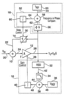
Figure 1 illustrates an embodiment of the present invention. The apparatus is
an
amplifier for continuous high gain, narrowband signal amplification. The
amplifier
includes a first summer 10, an active circuit 12, a feedback circuit 14, a
first controller
16 for adjusting the gain of the active circuit I2 and a second controller 18
for adjusting
the phase of the feedback circuit 14. Each of these elements are described as
follows.
The first summer 10 responds to an input signal 20 and a feedback signal 22.
The
first summer 10 produces an active circuit input signal 24. The active circuit
12, such as
a transistor, diode or other like a variable gain amplifier, responds to the
active circuit
input signal 24 and a gain control signal 26. The active circuit 12 produces
an output
signal 28. The feedback circuit 14 responds to the output signal 28 and a
phase control
signal 30. The feedback circuit 14 produces the feedback signal 22. The first
controller
16 responds to the output signal 28. The first controller 16 produces the gain
control
signal 26. The second controller 18 responds to the output signal 28. The
second
controller 18 producing the phase control signal 30.
In another embodiment of the present invention, illustrated in Figure 2, the
first and
second comptrollers 18 further include the following elements.
The first controller 16 includes a received signal strength indicator 32, a
bandwidth
limit filter 34, a reference voltage source 36, a second summer 38 and a first
loop filter
40. The elements are further described as follows.
The received signal strength indicator 32 responds to the output signal 28.
The
received signal strength indicator 32 produces a RSSI output signal 42. The
bandwidth
limit filter 34 responds to the RSSI output signal 42. The bandwidth limit
filter 34
produces a bandwidth limited signal 44. The reference voltage source 36
produces a
reference voltage signal 46. The second summer 38 responds to the bandwidth
limited
signal 44 and the reference voltage signal 46. The second summer 38 produces
an
amplitude error signal 48. The amplitude error signal 48 is proportional to
the amplitude
CA 02280878 1999-08-06
WO 99/30416 PCT/CA98/01123
-6-
difference between the voltage reference signal and the bandwidth limited
signal 44. The
first loop filter 40, such as an integrator, responds to the amplitude error
signal 48. The
first loop filter 40 produces the gain control signal 26.
The second controller 18 includes a reference frequency source 50 and a phase
locked loop 52. Alternatively, a frequency locked loop may be used instead of
a phase
locked loop. The reference frequency source 50, such as a crystal oscillator,
produces a
reference frequency signal 54. If the phase locked loop 52 is used, the phase
locked loop
52 responds to the reference frequency signal 54 and the phase locked loop 52
produces
the phase control signal 30. Similarly, if a frequency locked loop is used the
frequency
locked loop responds to the reference frequency signal 54 and the frequency
locked loop
produces the phase control signal 30.
If the phase locked loop 52 is used, the phased locked loop includes a
frequency
divider 56, a phase comparator 58 and a second loop filter 60. The frequency
divider 56
responds to the output signal 28. The frequency divider 56 produces a divided
frequency
signal 62. The phase comparator 58 responds to the reference frequency signal
54 and the
divided frequency signal 62. The phase comparator 58 produces a compared
signal 64.
The compared signal 64 is proportional to the frequency difference between the
reference
frequency signal 54 and the divided frequency signal 62. The second loop
filter 60, such
as an integrator, responds to the compared signal 64. The second loop filter
60 produces
the phase control signal 30.
If a frequency locked loop is used, the frequency lock loop includes a
frequency
divider 56, a frequency comparator and a second loop filter 60. The frequency
divider 56
responds to the output signal 28. The frequency divider 56 produces a divided
frequency
signal 62. The frequency comparator responds to the reference frequency signal
54 and
the divided frequency signal 62. The frequency comparator produces a compared
signal
64. The compared signal 64 is proportional to the frequency difference between
the
reference frequency signal 54 and the divided frequency signal 62. The second
loop filter
60, such as an integrator, responds to the compared signal 64. The second loop
filter 60
produces the phase control signal 30.
Figure 3 illustrated yet another embodiment of the present invention. The
amplifier
includes a first summer 10, a variable gain amplifier, a feedback circuit 14,
a first
CA 02280878 1999-08-06
WO 99/30416 PCT/CA98/01123
controller 16 for adjusting the gain of the variable gain amplifier and a
second controller
18 for adjusting the phase of the feedback circuit 14.
The first summer 10 responds to an input signal 20 and a feedback signal 22.
The
first summer 10 produces an active circuit input signal 24. The variable gain
amplifier
responds to the active circuit input signal 24, a course gain control signal
66 and a fine
gain control signal 68. The variable gain amplifier produces an output signal
28.
The feedback circuit 14 responds to the output signal 28, a course phase
control
signal 70 and a fine phase control signal 72. The feedback circuit 14 produces
the
feedback signal 22. The feedback circuit 14 further includes a first amplifier
74, a second
amplifier 76, a third amplifier 78, a fourth amplifier 80, a first course
delay switch 82, a
second course delay switch 83, and a third course delay switch 84 and a fourth
course
delay switch 86.
The first amplifier 74 responds to the output signal 28 and the fine phase
control
signal 72. The first amplifier 74 produces a second amplifier 76 input signal.
The second
amplifier 76 responds to the second amplifier input signal 88 the fine phase
control signal
72. The second amplifier 76 produces a third amplifier input signal 90. The
third
amplifier 78 responds to the third amplifier input signal 90 and the fine
phase control
signal 72. The third amplifier 78 produces a fourth amplifier input signal 92.
The fourth
amplifier 80 responds to the fourth amplifier input signal 92 the fine phase
control signal
72. The fourth amplifier 80 produces the feedback signal 22. The first course
delay
switch 82 responds to a course phase control signal 70. The first course delay
switch 82
controls the first amplifier 74. The second course delay switch 83 responds to
a course
phase control signal 70. The second course delay switch 83 controls the second
amplifier
76. The third course delay switch 84 responds to a course phase control signal
70. The
third course delay switch 84 controls the third amplifier 78. The fourth
course delay
switch 86 responds to the course phase control signal 70. The fourth course
delay switch
86 controls the fourth amplifier 80.
The first controller 16 responds to the output signal 28. The first controller
16
produces the course gain control signal 66 and the fine gain control signal
68. The first
controller 16 further includes a receive signal strength indicator 32, an
analog to digital
converter 94, a course gain control element 96, a band gap reference voltage
source 36,
CA 02280878 1999-08-06
WO 99/30416 PCT/CA98/01123
_g_
a level shifter 98, a fifth operational amplifier 100, a first charge pump 102
and a second
bandwidth limiting filter 104.
The receive signal strength indicator 32 responds to the output signal 28. The
receive signal strength indicator 32 produces a RSSI output signal 42. The
analog to
digital converter 94 responds to the RSSI output signal 42. The analog to
digital
converter 94 produces a digital RSSI output signal 106. The course gain
control element
96 responds to the digital RSSI output signal 106. The course gain control
produces the
course gain control signal 66. The band gap reference voltage source 36
produces a
reference voltage signal 46. The level shifter 98 responds to the reference
voltage signal
46. 'Che level shifter 98 produces a level sifted voltage signal 108. The
fifth operational
amplifier 100 responds to the level shifter signal and the RSSI output signal
42. The fifth
operational amplifier 100 produces a first charge pump input signal 110. The
first charge
pump 102 responds to the first charge pump input signal 110 and a clock signal
112. The
first charge pump 102 produces a first charge pump output signal 114. The
second
bandwidth limiting filter 104 responds to the first charge pump output signal
114. The
second bandwidth limiting filter 104 produces the fme gain control signal 68.
The second controller 18 responds to the output signal 28. The second
controller
18 produces the fine phase control signal 72 and the course phase control
signal 70. The
second controller 18 includes a crystal reference oscillator 50, a frequency
divider 56, a
phase frequency detector 58, a second charge pump 116, a filter 118 and a
counter with
logic 120.
The crystal reference oscillator SO produces the reference frequency signal
54. The
frequency divider 56 responds to the output signal 28. The frequency divider
56 produces
a divided frequency signal 62. The phase frequency detector responds to the
reference
frequency signal 54 and the divided frequency signal 62. The phase frequency
detector
produces a second charge pump input signal 122. The second charge pump 116
responds
to the second charge pump input signal 122 and the clock signal 112. The
second charge
pump 116 produces a second charge pump output signal 124. The filter responds
to the
second charge pump output signal 124. The filter produces the fine phase
control signal
72. The counter with logic responds to the divided frequency signal 62 and the
reference
frequency signal 54. The counter with logic produces the course phase control
signal 70.
CA 02280878 1999-08-06
WO 99/30416 PCT/CA98/01123
_g_
The method of operation is now described. Figure 4 illustrates an
amplification
method for continuous high gain, narrowband signal amplification, the
amplification
method comprising the steps of adjusting the gain 126 of the active circuit 12
and the
phase 128 of the feedback circuit 14 herein the gain and phase adjustments 130
allow
high gain, narrowband amplification of the input signal 24
Figure 5 illustrates the gain adjusting step 126 which includes the following
steps:
Step 132, producing an RSSI signal related to the signal strength of the
output
signal 28;
Step I34, filtering the noise bandwidth of the RSSI signal to produce a
bandwidth limited signal 44;
Step 136, generating a reference voltage signal 46;
Step 138, comparing the reference voltage signal 46 with the bandwidth limited
signal 44 to produce an error signal;
Step 140, integrating the error signal;
Step 142, producing an amplitude control signal based upon the integrated
value of the error signal; and
Step 144, adjusting the gain of the active circuit 12 based upon the value of
the
control signal.
Figure 6 illustrates the phase adjusting step 128 which includes the following
steps:
Step 146, producing a divided frequency signal 62 by dividing the output
signal
28 to a lower frequency;
Step 148, counting the divided frequency signal 62 over a predetermined
interval of time;
Step 150, comparing the result of the count with the expected number of counts
of the reference over the same period of time;
Step 152, limiting the bandwidth of the comparison; and
Step 154, adjusting the delay of the feedback circuit 14 based upon the
results
of the band-limited comparison.
Finally, advantages of the various embodiments of the invention are now
described.
A description of a number of alternative implementations are also included.
Firstly, the
control loops use the thermal noise in the amplifier to maintain the amplifier
in a high
CA 02280878 1999-08-06
WO 99/30416 PCT/CA98/01123
-10-
gain, narrowband amplification state. There is a feedback loop in the
amplifier, hence the
thermal noise power grows from startup in a manner analogous to the growth of
the
thermal noise power in an oscillator. The present invention however, has the
advantage
that the control loops use the thermal noise to maintain the amplifier in a
state close to,
but not equal to, oscillation. The result is high gain, narrowband
amplification.
Furthermore the variable gain amplifier, may have both fine gain adjust and a
crude
or discrete gain adjust. The fine gain adjust is such that it has a very
limited gain adjust
over a large control voltage. This is useful to allow the amplifier to reach
the tight levels
of gain controls. The discrete gain adjust is used to place the amplifier at a
gain within
the control range of the fine gain adjust. The discrete gain adjusts are noise
immune as
they are of a switched nature and do not rely on a low noise analog control.
The need for
the discrete gain adjust and the number of discrete levels required depends
upon the
precision and the Q levels to be achieved and on the precision of the
integrated circuit
processes being used.
The filter to limit the bandwidth of the receive signal strength indicator
(RSSI)
output may limit noise and upper order signal harmonics generated by the RSSI.
Optionally, an advantage is to measure the output of the amplifier in discrete
steps
using the analog to digital converter 94 therefore allowing the gain to be
adjusted in
discrete steps to within the fine adjust range where the integrator takes
over.
The frequency of the signal being generated or filtered is controlled by the
delay
in the feedback circuit 14. It is difficult In an integrated circuit to
accurately achieve this
delay without some form of feedback. The preferred embodiment of this
invention is to
limit the range of delays using some physical means, which limits the range of
possible
amplification frequencies. The practical limits should take into account the
tolerances
achievable on a given integrated circuit process.
Depending upon the application, the fine frequency adjust used in the
invention
may be achieved in a number of different forms. If a low phase noise signal
source is
desired then a crystal oscillator reference should be used with a phase locked
loop 52
(PLL). This type of circuitry is readily achievable in integrated circuit form
with only
the crystal itself and portions of the PLL low pass loop filter required
external to the
integrated circuit. In the simplest form the reference may be chosen as a
fixed integer
CA 02280878 1999-08-06
WO 99/30416 PCT/CA98/01123
-11 -
sub-multiple of the desired output frequency. In a more advanced variation of
the
invention the reference may be operated in a variable PLL which can achieve
many
sub-multiple division ratios, including rational numbers such as might be
achieved with
a fractional-N synthesizer based PLL for example.
If the in-close phase noise of the amplifier is not a requirement for the
application,
as may be the case say for some less demanding applications, then the
frequency control
loop may be simplified to a simple frequency locked loop (FLL). This type of
loop
counts the output frequency over a long period of time, and compares the
result with a
similar count of the reference frequency over the same period of time. The
comparison
is used in its simplest form to decide to adjust the delay of the feedback
circuit 14 up or
down, to achieve the correct output frequency. The tolerance of the output
frequency will
be approximately the accuracy of the crystal in parts-per-million, or the
reciprocal of the
count interval, which ever is greater. Typically a low noise fine frequency
control loop
can be built with a charge pump on an integrated circuit which pumps up or
down to
adjust the frequency. The optional fine phase adjust can be achieved in a
number of
ways. One method is to use a voltage variable capacitance, such as a bipolar
transistor
junction in back bias, as the delay adjust element.
Similar to the amplitude control loop the delay can be implemented with fine
and
crude adjustments, with the crude steps adjusted by discrete means and the
fine adjust
controlled by means of a large voltage to control a fine delay adjust. This is
the most
noise immune approach. Again requirement for the crude adjust, and the number
of
levels of crude adjust will be determined by the precision of the application
and the
tolerances of the integrated circuit process used.
All of the above adjusts may meed to be done in crude discrete steps and in
fine
vernier steps depending upon the application. This does not change the
generality of the
invention.
The feedback filter may also be realized as any form of bandpass filter such
as an
LC filter. Furthermore, the amplifier may be redrawn as a tuned amplifier.
Moreover,
throughout the description altering the delay of the feedback circuit 14 is
functionally
equivalent to altering the phase of the feedback circuit 14.
CA 02280878 1999-08-06
WO 99/30416 PCT/CA98/01123
-12-
Numerous modifications, variations and adaptations may be made to the
particular
embodiments of the invention described above without departing from the scope
of the
invention, which is defined in the claims.