Note: Descriptions are shown in the official language in which they were submitted.
CA 02281039 2001-06-14
NOVEL OPTICAL SCHEME FOR HOLOGRAPHIC IMAGING OF COMPLEX
DIFFRACTIVE ELEMENTS IN MATERIALS
FIELD OF THE INVENTION
This invention relates generally to a method and system for inducing a
refractive index change in a light transmissive material, such as glass, or
absorbing material such as metal, but not limited thereto.
BACKGROUND OF THE INVENTION
The manufacture of many photonics devices are based on the ability to
create permanent photorefractive changes in transparent materials. For
example, the development of Bragg grating reflectors within planar or linear
waveguides such as single mode optical fibres is well known and has been
described in various United States patents. For example, one type of a Bragg
filter, is incorporated or embedded in the core of an optical fiber by a
method
disclosed, in United States patent number 4,807,850. As is discussed in this
patent, permanent periodic gratings of this kind can be provided or impressed
in
the core of an optical fibre by exposing the core through the cladding to the
interference pattern of two coherent beams of ultraviolet light that are
directed
against the optical fibre symmetrically to a plane normal to the fiber axis.
This
results in a situation where the material of the fiber core has permanent
periodic
variations in its refractive index impressed therein by the action of the
interfering
ultraviolet light beams thereon, with the individual grating elements (i.e.
the
CA 02281039 2001-06-14
periodically repetitive regions of the core exhibiting the same refractive
index
behavior) being oriented normal to the fiber axis so as to constitute the
Bragg
grating.
Other more popular methods of writing Bragg gratings in optical fibre are
taught by Anderson in U.S. Patent No. 5,327,515, and by Hill in U.S. Patent
No.
5,367,588. Both Anderson and Hill utilize a phase mask or optical phase
grating.
An interference pattern is generated by impinging a single light beam on the
phase mask. The optical waveguide to be processed is exposed to the
interference pattern, leading to the formation of a Bragg grating in the
waveguide. In all of these prior art examples, an optical fibre having a Ge
doped
photosensitive core is irradiated with UV light of a predetermined intensity
and
for a predetermined duration sufficient to obtain a substantially permanent
grating therein.
Although these prior art gratings provide a useful function, it would be
advantageous to be able to write a grating in an un-doped light transmissive
substrate or waveguide such as a typical telecommunications optical fibre, or
on
a slab waveguide device.
Aside from the drawback of having to provide specialty optical fibre by
way of doping the core of an optical fibre so that the core becomes
photosensitive to UV light, or additionally exposing such doped fibres to H2
or
Deuterium gas at high temperatures for a substantial duration and under
substantially high pressures so that its core becomes more photosensitive,
2
CA 02281039 2004-11-05
optical fibre having a grating impressed therein, in the traditional manner
has be
joined to the telecommunications fibre to which it is to be coupled with. Of
course, H2 loading and splicing fibre adds the cost and to the associated
signal
loss by virtue of having a coupling or splice joint between two optical
fibres,
Refractive index changes written in standard UV-photosensitive optical
materials such as Ge-silicate glasses are normally limited to a refractive
index
difference ~n <10-3. Recently, research has been directed toward elucidating
the
mechanism for photorefractive index changes in glasses upon exposure to UV
light, and progress has been made toward developing materials with enhanced
photosensitivity, e.g, hydrogen loaded specially- doped silicate glasses for
waveguiding applications, or photorefractive gels for bulk diffractive
elements.
However each of these materials suffer in one way or another from inferior
optical or mechanical properties compared with normal optical glasses. Often a
curing process is required following UV exposure, which can cause shrinkage
and distortion of the optically written pattern. Photorefractive gels, in
particular,
are limited in their application due to the non-permanent nature of the index
change, with decays on a timescale of a few years.
An alternative mechanism which employs high-intensity ultra-fast pulses
for creating permanent photorefractive changes in glasses has recently been
explored by several groups of researchers. Such disclosure can be found in a
paper by K.M. Davis, et al. in Opt. Lett. 21, 1729 (1996) and in a paper by
E.N.
Giezer et al in Opt. Lett. 21, 2023, (1 996). Giezer et al. reported
refractive index
3
CA 02281039 2001-06-14
changes of On ~ 0.1 written in fused silica using tightly focused pulses with
peak
intensities ~ 10 '3 W/cm2 . The physical process that gives rise to this
refractive
index change appears to be due to the creation of free electrons through multi-
photon ionization of bound charges, followed by avalanche ionization and
localized dielectric breakdown as these fee electrons are accelerated by the
intense laser field. Phenomenologically, this leads to a localized melting and
compaction of material, and a concurrent increase in the index of refraction.
Owing to the extremely high intensities of light required to activate this
photo-
refractive mechanism, work performed in this field has used pulses that are
tightly focused to near-diffraction limited spots. While this allows high-
resolution
spatial localization of the refractive index change to a volume on the order
of 1 -
0 Nm3 , it also requires that the laser focus be scanned point-by-point
throughout three dimensions to build up a complete hologrammatic pattern in
the
material. This is a great disadvantage for writing diffractive structures that
have
extended dimensions, since mechanical precision of A100 must be sustained
across length scales up to centimeters. Over time-scales of minutes, slight
drifts
in ambient temperature can lead to thermal expansions or contractions that
often
limit the accuracy of the fabrication process. Since raster scanning is an
inherently slow procedure, this technique is not well-suited toward writing
large
diffractive structures.
Providing a hybrid technique of utilizing standard phase masking
techniques in combination with using ultra short high power femto-second
pulses
4
CA 02281039 2001-06-14
is problematic, since close coupling a phase mask to create an interference
pattern in a sample is not feasible; the mask will experience optical damage
due
to the high peak intensity of light required at the sample position.
Hence, in accordance with this invention, the mask must be located
remotely and the diffracted light accurately imaged onto a small spot at the
sample.
Since a phase mask introduces high angular dispersion in the diffracted
beams, due to the broad spectral content of ultra-short pulses, simply
redirecting
each individual diffracted beam so that they overlap in the sample,
unfortunately
results in a greatly reduced peak intensity as the spectral content of the
pulse is
distributed over a relatively large area.
SUMMARY OF THE INVENTION
Thus, in accordance with a preferred embodiment of this invention, an
imaging system is provided that overlaps replicas of the short pulse without
significant spatial or spectral aberrations, and without any element
experiencing
peak intensifies within two orders of magnitude of those at the sample.
It is an object of this invention to overcome many of the aforementioned
limitations within the prior art systems of inducing a refractive index change
in a
light transmissive material.
It is an object of this invention to provide a system and method for writing
gratings and patterns distinguishable by way of having a plurality of
refractive
5
CA 02281039 2001-06-14
index changes in un-doped optical glass.
It is yet a further object of the invention, to provide a system and method
for inducing a refractive index change region of a piece of light transmissive
material that is not doped to become highly photosensitive.
In accordance with an aspect of the invention, there is provided, an
optical system for writing a spatial modulated index pattern in a material
that is
at least partially light transmissive or partially absorbing, comprising:
an ultrafast light source for generating a pulse of laser light;
a diffractive optic element having predetermined characteristics, said
element being disposed to receive the pulse of laser light;
an imaging and concentrating system disposed to receive at least some
divergent light beams from the diffractive optic element and for concentrating
and imaging received light beams at the material, the imaging and
concentrating
system including:
a) a curved mirror disposed to receive said at least some of the divergent
light beams from the diffractive optic element and to reflect the received
light
beams in a substantially wavelength independent manner, and
b) a concentrating/focusing element for focusing and concentrating light
beams reflected from the curved mirror onto the at least partially light
transmissive or partially absorbing material to effect a permanent refractive
index change within the material that corresponds to the spatial modulated
index
pattern, said curved mirror and said concentrating/focusing element being
6
CA 02281039 2001-06-14
positioned relative to each other and to said diffractive optic element so as
to
affect each of the light beams focused and concentrated onto the at least
partially light transmissive or partially absorbing material in substantially
the
same way in order to preserve a stable phase relationship therebetween.
In this aspect of the invention the pulse may have a duration of less than
picoseconds and multiple pulses may be provided.
In accordance with an aspect of the invention there is provided a method
for writing a spatial modulated index pattern in a material that is at least
partially
transmissive or partially absorbing comprising the steps of:
10 a) providing a pulse of laser light from an ultrafast laser;
b) providing a diffractive optic element having predetermined
characteristics and directing the short pulse of laser light to be incident
upon the
diffractive optic element;
c) disposing an imaging and concentrating system to receive multiple light
beams diffracted from the diffractive optic element and for concentrating the
light
beams received at the material, step (c) including the sub-steps of:
i) said imaging and concentrating system including a curved mirror for
reflecting the multiple light beams from the diffractive optic element in a
substantially wavelength independent manner; and
ii) said imaging and concentrating system including means for receiving
the light beams reflected from the curved mirror and concentrating and
focusing
said light beams received from the curved mirror onto the light transmissive
7
CA 02281039 2001-06-14
material to effect a permanent refractive index change within the material
that
corresponds to the spatial modulated light pattern, said curved mirror and
said
means for receiving and concentrating are positioned relative to each other so
as to affect each of the multiple light beams in substantially the same way
for
preserving a stable phase relationship between said multiple light beams at
said
material.
In this aspect of the method a plurality of pulses of light may be provided.
In accordance with another aspect of the invention there is provided a
method of effecting a refractive index change in a sample that is at least
partially transmissive or partially absorbing comprising the steps of:
providing a short pulse laser beam having a low power per unit area to a
diffractive optical element so as to irradiate the diffractive optical
element;
collecting light from the diffractive optical element while preserving an
image relating to characteristics of the diffractive optical element encoded
within
the light collected; and
directing the light collected in wavelength independent manner to the
sample while preserving the image of the diffractive optical element encoded
within the light collected and demagnifying the image within the light
collected so
as to increase its power per unit area when directed to the sample to be
permanently impressed therein, wherein the steps of collecting the light from
the
diffractive optical element and directing the light collected in wavelength
independent manner includes preserving a stable phase relationship between
8
CA 02281039 2001-06-14
components of the light collected.
In accordance with another aspect of the invention there is provided an
optical system for writing a refractive index pattern in a sample that is at
least
partially light transmissive or partially light absorbing comprising:
means for providing a short pulse laser beam having a low power per unit
area;
a diffractive optical element disposed to receive the short pulse laser
beam;
means for collecting multiple light beams transmitted through or reflected
from the diffractive optical element and for preserving an image relating to
characteristics of the diffractive optical element encoded within the multiple
light
beams collected, and for directing the multiple light beams collected in
wavelength independent manner while preserving the image of the diffractive
optic element encoded within the light beams collected for demagnifying the
image within the multiple light beams collected so as to increase the power
per
unit area when the multiple light beams collected are directed to the sample
to
be permanently impressed therein, and said means for collecting multiple light
beams transmitted through or reflected from the diffractive optical element
and
for directing the multiple light beams collected includes optical elements
which
are positioned relative to each other and to said diffractive optic element so
as to
affect each of the multiple light beams collected in substantially the same
way for
preserving a stable phase relationship therebetween.
9
CA 02281039 2001-06-14
In accordance with another aspect of the invention a method is provided
for producing multiple light beams from an ultrafast laser with
interferometric
stability between the multiple beams, comprising the steps of:
a) providing a pulse of laser light from an ultrafast laser;
b) providing a diffractive optic element having predetermined
characteristics and directing the pulse of laser light to be incident upon the
diffractive optic element; and
c) capturing and reflecting multiple light beams diffracted from the
diffractive optic element in a substantially wavelength independent manner,
said
multiple light beams being captured and reflected using optical elements which
are positioned relative to each other and to said diffractive optic element so
as to
affect each of the multiple light beams in substantially the same way for
preserving a stable phase relationship therebetween.
In this aspect of the invention a plurality of pulses may be provided.
This invention provides a system and method of mapping an image from a
wavelength dispersive element via a wavelength independent
concentrating/focusing system to a light transmissive medium so that a feature
of
the wavelength dispersive element can be permanently recorded within the light
transmissive medium. The system and method rely on the use of a high power
short pulse of laser light at the wavelength dispersive element.
This invention further provides a system and method of mapping an
image from a wavelength dispersive element via a wavelength independent
CA 02281039 2001-06-14
concentrating/focusing system to a light transmissive or absorbing medium so
that a feature of the wavelength dispersive element can be permanently
recorded within a light transmissive or absorbing medium by providing a
relatively short pulse of laser light, having a substantially broad beam
diameter
with a low power per unit area so as to prevent damage to the wavelength
dispersive element, wherein the wavelength independent concentrating focusing
system transforms said beam into overlapping beams along image plane where
the intensity per unit area of regions along the image plane is substantially
greater than the intensity per unit area of the beam at the wavelength
dispersive
element.
In summary, this invention provides a short pulse laser beam having a low
power per unit area to a diffractive optical element. The image produced by
irradiating the diffractive optical element with the short pulse laser beam is
collected by a wavelength independent element and imaged and demagnified so
as to increase its power per unit area when directed to the light transmissive
or
light absorbing sample to be permanently recorded therein,
BRIEF DESCRIPTION OF THE DRAWINGS
Exemplary embodiments of the invention will now be described in
conjunction with the drawings in which:
Fig. 1 is a pictorial view of an optical circuit including a spherical mirror
and a cylindrical lens for writing images in an optical medium such as un-
doped
11
CA 02281039 2004-11-05
glass using femtosecond optical pulses;
Fig. 2 is a pictorial view of an alternative embodiment of the invention
wherein the spherical mirror and lens of Fig. 1 are replaced with finro
parabolic
mirrors;
Figs. 3a is a diagram illustrating a pulse crossing geometry using a
conventional beam splitter to generate two pulse replicas;
Fig. 3b illustrates the generation of pulse replicas with tilted wavefronts
using a diffractive optic element;
Fig. 4a is a diagram of a prior art optical 4f imaging system; and,
Fig. 4b is a diagram illustrating how geometric aberration within the
system shown in Fig. 4a can result in wavelength dependent focusing.
DETAILED DESCRIPTION OF THE INVENTION
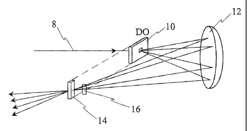
Turning now to Fig. 1, an optical circuit representing an imaging system in
accordance with the invention is shown. The method of the invention will
become
apparent by way of explanation of the operation of the optical circuit.
At the upper left corner of Fig 1, line 8 representing a pulse of laser light
having duration of 10 -'4 to 1 0 -" seconds is shown impinging upon a
diffractive
element 10. The diffractive element (DO) 10 is preferably in the form of a
phase
mask, for example having a predetermined surface relief pattern that will
produce
a wave front having predetermined characteristics at its output end face in
response to an input pulse of laser light. The DO 10 is designed to produce an
12
CA 02281039 2001-06-14
image at its output end face and that image is to be impressed in a light
transmissive element, preferably in the form of a piece of un- doped glass 14.
Alternatively, instead of the phase mask 10 an amplitude mask could be
utilized,
however is less preferred.
Yet still, alternatively a reflective diffractive optic element can be used
instead of a transmissive element. However, such a reflective element should
be
coated to achieve high reflectivity of the laser power; in practice, such a
coating
tends to smear out the surface relief pattern on the diffractive element,
reducing
the diffraction efficiency and limiting the throughput to the light
transmissive
material14.
In Fig. 1, a 300 mm radius f/1 spherical mirror 12 is disposed adjacent to
the DO 10 such that the DO 10 is at the radius of curvature of the mirror 12.
In
operation, as the one-shot short pulse of light incident upon the DO
propagates
therethrough, a wave front having characteristics of the DO encoded therein,
exits the DO 10 and is highly divergent. The mirror 12, provides a means of
receiving the highly divergent light and reflects the light in a wavelength
independent manner to the un-doped glass 14. A rod lens 16 is disposed
between the mirror 12 and the un-doped sample of glass and provides a means
of concentrating the light within the image by demagnifying the image. More
simply stated, a substantially large beam of light having finite amount of
energy
in the form of a short femtosecond pulse is utilized to image the phase mask
at
its output end face. This larger image collected from about the phase mask is
13
CA 02281039 2004-11-05
preserved and relayed in a wavelength independent manner to the lens 16,
which performs a scaling function and reproduces a more intense replica of the
image than was present at the output end face of the phase mask 10 upon the
glass 14.
The circuit of Fig. 1 provides a system and method for holographic
fabrication of one dimensional periodic structures within a transparent
material
by the application of one or more single-shot femtosecond pulses of light.
Thus,
a desired pattern dependent upon the characteristics of the DO 10, is encoded
upon exposure to a single laser pulse.
There is a consideration related to generating large-dimension
interference patterns with ultra-fast pulses that is not relevant for
generating
similar patterns with long pulse sources. To create an interference pattern,
two
phase-coherent replicas 32 and 34 of the laser pulse 30 provided by pulse 30
being incident on beamsplitter 28 must be overlapped in the sample plane 36 as
shown being done by a spherical mirror 38 with their wave fronts tilted with
respect to one another as shown in Fig. 3a. At any point in time, an ultra-
fast
pulse 30 can be viewed as a spatially localized wave packet of light, whose
transverse dimensions are those of the laser beam and whose longitudinal
dimension is cat, where c is the speed of light and ~t the temporal pulse
width. If
two replicas 32 and 34 of the short pulse 30 are crossed at an angle, the
region
40 in which they are spatially overlapped will be limited to a transverse
dimension of -2c~t/tan(6), where 8 is the crossing angle between beams. For
14
CA 02281039 2004-11-05
devices operating at optical or near IR wavelengths, grating periods on the
order
of n~1 pm are of greatest interest, which implies A ~ 1 radian for 800 nm
excitation wavelengths. The maximum spatial dimension that can be written in
this case will then be limited to ~ 40 pm. Generally, device lengths will not
be
able to exceed dimensions of a few tens of grating periods along the direction
of
the grating wave vector due to this problem. With reference to region 42 shown
in Fig. 3b, the arrangement of Fig. 3b is absent the geometric smearing of the
pulse overlap region 40 that is present in Fig. 3a. The ovals shown represent
a
view at an instant in time of the spatial pulse envelope, and the parallel
lines
inside the ovals represent the wave fronts.
Despite the limitations of the phase masking technique, the method and
circuit in accordance with this invention does eliminate the short-pulse
overlap
problem. As an illustrative example of how this works, consider the simple
situation depicted in Fig. 3b, in which an incident short pulse 60 is
diffracted into
two orders 62 and 64 by diffractive optic 10. Since the pulse envelope is not
changed upon diffraction, immediately following the phase mask 10 there is
still
perfect spatial overlap between the two pulse replicas 62 and 64. Thus, the
use
of phase mask 10 extends the overlap regions for single-shot writing of
different
structures using ultra fast pulses to dimensions on the order of the input
beam
diameter (~1 mm). In addition, the spatial period of the interference pattern
between different diffractive structures using ultra fast pulses to dimensions
on
the order of the input beam diameter (~ 1 mm). In addition, the spatial period
of
CA 02281039 2004-11-05
the interference pattern between different diffractive orders will be
independent
of the source wavelength, since each spectral component will be diffracted by
the mask 10 into a slightly different direction.
The optical system and method of Fig. 1 preserves the desired features of
the phase mask approach while allowing high intensifies at the sample, while
correcting the detrimental effects of angular dispersion arising from the
mask.
For simplicity, only two separate beams are shown following the mask, although
this system can in general image any one-dimensional mask pattern or even
more complex patterns onto the sample. An ultra-fast laser pulse in a 1 mm
diameter collimated beam is incident on the phase mask, which generates pulse
replicas with tilted wave packets. The mirror 12 having the DO 10 located at
its
centre of curvature retroreflects the diffracted light collected from the DO
10,
regardless of the diffraction angle or the optical wavelength. The mirror 12
is
tilted slightly off-axis to separate the incoming beams from the outgoing
beams,
which are directed towards the sample. At the sample 14 position, the various
diffractive orders overlap and produce an interference pattern-that is the
inverted
image of the intensity distribution following the phase mask. At high enough
intensifies, a hologrammatic replica of the phase mask will be created in the
sample via the photorefractive mechanism discussed above. To achieve these
intensifies, the input beams are concentrated in one spatial dimension by a 10
mm focal length cylindrical lens, resulting in approximately 100 x greater
intensity
at the sample than at the input mask. While tight focusing unavoidably
distorts
16
CA 02281039 2004-11-05
the image in the focus dimension, this is of no consequence for writing one-
dimensional periodic structures.
This imaging system bears some analogy to a typical "4f"imaging system
shown in Figs. 4a and 4b, used in Fourier optics for image processing and
pulse
shaping. Particularly, Fig. 4a is a diagram of a prior art optical 4f imaging
system
which includes two 4f lenses 70 equally spaced on either side of a plane 72
for
focusing images produced by a beam splitter 74 at an object plane 76 onto an
image plane 78. Fig. 4b is a diagram illustrating how geometric aberration
within
the system shown in Fig. 4a can result in wavelength dependent focusing.
Like the 4f system, the arrangement used in this instance has a delta-
function impulse response- function; hence the image at the input plane is
perfectly reconstructed at the sample. An immediate consequence of this
property is that the arrangement shown in Fig. 1 corrects for angular
dispersion
of the pulse spectrum that arises due to diffraction from the phase mask 10.
Advantageously, the optical system in accordance with this invention
affords a high degree of interferometric stability between the various
diffracted
beams which is required to preserve a constant phase relationship between the
beams at the sample, so that the interference pattern on the substrate does
not
shift appreciably over the time scale of exposure. The origin of this
stability lies in
the fact that all of the beams interact with the same set of optical elements,
so
that small mechanical fluctuations of any of the elements in the beam paths
affect each beam in approximately the same manner, and thus do not
17
CA 02281039 2004-11-05
appreciably perturb their relative optical path lengths.
Fig. 2 illustrates an alternative and preferred embodiment of the invention
which provides a simple manner of scaling the image that is to be imprinted in
the un-doped glass sample. Similar to the embodiment of Fig. 1, an ultra short
pulse of light having a duration of tens of femtoseconds is provided and is
launched into the DO 10. A first parabolic mirror 22 having a focal length f1
is
disposed to receive the diffracted light that has transmitted through is
diverging
from the DO 10. Of course the parabolic mirror 22 is sized to capture and
reflect
most of the light energy of the incident short pulse provided to and emanating
from the DO 10. A second parabolic mirror 24 having a focal length f2 is
disposed to receive substantially all of the reflected light containing an
image
characteristic of the phase mask encoded in the light, and to concentrate the
image in a reduced replica, having an average greater power per unit area,
sufficient to cause a refractive index change within the glass substrate that
corresponds to the characteristic of the phase mask DO 10. In this embodiment,
the two parabolic mirrors 22 and 24 provide essentially the same functionality
provided by the curved mirror 12 and lens 16 in Fig. 1 in the instant
embodiment,
the parabolic mirrors are spaced by a distance (f1 + f2); the magnification is
f2/f1, and hence the demagnification is f1/f2. The peak intensity at the
workpiece
or glass substrate is (f1/f2)2 times larger than at the DO 10. This embodiment
is
suitable for 2D patterns. The embodiment shows focal length f2 being shorter
than focal length f1.
18
CA 02281039 2004-11-05
In Fig. 2 the two parabolic mirrors 22 and 24 serve as the optical imaging
and concentration means, whereas in Fig. 1, the spherical mirror 12 and
cylindrical lens 16 provide this function.
There are numerous applications of the holographic system in accordance
with this invention. Amplified Ti: sapphire laser systems are capable of
emitting
100 fs pulses with 1 mJ of energy at kilohertz repetition rates. This high
pulse
repetition frequency lends itself to scanning the location of the interference
pattern on the sample to produce larger structures. By taking advantage of
existing precision optical alignment methods used in fabricating fibre Bragg
gratings, photo-written gratings can be laid sequentially end-to- end with
excellent control over the relative grating phase, resulting in periodic
structures
with dimensions far greater than those which can be fabricated on a single
shot
basis. In addition structures with large transverse dimensions can easily be
made as well simply be scanning the beam in the dimension perpendicular to the
grating wave vector. Since the high-intensity photorefractive mechanism
appears
to be present in virtually all common optical materials, strongly modulated
structures can be made in un-doped glasses which are not UV-photosensitive.
Finally, the 800 nm excitation wavelength is only very weakly absorbed in most
materials, which will naturally, enable the formation of the deep structures,
limited only by nonlinear pulse breakup effects that will eventually reduce
the
peak intensity after ~ millimeter propagation distances. Thus, the method
presented in accordance with this invention should enable fabrication of large
19
CA 02281039 2004-11-05
volume (> 1 mm3), bulk diffractive elements in virtually any optical material.
Numerous other embodiments may be envisaged, without departing from
the spirit and scope of the invention. For example, there are also numerous
applications in laser based medical treatments to which this invention can
apply.
For example, one can contemplate writing structures in the cornea or achieve
very precise beam alignments to execute an operation.
With conventional technology for writing structures in light transmissive
materials, it is very difficult to write similar patterns in light absorbing
materials.
Although exemplary embodiments of the invention have been described
heretofore with respect to effecting a pattern in light transmissive
materials, it is
not exclusive to transmissive materials and encompasses writing structures in
a
host of other materials such as absorbing to strongly absorbing materials, for
example writing complex structures in metal surfaces for profiling, where one
desires a complex pattern with high spatial fidelity in a material processing
step
that requires high intensity pulses as are provided for by this invention.
Furthermore, the additional step of passing the light diffracted from the
diffractive optic element through a spatial filter to filter predetermined
orders of
light may be included. For example, zero order nulling of the zeroth order
light
emanating from the filter may be desired.
20