Note: Descriptions are shown in the official language in which they were submitted.
CA 02281044 1999-08-27
Doc. No. 10-126 CA Patent
Optical Multiplexor/Demultiplexor
Field the Invention
This invention relates to a diffraction grating that may be used as a
spectrometer,
a demultiplexor or a multiplexor.
Background Art
l0 In wavelength division multiplexed optical communication systems, many
different optical wavelength carriers provide independent communication
channels in a
single optical fiber. Future computation and communication systems place ever-
increasing demands upon communication link bandwidth. It is generally known
that
optical fibers offer much higher bandwidth than conventional coaxial
communications;
15 furthermore a single optical channel in a fiber waveguide uses a
microscopically small
fraction of the available bandwidth of the fiber (typically a few GHz out of
several tens of
THz). By transmitting several channels at different optical wavelengths into
an fiber (i.e.,
wavelength division multiplexing, or WDM), this bandwidth may be more
efficiently
utilized.
There have been many attempts to develop a compact, high resolution waveguide
demultiplexor or spectrometer for application in areas such as spectroscopy,
optical
networks and optical links and more particularly optical communication
systems. Such a
demultiplexor can be extremely critical in wavelength division multiplexing
(WDM)
links. In these links or networks, each channel is assigned a distinct and
unique
wavelength for data transmission. Thus, the optical fiber that connects
channels in a
WDM network carries many discrete wavelength channels and a particular
wavelength is
selected before the data is received. The data reception can be achieved by
combining a
wavelength demultiplexor, photodetectors and electronic selection circuitries.
In WDM
links, many wavelengths are multiplexed and transmitted through a single
optical fiber to
increase the capacity of the fiber. The receiver must demultiplex the many
wavelengths
CA 02281044 1999-08-27
Doc. No. 10-126 CA Patent
and select the proper channel for reception. In these applications, the
requirements on the
wavelength demultiplexor are currently: an optical bandwidth - 0.4 nm, a
wavelength
resolution of - 0.8 nm, polarization insensitivity, compactness, low loss, low
crosstalk,
and a low manufacturing cost.
At present, there are many known methods of selecting particular wavelengths,
however, none are ideal for the applications outlined above. Such methods rely
either on
bulk optics or waveguide structures where the frequency selective element is
either an
interference grating or a Fabry-Perot (F-P) cavity. Diffraction gratings have
been known
l0 for many years and produce a high resolution spectrum where the wavelength
is a
function of the diffracted angle. Thus a single grating can demultiplex many
wavelengths.
Bulk optics such as these diffraction gratings have offered a reasonably
reliable solution
but have not offered the required bandwidth often providing demultiplexing
with
channels being too narrow for required WDM applications. The limitation of
these
gratings to provide wide band demultiplexed channels has been the large
interspacing
between cores of input or output (input/output) waveguides. For example,
typically arrays
of optical fibres each having an outer diameter of 125pm and a core diameter
of l Opm
are disposed adjacent one another in the form of a ribbon of fibres as input
or output
optical fibres. Such an array is disposed adjacent a diffraction grating and
serves as a
group of receiving fibres in a demultiplexor configuration. A lens is
generally disposed
between the array of optical fibres and the diffraction grating for Tensing
and focusing
diffracted wavelengths of light onto particular optical fibres such that each
optical fibre in
the array is disposed to receive a different channel or wavelength of light
that has been
core diameter
demultiplexed by the diffraction grating. Since the of the array of
core separation
bandwidth
optical waveguides in such a demultiplexor is proportional to the
channel separation
providing an array of optical waveguides having a closely spaced cores, i.e.
little
separation and a standard l Op,m core size will ensure that the bandwidth will
be
reasonably large. This is a result of the core separation being inversely
proportional to the
2
CA 02281044 1999-08-27
Doc. No. 10-126 CA Patent
bandwidth. Hence, if core diameter and bandwidth are fixed lessening the core
separation
will increase the bandwidth.
Techniques for multiplexing and demultiplexing between a single optical fiber
comprising the multiplexed channel and plural optical fibers comprising the
plural
demultiplexed channels are described in various U.S. patents. For example,
multiplexing/demultiplexing with birefringent elements is disclosed in U.S.
Pat. Nos.
4,744,075 and 4,745,991. Multiplexing/demultiplexing using optical bandpass
filters
(such as a resonant cavity) is disclosed in U.S. Pat. Nos. 4,707,064 and
5,111,519.
Multiplexing/demultiplexing with interference filters is disclosed in U.S.
Pat. Nos.
4,474,424 and 4,630,255 and 4,735,478. Multiplexing/demultiplexing
(multiplexing or
demultiplexing) using a prism is disclosed in U.S. Pat. No. 4,335,933. U.S.
Pat. No.
4,740,951 teaches a complex sequence of cascaded gratings to demultiplex
plural optical
signals. U.S. Pat. Nos. 4,756,587 and 4,989,937 and 4,690,489 disclose optical
coupling
between adjacent waveguides to achieve a demultiplexing function. A similar
technique
is disclosed in U.S. Pat. No. 4,900,118. Unfortunately, the foregoing
techniques are
limited by their discrete components to a small number of wavelengths in the
multiplexed
channel.
2o One way of overcoming such a limitation is to employ diffraction gratings
to perform
the multiplexing and demultiplexing functions as is shown by U.S. Pat. Nos.
4,111,524
and 4,993,796. Heretofore, close spacing of the multiplexed and demultiplexed
channels
makes fabrication awkward and increases the likelihood of cross-talk. One way
of
overcoming this latter difficulty is to employ a curved diffraction grating
which reflects
the incoming signal at right angles. These curved gratings are known as
Echelle gratings.
Various such gratings are described in US Pat. No. 5,206,920 in the name of
Cremer et
al; Appl Phys Lett Vol. 58 No. 18 May 1991 p1949 Soole et al; Phot. Tech.
Letts. Vol. 4
No.l 1992 p 108 Cremer et al.; Appl Phys Lett Vol. 61 No.23 Dec. 1992 p 2750
Soole et
al.; Elec. Letts. March 1994 vol. 30 No. 6 p 512 Poguntke et al.; Elec. Letts.
Sept. 1994
3o Vol. 30 no.l9 p 1625 Cremer et al; and, Phot. Tech. Letts. Vol. 6 no. 9 p
1109 Clemens
3
CA 02281044 1999-08-27
Doc. No. 10-126 CA Patent
et al. The manufacture of Echelle gratings is dependent upon etching of high
quality
facets with well controlled side-wall angle and low rounding.
Limitations in fabrication of these gratings have been overcome in a technique
in
which a diffraction grating is combined with a lens, as disclosed in U.S. Pat.
Nos.
4,777,663; 4,839,884; 4,367,040 and 4,739,501. The advantage of the lens and
grating
combination is that the plural optical fibers of the demultiplexed channels
may interface
directly with the single optical fiber of the multiplexed channel through the
grating and
lens combination.
to
Thus, there is a need for compact, manufacturable wavelength division
multiplexing (WDM) device for telecommunications purposes and for other
applications
such as compact spectrometers which provide wide band channels.
It is therefore an object of this invention to provide a diffraction grating
that is
relatively inexpensive to manufacture and compact.
It is an object of this invention to provide a multiplexor or demultiplexor
capable
of demultiplexing relatively closely spaced channels each having a relatively
wide
2o bandwidth.
It is a further object of the invention to provide a multiplexor or
demultiplexor
having in input/output fibre having a different mode field diameter than that
of the
waveguides of a concentrator chip for receiving/transmitting signals, allowing
tuning of
the device during manufacture.
Summary of the Invention
In accordance with the invention, an optical demultiplexor is provided
comprising:
3o a wavelength dispersive optical element for separating a beam into
demultiplexed beams
of light;
4
CA 02281044 1999-08-27
Doc. No. 10-126 CA Patent
an output array of optical waveguides each waveguide having a core and a
cladding
region about the core, adjacent waveguides having at least a first
predetermined distance
x between their cores, the output array of optical waveguides disposed to
receive different
wavelengths of light to the wavelength dispersive optical element;
a concentrator having an array of waveguides being closely spaced at a first
output end
and less closely spaced a second input end for receiving separate wavelengths
of light
from the wavelength dispersive element and for transmitting said light to the
array of
optical waveguides, the waveguides at the first end having a predetermined
distance of
less than x between cores of adjacent waveguides and at the second end the
waveguides
to being spaced to substantially match the input array of optical waveguides;
and,
a lens disposed between the wavelength dispersive optical element and the
concentrator
for directing light to the concentrator and subsequently to the output array
of optical
waveguides from the wavelength dispersive element.
In accordance with the invention there is provided, an optical multiplexor
comprising:
a wavelength dispersive optical element for combining separate beams into a
multiplexed
beam of light;
an input array of optical waveguides each waveguide having a core and a
cladding
region about the core, adjacent waveguides having at least a first
predetermined distance
x between their cores, the input array of optical waveguides disposed to
transmit
different wavelengths of light to the wavelength dispersive optical element;
a concentrator having an array of waveguides being closely spaced at a first
end and less
closely spaced a second end for transmitting separate wavelengths of light to
the
wavelength dispersive element, the waveguides at the first end having a
predetermined
distance of less than x between cores of adjacent waveguides and at the second
end the
waveguides being spaced to substantially match the input array of optical
waveguides;
and,
a lens disposed between the wavelength dispersive optical element and the
concentrator
for directing light from the concentrator to the wavelength dispersive element
in a
3o multiplexing mode of operation.
CA 02281044 1999-08-27
Doc. No. 10-126 CA Patent
In accordance with the invention there is further provided, an optical
multiplexor/demultiplexor comprising:
a wavelength dispersive optical element for combining separate beams into a
multiplexed
beam of light or for separating a beam into demultiplexed beams of light;
an input/output array of optical waveguides each waveguide having a core and a
cladding
region about the core, adjacent waveguides having at least a first
predetermined distance
x between their cores, the input/output array of optical waveguides disposed
to
transmit/receive different wavelengths of light to/from the wavelength
dispersive optical
element;
a concentrator having an array of waveguides being closely spaced at a first
end and less
closely spaced a second end for transmitting/receiving separate wavelengths of
light
to/from the wavelength dispersive element and for receiving/providing said
light from/to
the array of optical waveguides, the waveguides at the first end having a
predetermined
distance of less than x between cores of adjacent waveguides and at the second
end the
waveguides being spaced to substantially match the input/output array of
optical
waveguides; and,
a lens disposed between the wavelength dispersive optical element and the
concentrator
for directing light from the concentrator to the wavelength dispersive element
in a
multiplexing mode of operation and for the focusing light that has been
dispersed by said
2o wavelength dispersive optical element onto the closely spaced waveguides at
the first
end of the concentrator in a demultiplexing mode of operation.
In accordance with the invention there is further provided an optical device
for
multiplexing a plurality of optical signals having different wavelengths into
a multiplexed
signal or for demultiplexing an optical signal into a plurality of optical
signals having
different wavelengths, comprising:
a concentrator block of waveguides having waveguide ends at a second end of
the block
that are more closely spaced than waveguide ends at a first end of the block;
a diffraction grating adjacent the second end of the block; and,
CA 02281044 1999-08-27
Doc. No. 10-126 CA Patent
a lens disposed between the concentrator block and the diffraction grating for
directing
between the more closely spaced waveguides at the second end of the block and
the
diffraction grating.
Advantageoulsy by using a concentrator chip with waveguides closely spaced at
an end
adjacent a diffraction grating allows for wide band channels to be
demultiplexed or in an
opposite direction allows such wide band channels to be multiplexed.
Yet still further, separating an input/output optical fibre from the
concentrator chip such
1 o that light entering or exiting the optical fibre does not propagate
through the concentrator
chip allows additional flexibility for tuning the device during manufacture.
Brief Description of the Drawings
Exemplary embodiments of the invention will now be described in conjunction
with the
drawings in which:
Fig. la is a schematic block diagram of a conventional wavelength
multiplexor/demultiplexor having an optical fibre array and a diffraction
grating;
Fig. 1 b is a schematic diagram of an alternative conventional wavelength
multiplexor/demultiplexor having an optical fibre array and a diffraction
grating;
Fig. 2 is a graph of amplitude versus wavelength for the demultiplexor shown
in Fig. 1;
Fig. 3 is a detailed end view of an array of optical fibres shown in Fig. 1;
Fig. 4a is a schematic block diagram of a wavelength multiplexor/demultiplexor
in
accordance with the invention having an optical fibre array a concentrator
chip and a
diffraction grating;
Fig. 4b is a schematic block diagram of a wavelength multiplexor/demultiplexor
in
accordance with an alternative preferred embodiment of the invention having an
optical
fibre array a concentrator chip and a diffraction grating; and,
Fig. 5 is a graph of amplitude versus wavelength for the demultiplexor shown
in Fig. 4.
7
CA 02281044 1999-08-27
Doc. No. 10-126 CA Patent
Detailed Description
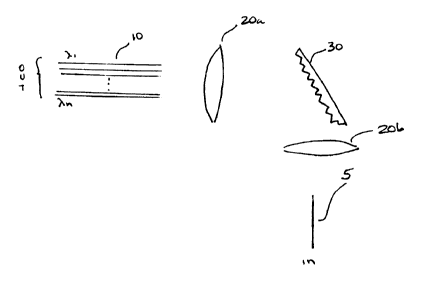
Referring now to Fig. 1 a an optical demultiplexor/ multiplexor is shown
operable in a
first direction and first mode of operation from the input fibre 5 labeled in
toward a
ribbon array of output fibres 10 as a demultiplexor. Disposed between the
input fibre S
and the output fibres 10 is a wavelength dispersive element in the form of a
grating 30
having etched high quality facets with well controlled side-wall angle and low
rounding.
Adjacent to and spaced a predetermined distance from the grating 30 is a lens
20 for
focusing dispersed diffracted light in the form of spots or sub-beams onto the
array I O of
output fibres such that each sub-beam couples with a particular optical fibre
of the array
of fibres 10. In operation, in the first demultiplexing mode of operation a
multiplexed
beam of light comprising a plurality of wavelengths ~,1.. ~,n is launched into
the input
optical fibre 5 and propagates through free space and impinges the grating 30
where it is
dispersed into sub-beams diverging at different angles depending upon
wavelength. The
lens 20 receives the diverging beams of light and focuses the beams at
different locations
along a plane where receiving ends of the waveguides 10 are located. In a
reverse
direction in a second mode of operation the optical circuit of Fig. 1 a
functions as a
multiplexor when separate beams having different wavelengths are launched into
the end
labeled OUT of the optical fibres 10. In this mode beams of wavelengths ~,1 to
~,n are
launched into separate fibres 10 and are directed onto the grating 30. The
beams are then
combined into a single beam that is directed to the optical fibre 5 labeled
IN.
Fig. lb is an alternative embodiment of the demultiplexor/multiplexor shown in
Fig. la.
In this alternative embodiment only a single lens 20a is required and optical
fibre l0a is
disposed adjacent to the array of fibres 10. In this embodiment alignment of
the input
fibre I Oa with the fibres 10 through reflection via the diffraction grating
30 can be made
by adjusting the angle of the diffraction grating 30 or/and, by varying the
distance of the
input fibre l0a and the fibres 10.
Turning now to Fig. 2, a graph of the output response of the
demultiplexor/multiplexor of
Fig. 1 is shown depicting the demultiplexing mode of operation. The graph
indicates the
8
CA 02281044 1999-08-27
Doc. No. 10-126 CA Patent
channel separation and bandwidth for wavelengths ~,1 to 7~n that are
demultiplexed. Fig. 5
in accordance with this invention shows a similar plot, however the bandwidth
is shown
to be greater than that shown in Fig. 2.
Fig. 3 is a detailed diagram of an array of optical fibres. The diameter of
each core in a
conventional single mode optical fibre is approximately l Opm. The diameter of
each
optical fibre 10 is approximately 125pm. Hence the separation between core
centres of
adjacent optical fibres is 125pm. As was previously stated the follow relation
hold
regarding core separation and bandwidth for a demultiplexor:
1 o bandwidth ~ core diameter
channel separation core separation
In order to increase the bandwidth of a grating based demultiplexor shown in
Fig. l, it is
necessary to lessen the core separation between adjacent optical fibres. An
embodiment
of this invention, which achieves this end, is shown in Fig. 4a, wherein a
concentrator
chip 40 is disposed between a grating 30 and an array of waveguides 10 and an
input or
output waveguide 10a. The concentrator chip 40 is a block of light
transmissive material
such as glass having waveguides disposed therein, arranged to fan out to a
dimension that
is compatible for directly coupling with the array of optical fibres 10,
hence, having cores
spaced 125pm apart. At an opposite end of the concentrator chip 40, the
waveguide ends
2o have cores that are much closer to one another; approximately l7pm apart;
the mode
field diameter of the cores being about l Opm and substantially constant
throughout the
concentrator chip. The waveguides within the concentrator chip can be provided
by ion
implantation or any other method that will enable a suitable refractive index
change
within the transparent substrate. The operation of the optical circuit shown
in Fig.4a is
similar to that of the circuit in Fig. lb, however, the lens is adapted to
provide focused
light beams at the end of the concentrator chip 40 (the right most end)
closest to the lens.
Although the circuit shown in Fig. 4a provides its intended function, an
alternative
embodiment shown in Fig. 4b overcomes limitations imposed by the embodiment of
Fig.
9
CA 02281044 1999-08-27
Doc. No. 10-126 CA Patent
4a. In the embodiment of Fig. 4a, the input optical fibre l0a and the output
optical fibres
are directly coupled with the concentrator chip 40 such that each fibre of the
array of
output fibres 10 and the input fibre l0a is coupled to a respective waveguide
within the
concentrator chip. Each of the waveguides in the exemplary embodiment shown in
Fig.
5 4a in the concentrator chip 40 has a core diameter of about 10 ~.m. and the
separation
between cores at one end is approximately 17 Vim. Since this these dimensions
are fixed
once the chip is fabricated, there is little or no possibility of adjusting
the interchannel
spacing of the demultiplexed channels demultiplexed by the device. However, in
the
preferred embodiment shown in Fig. 4b, the optical fibre l0a is separate from
the
to waveguides within the concentrator chip 40 and is separate from the
concentrator chip 40.
Most importantly, this arrangement allows for fine-tuning of the
demultiplexor/multiplexor by varying the mode field diameter (MFD) of the core
of the
optical fibre 10a. As the MFD of the optical fibre is lessened, the channels
become
slightly narrower, and conversely as the MFD of the optical fibre l0a is
increased, the
channels become slightly wider. Hence keeping the input/output optical fibre
l0a
separate from the concentrator chip as is shown in Fig. 4b, allows for fine
tuning of the
demultiplexor/multiplexor without discarding, redesigning, and remanufacturing
the
concentrator chip 40. This is a significant advantage in the manufacture of
these devices.
Furthermore, if an optical fibre l0a having a very large MFD is used in a
system having
2o very narrow closely spaced channels, the device can function as a
multiplexor/splitter by
broadening the bandwidth of the channels such that they overlap.
Fig. 5 illustrates the output response of the circuit of Fig. 4a used in a
demultiplexing
mode of operation. Here the bandwidth is shown to be wider than in Fig. 2.
Numerous other embodiments may be envisaged without departing from the spirit
and
scope of the invention. For example, the in/out waveguide shown in Fig. 5 can
alternatively be disposed appropriately at the end of the device adjacent to
and at a non-
zero angle to the array of optical fibres 10.
to