Note: Descriptions are shown in the official language in which they were submitted.
CA 02281788 1999-08-16
METHOD OF PRODUCING SILICON OXIDE FILM, METHOD OF
MANUFACTURING SEMICONDUCTOR DEVICE, SEMICONDUCTOR
DEVICE, DISPLAY, AND INFRARED IRRADIATING DEVICE
Technical Field
The present invention relates to a method for manufacturing a silicon oxide
film of
good quality by a vapor deposition method. This silicon oxide film is suitable
for an
underlying layer-protecting film, a gate insulating film, an inter-dielectric
film, etc. The
present invention also relates to a method for manufacturing a micro-
semiconductor
device of good quality (for example, metal/oxide film/semiconductor field
effect transistor
(MOSFET)) wherein a semiconductor surface is oxidized at a relatively low
temperature
of, e.g., about 800 C or less and an extra-thin silicon oxide film (having
less than about
10nm in film thickness) of good quality is then formed. The present invention
also
relates to a method for manufacturing a semiconductor device (for instance, a
thin film
transistor) of high performance and reliability at a relatively low
temperature such as
around 600 C or below. Moreover, the present invention relates to a
semiconductor
device of high performance and reliability manufactured thereby, and a display
device
(such as a liquid crystal display device) of high performance and reliability
equipped with
this semiconductor device. Furthermore, the present invention relates to an
infrared
light irradiating device for manufacturing a silicon oxide film of good
quality.
Background Technology
Silicon oxide films are widely used for gate insulating films of polycrystal
silicon
thin-film transistors (p-Si TFT) and gate insulating tilms of micro-
semiconductor devices,
1
CA 02281788 1999-08-16
such as VLSI having an extra-thin oxide film and the like, etc. The quality of
these
silicon oxide films has important effects on the electric characteristics of
these
semiconductor devices.
When a silicon oxide film is used for a gate insulating film of low
temperature p-Si
TFT, it is necessary to form a silicon oxide film at a relatively low
temperature such as
around 600 C or below at which a general glass substrate can be used. Thus, a
chemical
vapor deposition method (CVD method) and a physical vapor deposition method
(PVD
method) have been conventionally applied.
Moreover, in manufacturing a micro-semiconductor device such as VLSI having an
ultra thin oxide film, an ultra-thin silicon oxide film is provided by
thermally oxidizing
silicon at a relatively low temperature of e.g., 800 C or below under an
atmosphere
containing oxygen and hydrochloric acid, or by irradiating a silicon substrate
with oxygen
plasma, etc.
However, these conventional silicon oxide films have a problem in that the
film
quality is extremely low since electric charge trapped in oxide films is
large, and the like.
As a result, if a conventional silicon oxide film is used as a gate insulating
film of
p-Si TFf, there is a problem in that only a p-Si TFT of low quality and
reliability can be
provided. This is because it is easy to vary flat band voltage (Vtb) of a
semiconductor
device since silicon oxide films have a large amount of fixed electric charge
of an oxide
film, to enlarge threshold voltage (Vth) since a surface trapping level is
high, and to
introduce electric charge into oxide films since an oxide film trapping level
is large, etc.
In other words, conventional semiconductor devices such as p-Si TFT have many
problems because the quality of silicon oxide films is low.
2
CA 02281788 1999-08-16
The same problems are found in a micro-semiconductor device such as VLSI with
an ultra-thin silicon oxide film. Ultra-thin silicon oxide films are generally
formed at a
relatively low temperature of around 800 C or below, so that they have all the
problems
of low temperature oxidation. More specifically, the problems are that a
surface level
and an oxide film trapping level are extremely high and the current of an
oxide film is
large. These problems are the main causes in limiting the properties of a
super-
integrated circuit and shortening its life.
Thus, the present invention solves the above-mentioned problems, and its
objectives are to present a method for manufacturing a silicon oxide film of
high quality
by a vapor deposit method, to present a method for manufacturing a micro-
semiconductor device such as VLSI having an ultra-thin oxide film of high
quality by
applying a silicon oxide film formed at a relatively low temperature such as
about
800 C or below, to present a method for manufacturing a semiconductor device
(for
instance, a thin film transistor) of high performance and reliability at a
relatively low
temperature of e.g., 600 C or below, to present such a semiconductor device of
high
performance and reliability and a display device, and to present a device for
manufacturing a silicon oxide film of high quality.
Disclosure of the Invention
The present invention, first as a step of forming a silicon oxide film,
deposits a
silicon oxide film on various substrates such as an insulating substrate (for
example,
quartz glass substrate, general non-alkali glass substrate, and the like), a
semiconductor
substrate (for instance, monocrystal silicon substrate, compound semiconductor
substrate, etc.) and a metal substrate by a vapor deposition method (for
instance,
3
CA 02281788 1999-08-16
chemical vapor deposition method (CVD method), physical vapor deposition
method
(PVD method), and the like). A silicon oxide film is also formed by the
oxidation of a
semiconducting material surface such as by heat treatment (thermal
oxidization) of a
semiconducting material surface under an oxidizing atmosphere, the plasma
irradiation
(plasma oxidization) of an oxide material (such as oxygen and dinitrogen
monoxide) to a
semiconducting material surface, the supply of ozone(O,) (ozone oxidization),
the supply
of active oxygen (active oxygen oxidization) generated by a heated metal
catalyst, or the
like.
In the step of forming a silicon oxide film, a silicon oxide film is formed
directly
on a semiconductor substrate or a glass substrate as a field oxide film, a
gate insulating
film, an inter-dielectric film, an underlying layer-protecting film, or the
like.
Furthermore, a silicon oxide film is formed on a semiconductor film after
forming the
semiconductor film having silicon as a simple substance or as a main substance
on an
insulating material such as an oxide film formed on the surface of a glass
substrate or a
monocrystal silicon substrate as the step of forming a semiconductor film.
The semiconductor film having silicon as a main substance contains a mixture
of
silicon and other elements such as germanium in the film, and contains silicon
at about
80% or above in construction ratio. Also, the semiconductor films having
silicon as a
simple substance include semiconductor films with silicon containing
impurities such as P,
B, Al, As and the like. Therefore, the silicon oxide films in the present
invention mean
not only pure silicon oxide films (SiOx films wherein x is roughly 2) but also
silicon oxide
films containing these elements and the oxides thereof. Silicon materials are
in a
4
CA 02281788 1999-08-16
monocrystal state, polycrystal state,-amorphous state, mixed crystal state
that is polycrystal and amorphous, and the like.
The oxide tilm deposition step by a vapor deposition method is carried out at
a
relatively low temperature around 600 C or below. A sputtering method,
evaporation
method, and the like can be applied to a PVD method. Also, as for a CVD
method, an
atmospheric pressure chemical vapor deposition method (APCVD method), low
pressure
chemical vapor deposition method (LPCVD method), plasma chemical vapor
deposition
method (PECVD method), and the like are applicable.
The step of forming an oxide film by thermal oxidation is carried out by
treating a
semiconducting material in the temperature range from around 600 to 1,000 C
under an
oxide atmosphere containing oxygen, water vapor, hydrochloric acid, etc. In
forming an
ultra-thin oxide film at less than about lOnm in film thickness, thermal
oxidation is often
carried out under the temperature around 800 C or below. Also, in the step of
forming an oxide film by plasma oxidation, ozone oxidation, active oxygen
oxidation or
the like, a semicondueting material is treated under the condition about 600 C
or
below. (In this specification, thermal oxidation, plasma oxidation, ozone
oxidation and
active oxygen oxidation temperatures around 800 C or below is called the low
temperature oxide method hereinafter.) The silicon oxide film obtained by the
low
temperature oxidation method generally has low quality in comparison with a
thick
thermal oxide film (in thickness of around 50nm or above) obtained at the
temperature of
around 1,100 C or above.
Next, in the present invention, the quality of these silicon oxide films will
be
improved by the following infrared light irradiation step. In the infrared
light irradiation
CA 02281788 1999-08-16
step, infrared light is irradiated onto'a silicon oxide film obtained by the
above-noted
vapor deposition method and an ultra-thin silicon oxide film obtained by the
low
temperature oxide method. The irradiation infrared light is absorbed by the
silicon oxide
film, increasing the temperature of the oxide film. Due to this temperature
increase, the
improvement in quality of the silicon oxide film itself and a surface would
accelerate.
The transmitted light intensity I of infrared light to the silicon oxide film
is:
I=1loexp(-k-t) where incident light intensity is Io, the film thickness of a
silicon oxide film
is t (cm), and the absorption coefficient of infrared light by the silicon
oxide film is k(cm-
`). When a substrate is made of a material having the same optical
characteristics
equivalent to that of a silicon oxide film such as glass, or when the
absorption coefficient
to the irradiation infrared light is made of a material larger than the
silicon oxide film,
irradiation infrared light is absorbed not only by a silicon oxide film but
also by a substrate
such as glass. Thus, if an absorption factor at a silicon oxide film is too
low, the
temperature of a silicon oxide film will not effectively increase but rather
infrared light
will be absorbed mainly by a substrate, thereby damaging the substrate. In
other words,
the substrate will be cracked or warped. Therefore, the temperature increase
by infrared
light is expected to be large at a silicon oxide film and small at a substrate
such as glass.
The maximum film thickness of a silicon oxide film of the present invention is
around
1Eim, and other substrates such as glass substrates normally have a thickness
of about
several hundred m or above. Thus, when the absorption of infrared light on a
silicon
oxide film exceeds around 10% with respect to incident light, the absorption
on a
substrate will be less than around 90%. In this case, the thickness of a
silicon oxide film
and a substrate is different by several hundred times or above, so that the
temperature
6
CA 02281788 1999-08-16
increase of a substrate will be much'lower than the temperature increase of a
silicon oxide
tilm. Since infrared light enters a substrate after being irradiated from the
surface
thereof and then passes through an oxide film, it is understood that
k=t > 0.1
in accordance with the formula above shall be satisfied so as to have less
than about 90%,
of transmitted light from a silicon oxide film. When a substrate has a much
smaller
absorption coefficient to infrared light, like a monocrystal silicon, than the
absorption
coefficient of a silicon oxide film, the chance of damaging the substrate is
small even if the
absorption of infrared light on a silicon oxide film is extremely small, so
that it is possible
to obtain
k=t > 0.01.
As described herein, in order to improve film quality by irradiating infrared
light
onto a silicon oxide film, the silicon oxide film has to absorb infrared
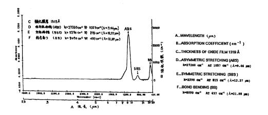
light. FIG. 1
shows the infrared light absorption characteristics of a silicon oxide film
deposited by
electron cyclotron resonance plasma chemical vapor deposition method (ECR-
PECVD
method). The left vertical line expresses Absorbance (a) of an oxide film, and
the right
vertical line indicates Absorption Coefficient k(cm-l). The correlation of
k = ln(10)=a/t
is found between Absorbance (a) and Absorption Coefficient k. However, t (cm)
is a
film thickness of a silicon oxide film. The horizontal line in FIG. 1 is the
wave number
(cm-i) of infrared light and the wavelength ( m) of corresponding light.
There are generally three types of absorption peaks in a silicon oxide film
for
infrared light: ABS (asymmetric bond stretching peak), SBS (symmetric bond
stretching
7
CA 02281788 1999-08-16
peak) and BB (bond bending peak). As clearly seen from FIG. 1, ABS has the
absorption coefficient of 27,260cm-` at the wave number of around 1,057cm-`
(9.46Erm in
wavelen(yth). SBS has the absorption coefficient of 2,290cm-` at the wave
number of
around 815em-` (12.27tim in wavelength). BB has the absorption coefficient of
8,090cm"1 at the wave number of about 457cm"' (21.88Ftm in wavelength). The
wavelength of irradiated infrared light can be adjusted to these three types
of absorption
pe4ks. Thus, the wavelength of infrared light can be between around 8.929 m
(1,120cm-' in wave number) and about 10 m (1,000cm-` in wave number) to be
absorbed
at ABS; the wavelength of infrared light can be between around 11.364Ftm
(880cm-` in
wave number) and about 13.158 m (760cm-' in wave number) to be absorbed at
SBS;
and the wavelength of infrared light can be between around 19.231 m (520cm-`
in wave
number) and about 25Erm (400cm-` in wave number) to be absorbed at BB.
Infrared light is most effectively absorbed at ABS having the largest
absorption
coefficient. Even the silicon oxide film having the lowest quality provided by
a vapor
deposition method has about 25,000cm-` in absorption coefficients at ABS.
Thus, in
order to satisfy the above-noted correlation of absorption coefficients and
oxide film
thickness for all the silicon oxide films obtained by a vapor deposition
method, the
thickness of a silicon oxide film may be about 40nm or above. Similarly, when
a
monocrystal silicon substrate is oxidized about 800 C or below, the absorption
coefficient of an oxide film is about 30,000cm-` or above, so that it will be
possible to
improve film quality of an ultra-thin oxide film without damaging a substrate
if an oxide
film thickness is about 3.3nm at minimum or above.
8
CA 02281788 1999-08-16
In other words, the infrared libht irradiated onto a silicon oxide tilm in the
present
invention should contain a wavelength component to be absorbed by the silicon
oxide
film. Moreover, the light may contain a wavelength component that is not
absorbed by
the silicon oxide film, but the ratio should preferably be as small as
possible so as to
reduce damage to a substrate and a semiconductor film. In other words, it is
preferable
that the infrared light irradiated to the silicon oxide film in the present
invention contains a
wavelength component to be absorbed by the silicon oxide film as a main
component.
Moreover, it is more preferable that the infrared light irradiated onto a
silicon oxide
film in the present invention particularly contains a wavelength component
that
corresponds especially to asymmetrical bond stretching vibration of the
silicon oxide film
in wavelength components to be absorbed by the silicon oxide film. Since it
has a large
absorption coefficient, it is particularly effective to heat the silicon oxide
film. It may
not contain a wavelength component that does not correspond to asymmetrical
bond
stretching vibration of the silicon oxide film, but it is preferable that the
ratio is as small as
possible with respect to the heating efficiency of a substrate. In other
words, it is
preferable that the infrared light irradiated onto the silicon oxide film in
the present
invention contains a wavelength component, which corresponds to the
asymmetrical bond
stretching vibration of the silicon oxide film, as a main component.
In the above-described aspects, the infrared light irradiated to a silicon
oxide film in
the present invention preferably contains the wavelength component of about
8.9trm or
above to around 10ttm or less; and more preferably, it contains the wavelength
component of about 8.9Erm or above to around 10 m or less as a main component.
9
CA 02281788 1999-08-16
In order to satisfy such a request, the laser beams having a wavelength at
about
ABS of an oxide tilm may be irradiated as infrared light. Since the laser
beams oscillate
in a narrow wavelength range, it is possible to reduce the irradiation of
light in
wavelength, which does not heat a silicon oxide film, to a substrate and a
semiconductor
film as much as possible. As such laser beams, the most excellent are carbon
dioxide
(CO,) laser beams, and best among these are carbon dioxide (CO,) laser beams
of around
9.3,hm in wavelength. The carbon dioxide (CO,) laser beams of around 9.3Erm in
wavelength will be explained later.
The carbon dioxide laser beams have many oscillation lines in a waveband from
8.9tLm (1,124cm-` in wave number) to 11Etm (909cm-` in wave number) as
represented by
the wavelength of 9.3055 0.0005 m (1,074.63 0.05cm"' in wave number); and
these
wave numbers of light almost match ABS of the silicon oxide films obtained by
a vapor
deposition method and at a relatively low temperature of about 800 C. FIG. 14
is a
table showing the oscillation lines of a carbon dioxide laser beam which can
be used in the
present invention. The fluctuation of wavelength of each oscillation line is
only
0.0005 m and is only 0.05cm-` in wave number. Among these oscillation lines,
the
oscillation line particularly suited for irradiated infrared light is the one
which is strongly
absorbed by almost all the silicon oxide films and having the wavelength from
about
9.2605 0.0005Erm (1,079.85 0.05cm-1 in wave number) to the wavelength of about
9.4885 0.0005 m (1,053.91 0.05cm-1 in wave number). (These carbon dioxide
laser
beams are called carbon dioxide laser beams around the wavelength of 9.3Fim
(1,075cm-`
in wave number).)
------ ------
CA 02281788 1999-08-16
As film quality declines, the location of ABS of a silicon oxide film shifts
to the side
of lower wave number. ABS of the silicon oxide film obtained by a vapor
deposition
method actually has the wave number of infrared light at about 1,055cm-' to
around
1,070cm-`, and this value almost matches the wave number of carbon dioxide
laser beams
around the wavelength of 9.3Erm (1,075cm-' in wave number). In addition, the
half
value width of ABS of such a low quality film is likely to increase, often
reaching 100cm-
Thus, even if ABS fluctuates slightly from the wave number of carbon dioxide
laser
around the wavelength of 9.3Ftm, a silicon dioxide tilm can sufficiently
absorb carbon
dioxide laser beams. As oxide film quality improves by the irradiation of a
carbon
dioxide laser beam, the half value width decreases. However, since ABS also
shifts to
the side of higher wave numbers, the oxide film can still absorb a carbon
dioxide laser
beam around 9.3Eim in wavelength efficiently. When a silicon oxide film is
obtained by
oxidizing a monocrystal silicon substrate, the quality of an oxide film is
high at the oxide
temperature of about 1,100 C or above, so that ABS is at around 1,081cm-1.
Below
about 1,100 C of oxidation temperature, the location of ABS shifts to the side
of lower
wave numbers at the rate of about 2cm-` as the oxidation temperature declines
by 100 C,
and will be at 1,075cm-1 in the oxidation at 800 C. This value matches the
wave number
of carbon dioxide laser beams of 9.3 m in wavelength, and it is understood
that a carbon
dioxide laser beam at around 9.3Eim in wavelength is ideal as irradiated
infrared light.
An irradiated laser beam can oscillate a single beam having a wavelength at
around 9.3trm
such as the wavelength of 9.3055 0.0005Erm, or can oscillate a plurality of
light having
wavelengths at around 9.3Etm at the same time.
11
CA 02281788 1999-08-16
It is preferable to carry out heat treatment for a long period at a high
temperature in
order to improve the quality of an oxide film by infrared light irradiation.
According to
an experiment, if a one-time infrared light irradiation period is less than
about 0.1
seconds, the quality improvement of an oxide film will be clear after the
temperature of an
oxide film exceeds about 800 C. Thus, if infrared light irradiation is carried
out so as to
set the temperature of an oxide film at about 800 C or above for a period of
about 0.1
sec,pnds, the quality of the oxide film will certainly improve. The
correlation between
the temperature and period necessary for improving the quality of an oxide
film
establishes the relation that the treatment period is shortened by one digit
as the oxide
film temperature increases by 50 C. Thus, with the optional oxide film
temperature T X
( C) due to raising the oxide film temperature by infrared light irradiation
to the oxide
film to around 800 C or above and the total time (z (s)) at that temperature
(T X), T x and
i satisfy the correlation:
i > exp(ln(10)=(b=T X+15)); and
b=-0.02 ( C`).
In other words, the quality of an oxide film will improve if infrared light is
irradiated to
the film under the condition where T x satisfies the relations:
Formula (1): i > exp(-0.04605=T x+34.539).
As a result, oxide film current decreases; withstand voltage rises; oxide film
fixed charge
decreases; and oxide film protection levels are reduced.
When a silicon oxide film is formed on a semiconducting material having
silicon as
a simple substance or a main substance, infrared light irradiation of the
present invention
can improve the quality of an oxide film as well as interface characteristics
between a
12
CA 02281788 1999-08-16
semiconductor and a dielectric film: Either by vapor deposition method or low
temperature oxide method, large oxidation stress always remains at the
interface between
a semiconductor film and an oxide film right after the oxide film is formed.
An oxide
film grows under this mechanism: in the low temperature oxidation of a
semiconductor
(for instance, Si), oxidation reactants (for example, O,) are diffused in an
oxide film (for
instance, SiO,), and the reactants supply oxygen atoms(O) between the atoms of
the
semiconductor (e.g., between Si-Si) after the reactants reach the interface
between the
oxide film and the semiconductor film, thus forming a new oxide film (for
example, Si-0-
Si). As a result, the interatomic distance of adjacent atoms in a
semiconductor (for
example, distance between Si-Si) becomes clearly different from the
interatomic distance
of a semiconductor in an oxide film with an oxygen atom in-between (for
instance,
distance between Si and Si in Si-O-Si). This difference in interatomic
distances
generates tensile stress in a semiconductor film and compressive stress in an
oxide film.
If oxidation temperature is sufficiently high (around 1,070 C or above), an
oxide film will
have viscous flow and the stress generated by oxidation will be relaxed.
However, if the
oxidation temperature is below about 1,070 C, the stress relaxation time will
become
much longer, so that the stress generated by oxidation will not be relaxed and
remains in
both thin films with an interface there-between.
Similar matters occur when an oxide film is formed by a vapor deposition
method.
That is because, in the extremely early stage of oxide film deposition,
oxidation
accelerating materials used for a vapor deposition method (O,, 03 or the like)
enter
between atoms of a semiconductor, forming an ultra-thin oxide film of about
0.5nm to
about 2.Onm and then depositing an oxide film by the vapor deposition method
onto the
13
CA 02281788 1999-08-16
ultra-thin oxide hlm. As described above, the vapor deposition method is
carried out under the temperature 600 C or below, so that oxidation stress
during the period of
ultra-thin oxide film formation cannot be relaxed. Regardless of whether it is
a
monocrystal film or a polycrystal film, oxidation stress fluctuates grid
intervals between
atoms in a semiconductor; therefore, a trapping level for electrons and
electron holes is
formed at an interface between a semiconductor film and an oxide film, thus
reducing the
mobility of charge carriers (electrons in a conduction band and electron holes
in a valence
band) at a surface at the same time. In the present invention, oxidation
stress at an
interface between a semiconductor film and an oxide film is relaxed by raising
the
temperature of an oxide film locally by infrared light irradiation, thereby
forming an
interface of good quality.
There are suitable conditions for improving an interface by infrared light
irradiation. FIG. 2 is a graph showing the relations between stress relaxation
time
(vertical line) and heat treatment temperature (horizontal line) calculated in
reference to
Irene's theory regarding a silicon oxide film (E.A. Irene et al.: J.
Electrochem. Soc. 129
(1982) 2594). For example, when heat treatment temperature is 1,230 C, the
viscous
flow of an oxide film begins from a heat treatment time of about 0.1 seconds
or longer
and oxidation stress is released. Thus, for the quality improvement of an
interface by
infrared light irradiation, irradiation conditions can be set so as to satisfy
the conditions
above the curve shown in FIG. 2 (in the range described as an infrared light
irradiation
effective area in FIG. 2). More specifically, with the optional oxide film
temperature T x
( C) due to raising the oxide film temperature by infrared light irradiation
to the oxide
14
CA 02281788 1999-08-16
film to 1,000 C or above and the total time (i (s)) at that temperature (T X),
T,,X and T satisfy the correlation:
z > 2=(l+v)=YI/E; and
tl=rlõ=exp(e/(k=(Tox+273.15))).
In other words, infrared light may be irradiated under the condition with
T,,x, satisfying
the relations:
Formula (2): i> 2=(l+v)=>7õ=exp(s/(k=(T X+273.15)))/E: where v is the
Poisson's ratio of
an oxide film; E is the Young's modulus thereof; rl is the viscosity thereof;
rlo is the pre-
exponential factor of viscosity; s is the activation energy of viscosity; k is
Boltzmann's
constant; and each has the following numbers respectively:
v=0.18;
E=6.6x10" dyn cm ';
r1o=9.549x10-" dyn=s=cm-';
s=6.12eV; and
k=8.617x10⁻⁵ eV=IC`.
In order to complete heat treatment by infrared light onto an oxide film
without
damaging a substrate and a semiconductor film, the time for heating the same
point on the
substrate is preferably less than about 0.1 seconds. This is because, based on
the
experience of rapid thermal agitation (RTA) treatment, such a problem will not
occur by a
short time treatment of less than 0.1 seconds, while a glass substrate will
warp or break
during a heating time of about one second at the temperature of around 800 C
or above.
If T X is about 1,230 C or above, it is possible to set one-time irradiation
for shorter than
0.1 seconds, but this condition cannot be satisfied with one-time irradiation
around
CA 02281788 1999-08-16
1,230 C or below. Therefore, in order to improve interface characteristics
under the
condition of infrared light irradiation around 1,230 C or below of T x,
infrared light may
be irradiated so as to let i satisfy the above-noted inequality by setting the
time of one-
time irradiation shorter than around 0.1 seconds and by repeating this
irradiation several
times. In this sense, discontinuous oscillation with periodicity is more
preferable than
continuous oscillation.
, The discontinuous oscillation of infrared light having periodicity is as
shown in an
elapsed time figure shown in FIG. 3. One period of infrared light consists of
oscillation
time (toN) and non-oscillation time (toFF). In order to minimize thermal
distortions to
materials other than an oxide film such as a semiconductor, it is expected to
equalize the
oscillation time to the non-oscillation time or shorten the oscillation time
to the non-
oscillation time (toN s taFF). This is because radiation will certainly be
promoted since
the oscillation time is shorter than the non-oscillation time. Furthermore, in
consideration of productivity, it seems ideal if the oscillation period and
the non-
oscillation period are roughly the same.
One more matter that requiring attention regarding irifrared light irradiation
is that
the control of the maximum achievable temperature of an oxide film is expected
to be
the melting point of a semiconducting material or below when an oxide film is
formed on
a semiconducting material as a gate dielectric film or an inter-dielectric
film to irradiate
infrared light onto the oxide film. For instance, when the semiconducting
material is
intrinsic silicon or silicon containing a small amount of impurities (less
than about 1% of
impurity concentration), the melting point of silicon is about 1,414 C. Thus,
the
maximum achievable temperature of an oxide film by infrared light irradiation
is
16
CA 02281788 1999-08-16
preferably below about 1,414 C. This is because as a semiconducting material
melts,
adverse phenomena will occur: the change in an impurity concentration in a
semiconductor or the increase in random reconfiguration of an interface
between an oxide
film and a semiconductor, which then result in the increase in an interface
level, and, as
the worst case, the evaporation and drift of the semiconducting material, thus
breaking
down a semiconductor device, etc. In order to avoid these phenomena so as to
manufacture an excellent semiconductor device with stability, the maximum
achievable
temperature of an oxide film can be set to the melting point of a
semiconducting material
or below.
When a semiconducting material is in a polycrystal or amorphous state,
dangling
bonds are found in the semiconductor, and it is preferable that these dangling
bonds are
terminated by atoms such as hydrogen (H), tluorine (F). Dangling bonds form
trapping
levels for the electrons and electron holes at a deep level in a forbidden
band-gap (near
the center of the forbidden band-gap), and reduce the number of electrons at a
conduction
band and the number of electron holes at a valence band. At the same time,
charge
carriers are scattered, thus reducing mobility. Through such a principle,
dangling bonds
reduce semiconductor characteristics. The temperature increase of an oxide
film due to
infrared light irradiation improves the quality of a silicon oxide film itself
and an interface
significantly; and at the same time, there is a fear that the hydrogen or
fluorine which
terminated dangling bonds will be removed by heat conduction to a
semiconducting
material. Thus, in order to prepare an excellent semiconductor device such as
a solar
battery with a high light transforming efficiency and a thin-film transistor
for high speed
operation at low voltage, it is preferable to carry out a step of terminating
dangling bonds
17
CA 02281788 1999-08-16
by hydrogen plasma irradiation or the like after infrared light irradiation.
Due to this
step, the number of danbling bonds generated by infrared light irradiation
will be reduced;
the number of charge carriers will increase; and at the same time, the
mobility will
improve.
In the infrared light irradiation in the present invention, the heating time
of the same
point on an oxide film by one-time irradiation is preferably less than about
0.1 seconds
anq is short. By such a short-time irradiation, not only will thermal damage
to a
substrate be prevented, but also the diffusion of vapor reactive to a
semiconducting
material such as oxygen through an oxide film from a vapor phase will be
extremely small,
so that the irradiation atmosphere can be air. If the irradiation time is
long, oxygen in
the air will diffuse to an interface, so that there is a fear that a new low-
temperature oxide
film will be formed during the cooling step of a semiconducting material. As a
result, no
quality improvement of interface characteristics will occur. In this sense,
the irradiation
atmosphere is preferably inactive vapor such as nitrogen, helium and argon.
Due to
infrared light irradiation, the surface of a semiconducting material will be
heated up to
near the melting point, so that a noble gas such as helium and argon is more
preferable as
the irradiation atmosphere than nitrogen with nitriding capability. By doing
this, there
will be no limitation on the infrared light irradiation time as long as a
substrate or
semiconducting material is not damaged, and a good interface will be obtained.
This
irradiation atmosphere control will be especially important to an ultra-thin
oxide film to
which diffusion is easy.
In the method of manufacturing a semiconductor device of the present
invention, as
a semiconductor film has the structure of a thin crystalline film of less than
about 200nm
18
CA 02281788 1999-08-16
in film thickness sandwiched between silicon oxide films, the electric
characteristics of the
semiconductor device will clearly improve. The semiconductor device having
this
structure has two interfaces - an interface between a semiconductor film and a
top oxide
film and an interface between a semiconductor film and a bottom oxide film.
When
impurities are added to a semiconductor film as donors or acceptors and the
film is used
as wiring, both these interfaces will contribute to electric conduction. Also,
as a
serpiconductor film is used as an active layer of a silicon-on-insulator (SOI)
semiconductor device, the thin semiconductor film as a whole will be depleted,
so that
both interfaces impact upon electric characteristics. By the irradiation of
infrared light
to this structure, the oxide films sandwiching the top and bottom of the
semiconductor
film will be heated by infrared light irradiation; as a result, the quality of
both interfaces
will improve. Moreover, as the crystalline semiconductor film is polycrystal,
the
semiconductor film will be natually heated by heat conduction from the top and
bottom
oxide films and even a polycrystalline semiconductor film will recrystallize.
Due to this
recrystallization, crystal grains of the polycrystal semiconductor film will
become large
and the number of defects in the semiconductor film will decrease, so that
semiconductor
characteristics will further improve.
As described above, the present invention can improve conventional silicon
oxide
films of low quality (silicon oxide films formed by vapor deposition method,
ultra-thin
oxide films obtained by low-temperature oxide method) to films of good quality
by
adding the step of infrared light irradiation; and at the same time, the
present invention
can improve interface conditions between a semiconductor and an oxide film.
Moreover, when a semiconductor film is sandwiched between a first oxide film
and a
19
CA 02281788 1999-08-16
second oxide film, both interfaces can be improved. Furthermore, when the
semiconductor is a crystalline tilm, this crystal can also he improved. As a
result,
superior effects will be realized: the electric characteristic of a
semiconductor device,
represented by a thin-film transistor, will increase; and at the same time,
the operational
stability and reliability of the semiconductor device will be enhanced.
Brief Description of the Drawing
FIG. 1 is a figure showing the infrared light absorption characteristics of a
silicon
oxide film. FIG. 2 is a figure showing the effective area of the present
invention. FIG.
3 is an elapsed time figure explaining infrared light oscillation. FIG. 4 is a
figure
showing the change in oxide film temperature by infrared light irradiation.
FIG. 5 shows
tigures explaining the method of manufacturing a semiconductor device of the
present
invention. FIG. 6 is a figure explaining a display device of the present
invention. FIG.
7 is a figure explaining an infrared light irradiating device of the present
invention. FIG.
8 is a tigure explaining an infrared light irradiating device with a fly eye
lens of the present
invention. FIG. 9 is a figure showing the principle of leveling an infrared
light intensity
distribution with the application of a fly eye lens. FIG. 10 is a figure
explaining an
infrared light irradiating device with a Fourier-transform phase hologram of
the present
invention. FIG. 11 is a figure showing the principle of leveling an infrared
light intensity
distribution with the application of a Fourier-transform phase hologram. FIG.
12 is a
tigure explaining an infrared light-irradiating device with a galvano-scanner
of the present
invention. FIG. 13 is a figure explaining an infrared light-irradiating device
with a
polygon mirror of the present invention. FIG. 14 is a table showing an
oscillation lines
of carbon dioxide (CO2) laser.
CA 02281788 1999-08-16
Best Mode of Execution of the Claimed Invention
The semiconductor device of the present invention includes at least a
semiconductor film formed on a first silicon oxide tilm as a dielectric
material and a
second silicon oxide film formed on this semiconductor film. If it is a top-
gate type
semiconductor device, the first silicon oxide film corresponds to an
underlying layer-
protecting film and the second silicon oxide film corresponds to a gate
dielectric film.
On the other hand, if it is a bottom-gate type semiconductor device, the first
silicon oxide
film corresponds to a gate insulating film and the second silicon oxide film
corresponds to
an inter-dielectric film. Moreover, the display device of the present
invention has such a
semiconductor device.
A substrate is first prepared for fabricating these semiconductor and display
devices. As the substrate, glass, monocrystal silicon, and the like are
generally known,
but even a substrate besides these can resist high temperature during the
manufacturing
process of a semiconductor device. Moreover, if the mixture of impurities into
a
semiconductor film is sufficiently small, the type or size thereof will not be
questioned.
First, the first silicon oxide film is formed on a substrate by vapor
deposition
method or low temperature oxidation method. If the substrate is highly pure
quartz
glass, a quartz glass substrate can also be used for the first silicon oxide
film.
Next, a semiconductor film is formed on a dielectric material where at least a
surface in contact with the semiconductor film is the first silicon oxide
film. In this step
of forming a semiconductor film, a high energy body such as a laser beam and
heat is
supplied to this semiconductor film after film deposition by vapor deposition
method or
the like, thus accelerating the molten crystallization and then the solid
phase
21
CA 02281788 1999-08-16
crystallization of the semiconductor-tilm. If the initially deposited thin
film is amorphous
or the mixed crystal which is a mixture of amorphous and microcrystal, this
step is
generally called crystallization. On the other hand, if the initially
deposited thin film is
polycrystal, this step is normally called recrystallization. In this
specification, both are
called crystallization and are not distinguished from each other. The most
excellent high
energy bodies are the krypton t7urine (KrF) excimer laser and xenon chlorine
(XeCI)
excimer laser. Due to the irradiation thereof, at least the surface of a
semiconductor thin
film is molten and crystallized. There is an excellent characteristic in that
crystal grains
within a molten range rarely have defects by molten-crystallization. On the
other hand,
the control of the energy supplied during molten-crystallization is highly
difficult: if the
irradiation energy density of the excimer laser or the like onto the
semiconductor thin film
is slightly larger than an appropriate level, it is realized that the diameter
of crystal grains
of the polycrystal film is suddenly reduced from 1/10 to 1/100 and, in the
worst case, the
semiconductor film will disappear. Therefore, in the present invention, the
molten-
crystallization of a semiconductor film is carried out by setting an
irradiation laser energy
density lower than an appropriate level by about 5mJ=em-2 to about 50mJ=cm-2.
As a
result, the molten-crystallization of a semiconductor film will be carried out
with stability.
Of course, the crystallization of a polycrystal semiconductor film remains
insufficient
under this condition; however, there is a step of irradiating infrared light
to the oxide film
as the following step in the present invention.
In other words, on the crystalline semiconductor film obtained thereby, a
second
silicon oxide film is formed by vapor deposition method or low temperature
oxidation
22
CA 02281788 1999-08-16
method, and a light irradiating step where infrared light is irradiated to the
second silicon
oxide film after this step of forming the oxide film is then provided.
As a silicon oxide film is heated by infrared libht irradiation, even the
semiconductor film is heated at the temperature near a semiconductor molten
temperature
for a relatively long period of several s to several ms. In the above-
described molten-
crystallization, the semiconductor film is heated at the molten temperature
for several
do~en ns. In comparison to this, the semiconductor temperature during the
light
irradiation step is slightly lower. However, the heating process time extends
a hundred
to a million times, so that the crystallization of a semiconductor film that
is insufficient
only by molten-crystallization will be significantly improved in the libht
irradiation step.
Durinb the molten-crystallization step, crystal grains of high quality are
formed only near
the surface of a semiconductor film, and a large amount of fine defects and
amorphous
components remain in the bottom section of the semiconductor film near the
first oxide
film. These residual components are crystallized from the crystal grains of
good quality
near the surface in the light irradiation step, and a crystallized film of
good quality is then
formed over the entire film thickness direction of the semiconductor film. As
understood from such a principle, the semiconductor film being sandwiched
between the
first oxide film and the second oxide film means that the semiconductor film
is heated
from both top and bottom in the light irradiation step; as a result, uniform
crystallization
is promoted over the entire semiconductor film. Similar results found in the
molten-
crystallized film are found when the semiconductor film is crystallized in a
solid phase.
The solid phase crystallized film contains a large quantity of defects in
crystal grains, but
23
CA 02281788 1999-08-16
recrystallization is promoted in the light irradiation step of the present
invention, thus
reducing those transgranular defects.
A semiconductor film formed on any type of substrate certainly has a top
interface
and a bottom interface. When the semiconductor film is used as an electric
conductor
by adding impurities, a current path exists near both the interfaces of the
top and bottom .
Similarly, as the semiconductor film is applied as an active layer (channel
formation
region) of a field-effect semiconductor device, the semiconductor film as a
whole
contributes to electric conduction if the thickness of the active layer is
less than about
150nm, so that the quality of both interfaces provides direct effects on the
quality in
electric characteristics of the semiconductor device. In the present
invention, a
semiconductor film is sandwiched between a first oxide film and a second oxide
film, and
irradiated infrared light is selected so as to make the absorption coefficient
of the
semiconductor film to infrared light smaller than the absorption coefficient
of the oxide
film by several digits, so that both interfaces are heated upon to almost the
same
temperature and will be improved to have the same interface conditions of good
quality.
As a result, a semiconductor device with excellent electric characteristics is
fabricated.
First Embodiment
FIG. 4 is a figure showing the oxide film temperature changes by infrared
light
irradiation. As infrared light, a carbon dioxide laser beam was used and this
infrared
light was irradiated onto a silicon oxide film constituting a gate dielectric
film;
temperature changes over the silicon oxide film were estimated by an
electronic
computer. The vertical line indicates the temperature of the silicon oxide
film surface,
and the horizontal line indicates the time right after irradiation has
started. As a
24
CA 02281788 1999-08-16
substrate, a general-purpose no-alkali glass is assumed. On a substrate, a
silicon oxide
film is deposited as an underlying layer-protecting film at the thickness of
200nm by
ECR-PECVD method, and a polycrystal silicon film with a thickness of 50nm
thereon
and, moreover, a silicon oxide film as a gate dielectric film with a thickness
of 100nm
thereon are deposited by ECR-PECVD method. The optical characteristics of the
gate
dielectric film and the underlying layer-protecting film are the same as the
ones shown in
FIG. 1. A carbon dioxide laser is irradiated onto a sample having such a film
structure
from the surface side (in other words, the gate dielectric film side) of the
substrate. The
wavelength of the carbon dioxide laser is assumed to be 9.3 m (1,075cm-` in
wave
number), and the absorption coefticient (k) of the silicon oxide film to this
infrared light
by ECR-PECVD method is 26,200cm-1. Therefore, the product (k=t) of the
absorption
coefficient and the thickness of the gate oxide film is 0.262, and the ratio
of transmitted
light relative to incident light of the gate insulating film is 77%. The
energy density of
the carbon dioxide laser at the surface of the gate insulating film is
supposed to be
200mJ=cm-2 , and temperature change of the oxide film under the irradiation
condition of
s of the oscillation time (toN) thereof is calculated. However, single laser
irradiation
is assumed herein, so the non-oscillation time (toFF) is infinite.
According to the calculation results shown in FIG. 4, the time (il,,,(,) of
oxide film
temperature at 1,300 C or above is about 4.6 s and, similarly, the time
(z9õ(,) of oxide film
temperature at 900 C or above is about 13.1[ts. In order to improve the
quality of the
oxide film at 900 C, according to the formula (1), i9. should be about lms or
above;
therefore, it is considered that the total time above 900 C should be longer
than lms as
13.1Eisx77=1.0087ms by repeating this irradiation seventy-seven times.
However, in
CA 02281788 1999-08-16
reality, the time (i,,,,,,) at the temperature of 1,300 C or above is about
4.6[ts.
According to the formula (1), in order to improve the quality of the oxide
film at 1,300 C,
the time is only about 1x10-"s or longer. Thus, the quality of the oxide film
is
sufficiently improved by this one-time infrared light irradiation. As shown in
this
example, the formula (1) and (2) may be satisfied at any temperature so as to
improve the
quality of an oxide film and an interface.
f In order to improve the quality of an interface between an oxide film and a
semiconductor film under the conditions of FIG. 4, the total time of oxide
film
temperature at 1,300 C or above has to be about 13.8ms or longer in accordance
with the
formula (2) and FIG. 2. On the other hand, -cl,,,,by one-time discontinuous
oscillation
irradiation is about 4.6Eis; thus, if the same irradiation is repeated by
around 3,000 times
or more, 4.61tsx3,000=13.8ms and the total time at 1,300 C or above can be
about
13.8ms or longer. If the oscillation time (toN) and the non-oscillation time
(toFF) are both
10Ets, one period will be 20Ets and the oscillation frequency will be 50kHz.
Thus, in
order to improve the quality of an interface, the same point can be irradiated
for about
60ms or longer at 20 sx3,000=60ms and 50kHz of oscillation frequencies.
Some carbon dioxide lasers currently in the market have an output of about
4kW.
When one is oscillated at 50kHz, the energy per irradiation will be 8OmJ, and
the area of
0.4cm2 can be irradiated at the energy density of 200mJ cm"' under the above-
noted
irradiation conditions. The area of 0.4cm' is equivalent to a strip-form area
of 0.1mm in
width and 400mm in length. In consideration of irradiating infrared light to a
large glass
substrate of 400mmx500mm, a strip-form irradiation area is scanned in the
longitudinal
direction of the substrate (the longitudinal direction of the substrate
matching to the
26
CA 02281788 1999-08-16
width direction of the irradiation area). In order to irradiate the same point
on the
substrate 3,000 times, the irradiation area should shift by 3.33x10-`mm per
irradiation
relative to the width (0.1mm) direction of the strip-form irradiation area.
Since the
oscillation frequency is 50kHz, the irradiation area has the scanning speed of
1.67mm/s.
In other words, the irradiation time in the longitudinal direction of 500mm is
about 300
seconds and is sufficiently practical.
Second Embodiment
FIGs. 5 (a) - (d) are figures showing, in cross section, the manufacturing
process
of a thin film semiconductor device for fabricating MOS field-effect
transistors. In the
Second Embodiment, a general-purpose non-alkali glass having a distortion
point of
about 650 C is used as a substrate 501.
First, a first silicon oxide film is deposited at about 200nm by a ECR-PECVD
method on the substrate 501, thus preparing an underlying layer-protecting
film 502.
The deposition conditions of the first silicon oxide film by ECR-PECVD method
are as
follows:
Monosilane (SiH.4) flow rate: 60sccm;
Oxygen (02) flow rate: 100sccm;
Pressure: 2.40m Torr;
Microwave (2.45GHz) output: 2,250W;
Applied magnetic field: 875 Gauss;
Substrate temperature: 100 C; and
Film-forming time: 40 seconds.
27
CA 02281788 1999-08-16
On this underlying layer-protecting film, an intrinsic amorphous silicon film
is
deposited at the film thickness of about 50nm by LPCVD method as a
semiconductor
film. The LPCVD device is a hot wall type and its volume is 184.51, and the
total area
of reaction after the insertion of the substrate is about 44,00Oem2 . The
deposition
temperature is 425 C; disilane (Si,H6) at the purity of 99.99~'k or above is
used as material
gas and is supplied to a reactor at 200sccm. The deposition pressure is about
1.1 Torr,
and the deposition speed of the silicon film under this condition is
0.77nm/min. A
krypton-tluorine (KrF) excimer laser is irradiated onto the amorphous
semiconductor film
prepared thereby, thus crystallizing the semiconductor film. The irradiation
laser energy
density is 245mJ em-', which is an energy density lower than the appropriate
level by
15mJ=cm-2. After forming the crystalline semiconductor film (polycrystal
silicon film)
thereby, this crystalline semiconductor film is formed into a banded pattern
and a band
503 of the semiconductor film as an active layer of the semiconductor device
is then
formed (FIG. 5-a).
Next, a second silicon oxide film 504 is formed by ECR-PECVD method so as to
cover the patterned band 503 of the semiconductor film. This second silicon
oxide film
functions as a gate dielectric film of the semiconductor device. The
deposition
conditions of the second silicon oxide film are the same as those of the first
silicon oxide
film, except that the deposition time is shortened to 24 seconds. However,
oxygen
plasma is irradiated to the substrate inside the ECR-PECVD device right before
the
deposition of the second silicon dioxide film, and a low temperature plasma
oxide film is
formed on the surface of the semiconductor. Plasma oxidation conditions are as
follows:
28
CA 02281788 1999-08-16
Oxygen (O,) flow rate: 100sccm;
Pressure: 1.85m Torr;
Microwave (2.45GHz) output: 2,000W;
Applied magnetic field: 875 Gauss;
Substrate temperature: 100 C; and
Processing time: 24 seconds.
The oxide film of about 3.5nm is formed on the surface of the semiconductor by
plasma oxidation. After oxygen plasma irradiation, an oxide film is
continuously
deposited while maintaining vacuum. Therefore, the second silicon oxide film
consists
of the plasma oxide film and the vapor deposition film. The film thickness is
122.5nm.
After the second silicon oxide film is formed, a carbon dioxide laser beam is
irradiated onto these thin films in the atmosphere as the infrared light
irradiation step.
The carbon dioxide laser irradiation area is circular. At the center of the
circle, the laser
energy density is at maximum; and the energy density decreases outward in the
characteristics of normal distribution function. The diameter of a circle with
the energy
density of 1/e (wherein e is a natural logarithm: e=2.71828) relative to the
maximum
energy density at the center is 4.5mm. Since the maximum energy density at the
center
is 630mJ=cm-2, the energy density on the circumference of 4.5mm in diameter
will be
232mJ=cm-2. The oscillation time (toN) and the non-oscillation time (toFF) of
the carbon
dioxide laser are both 60Ers, so that the oscillation frequency is 8.333kHz.
The
irradiation area targeting the circle is shifted by 0.1mm per irradiation, and
the same point
on the silicon oxide film receives carbon dioxide laser irradiation of
232mJ=cm-' or above
forty-five times.
29
CA 02281788 1999-08-16
After the carbon dioxide laser irradiation, hydrogen plasma irradiation is
carried
out on the substrate so as to terminate dangling bonds in the polycrystal
semiconductor
film and an interface with hydrogen. Hydrogen plasma conditions are as
follows:
Hydrogen (H) tlow rate: 1,000sccm;
Pressure: 500m Torr;
rf wave (13.56MHz) output: 100W;
Distance between electrodes: 25mm;
Substrate temperature: 300 C; and
Processing time: 90 seconds.
As a result, the gate dielectric film is deposited and the oxide film is
improved
(FIG. 5-b).
Continuously, a gate electrode 505 is formed from a metal thin film. In the
Second Embodiment, a gate electrode is formed from tantalum (Ta) of a
structure having
a film thickness of 750nm. The sheet resistance of this gate electrode is
0.852/^.
Next, with the gate electrode as a mask, impurity ions 506 were introduced as
donors or acceptors, thus forming self-aligned source-drain region 507 and
channel
formation region 508 to the gate electrode. A CMOS semiconductor device was
formed in the Second Embodiment. In preparing an NMOS transistor, while a PMOS
transistor section is covered with an aluminum (Al) thin film, phosphine (PH3)
diluted at
5% concentration in hydrogen as an impurity element is selected and full ions
containing
hydrogen were introduced by the accelerating voltage of 80kV to the source-
drain region
of the NMOS transistor at the concentration of 7x1015cm-''. On the other hand,
in
preparing a PMOS transistor, while an NMOS transistor section is covered with
an
CA 02281788 1999-08-16
aluminum (A]) thin film, diborane (B,H6) diluted at 57c, concentration in
hydrogen as
impurity elements are selected and full ions containing hydrogen were
introduced by the
accelerating voltage of 80kV to the source-drain region of the PMOS transistor
at the
concentration of 5x1015cm-' (FIG. 5-c).
Then, a inter-dielectric film 509 is deposited by PECVD method or the like.
The
inter-dielectric film includes a silicon dioxide film, and the film thickness
is about 500nm.
After the deposition of the inter-dielectric film, a heat treatment is carried
out for two
hours at 300 C under the nitrogen atmosphere, for both the densification of
the inter-
dielectric film and the activation of impurity elements added to the source-
drain region.
Finally, contact holes were opened and wiring 510 such as aluminum is
provided,
thus completing a thin film semiconductor device (FIG. 5-d).
The transfer characteristics of the thin film semiconductor device prepared
thereby
were measured. The measured length and width of a channel formation region of
the
semiconductor device were 10Etm each respectively, and the measurement was
carried
out at room temperature. The mobility of the NMOS transistor calculated from
the
saturated area at Vds=8V was 42.4 1.9cm2=V'=s 1, and the threshold voltage was
3.87 0.11V. Also, the mobility of the PMOS transistor calculated from the
saturated
area at Vds=-8V was 21.8 1.2cm2. V-`=s-`, and the threshold voltage was -5.33
0.21 V.
Both the N type and P type semiconductor devices were manufactured with
stability,
being good thin film semiconductor devices with high mobility and low
threshold voltage
with no tluctuation. As shown in this example, according to the present
invention, thin
film semiconductor devices with excellent characteristics and also with a
highly reliable
31
CA 02281788 1999-08-16
oxide film can be simply and easily-fabricated by the low temperature step
where a
general-purpose glass substrate can be used.
Comparative Example 1
Comparative Example 1 is an example to demonstrate that the present invention
is
superior to prior arts. In Comparative Example 1, a semiconductor device is
fabricated
with all the steps which are the same as in the Second Embodiment, except that
the light
irradiation step is omitted. In other words, after the second silicon oxide
film was
deposited by ECR-PECVD method, the above-noted hydrogen plasma irradiation was
carried out right away, and a CMOS semiconductor device was manufactured
thereafter
in the same steps as in the Second Embodiment.
The mobility and threshold voltage of the semiconductor device obtained in
Comparative Example 1 are shown below:
[t(N)=34.4 3.3cm2= V-`=s-1;
Vth(N)=5.06 0.16V;
~t(P)=16.2 1.2cm2=V-1=s `; and
V1h(P)=-6.30 0.22V.
According to this Comparative Example 1, the Second Embodiment of the present
invention is clearly superior.
Third Embodiment
Using the NMOS thin film semiconductor device obtained in the Second
Embodiment as a switching element for picture elements of a color LCD having
200
(row)x320(column) x3(color)=192,000 (picture element), an active matrix
substrate was
manufactured wherein a 6-bit digital data driver (column side driver) and a
scanning
32
CA 02281788 1999-08-16
driver (row side driver) were built-in the CMOS thin film semiconductor device
obtained in the Second Embodiment.
FIG. 6 is a circuit diagram of the 6-bit digital data driver. The digital data
driver
of the Third Embodiment includes a clock signal line and a clock generating
circuit, a shift
resistor circuit, a NOR gate, a digital image signal line, a latch circuit 1,
a latch pulse line,
a latch circuit 2, a reset line 1, an AND gate, a reference potential line, a
reset line 2, a 6-
bit s D/A converter by capacity split, a CMOS analog switch, a common
potential line and
a source line reset-transistor. The output from the CMOS analog switch is
connected to
the source line of the picture element section. The capacity of the D/A
converter section
satisfies the relations: C,,=Ct/2=C,/4=C3/8=C,,/16=C5/32. Digital image
signals output
from the video random access memory (VRAM) of a computer can be directly input
to
the digital image signal line. The picture elements of the active matrix
substrate of the
Third Embodiment include source electrodes and source wiring, and the drain
electrodes
(picture element electrodes) include aluminum, forming a reflective LCD.
A liquid crystal panel is manufactured wherein the active matrix substrate
obtained
thereby is used for one of a pair of substrates. For a liquid crystal
sandwiched between
the pair of substrates, a polymer dispersion liquid crystal (PDLC) wherein
black pigment
was dispersed is applied, and is used as a retlective liquid crystal panel of
the normally
black mode (black display when voltage is not applied to liquid crystals). The
prepared
liquid crystal panel is connected to external wiring, thus manufacturing a
liquid crystal
display device.
As a result, since TFT is of high quality and the characteristics are also
even over
the entire substrate surface, the 6-bit digital data driver and the scanning
driver operate
33
CA 02281788 1999-08-16
normally at the wide operation area; and moreover, since the aperture ratio is
high
regarding the picture element section, a liquid crystal display device of high
display
quality is fabricated even with the black pigment dispersion PDLC. In
addition, the
interface condition between the semiconductor film and the oxide film is good,
and the
quality of the oxide film itself is high, so that operational reliability of
the transistor is
excellent and thus operational stability of the display device becomes much
superior.
This liquid crystal display device is built into the body of a full-color
portable
personal computer (notebook PC). The 6-bit digital data driver is built in an
active
matrix substrate, and the digital image signals from the computer are directly
input to the
liquid crystal display device, so that the circuit structure becomes simple
and, at the same
time, power consumption becomes extremely small. Since the thin film
semiconductor
device used for the liquid display device performs well, this notebook PC is a
preferable
electronic apparatus with an extremely attractive display screen. In addition,
the liquid
crystal display device - being the reflection type with a high aperture ratio -
requires no
back light, achieving miniaturization and weight-lightening and long-time
battery use.
As a result, an ultra-small light weight electronic apparatus with an
attractive display
screen is fabricated that can be used for a long period.
Fourth Embodiment
In the Fourth Embodiment, an infrared light irradiating device for improving
the
quality of a silicon oxide film formed on a substrate by irradiating infrared
light will be
explained by referring to FIG. 7 to FIG. 11. The infrared light irradiating
device for
improving the quality of a silicon oxide film has at least an infrared light
generating means
consisting of a carbon dioxide laser oscillator 101 and the like, an infrared
light intensity
34
CA 02281788 1999-08-16
controlling means for controlling the absolute intensity of the infrared light
generated
thereby, an infrared light leveling means for leveling the spatial intensity
distribution of
intensity controlled infrared light, and a scanning mechanism that can vary
the relative
positional relations between the substrate formed with the silicon oxide film
and this
leveled infrared light. (See FIG. 7.)
The infrared laser beams generated by the carbon dioxide laser oscillator 101
are
controlled at the preferable absolute intensity thereof by an optical system
104 consisting
of an attenuator and the like. In the Fourth Embodiment, this optical system
104 is
equivalent to the infrared light intensity controlling means. More
specifically, by
changing the transmissivity of the infrared laser beams entering the optical
system 104,
the output strength thereof is made variable. Then, the intensity controlled
infrared light
is directed by the infrared light leveling means consisting of a homogenizer
103 and the
like, and the spatial intensity distribution of the infrared light will be
leveled without
generating major spatial fluctuations within the infrared light irradiation
area on the
substrate. The formed infrared light thereby is introduced to an irradiation
room 105,
and infrared light is irradiated to the substrate 110 in the irradiation room.
In order to have the irradiation atmosphere of infrared light be of a
predetermined
atmosphere such as in vacuum, in nitrogen, in argon or the like, the
irradiation room is
equipped with an exhaust means including a pump 107 and the like and a gas
introducing
means including a gas system 106, etc. The relative positional relations
between the
infrared light introduced to the irradiation room and the substrate 110 formed
with a
silicon oxide film become variable by shifting the stage where the substrate
is placed
thereon by a stage controller 108. In other words, in the Fourth Embodiment,
the
CA 02281788 1999-08-16
scanning mechanism shifts the subsfrate with fixed infrared light path. As
mentioned in
the following embodiment, the scanning mechanism where an infrared light path
is shifted
while fixing a substrate and the scanning mechanism where both are shifted are
clearly
possible. Moreover, a computer 109 is a control system so as to control the
stage
controller 108 and a laser controller 102.
In order to improve the film quality of a silicon oxide film formed by vapor
growth
method or the like by heating the entire film once, an infrared laser beam
oscillator with
an extremely large output is necessary. A laser oscillator of such a large
output is not
yet existent. Thus, in the present invention, infrared light is arranged to be
a strip-form
irradiation area or a fine line type irradiation area by the infrared light
leveling means, and
uniform light irradiation is made possible over the entire substrate by making
this
irradiation area mobile by the above-mentioned scanning mechanism. The laser
beam
intensity in the irradiation area is preferably uniform. The infrared light
leveling means
of the present invention will now be explained.
FIG. 8 shows an example of infrared light leveling means using a fly eye lens
201.
This infrared light leveling means has a fly eye lens 201 and a condenser lens
202 as
fundamental constructional elements, and a cylindrical lens is used as the
condenser lens
202. Numerical reference 203 is an incident infrared laser beam. The laser
beam 203
incident on the fly eye lens 201 has its wave front divided by a so-called fly
eye lens where
a plurality - five (from A to E) in FIG. 8 - of square or cylindrical lenses
are bundled in a
cross section perpendicular to an optical axis. After the divided laser beams
are
condensed at the focal point of the above-noted fly eye lens, they enter the
capacitor lens
202 having the same focal point as the above-noted fly eye lens; and this
capacitor lens
36
CA 02281788 1999-08-16
forms a uniform laser beam by again overlapping each divided laser beam at the
focal
point on the image side - in other words, on the substrate. FIG. 9 shows the
intensity
distribution of the laser beams divided into A to E on the substrate 110 and
the intensity
distribution of laser beams after the overlap of these beams. In this method,
among the
divided laser beams, the ones that are symmetrical to each other relative to
an optical axis
such as A and E, and B and D in FIG. 9 have symmetrical strength
distributions, so that
uniformity is achieved by overlapping these with each other.
FIG. 10 shows an example of an infrared light leveling means using a Fourier-
transform phase hologram 301. The infrared light leveling means herein has a
lens 300
and the Fourier-transform phase hologram 301 (abbreviated as hologram
hereinafter) as
basic structural elements. The lens 300 and the hologram 301 create fine line
laser
beams having a uniform laser strength distribution in the longitudinal
direction on the
substrate 110 formed with a silicon oxide film as a target for processing. The
laser
beams from the laser oscillator 101 pass through a beam shaping optical system
302
consisting of the lens 300 and the hologram 301. In this case, the laser beams
are
irradiated on the substrate 110 by the lens 300, but are spatially modulated
so as to have
plurality of overlapping irradiation spots in one direct line on the substrate
110 by the
hologram 301 between the lens 300 and the substrate 110. The hologram 301 can
arrange each irradiation spot at an optional location on the substrate 110 by
optional
strength. FIG. 11 is a figure showing the shape of a laser beam shaped by the
laser beam
shaping optical system in FIG. 10 and irradiated to the substrate formed with
a silicon
oxide film. As shown in FIG. 11, the hologram 301 is used so as to line up the
irradiation spots in one straight line and pitches are made uniform by
overlapping the
37
CA 02281788 1999-08-16
irradiation spots, thus providing laser beams that are uniform in the
longitudinal direction
on the substrate 110. The hologram 301 divides laser beams into 400 to 800
irradiation
spots, leveling the strength distribution of the laser beams.
Fifth Embodiment
Fifth Embodiment explains an infrared light irradiating device for improving
the
quality of a silicon oxide film that makes the quality improvement of the
silicon oxide film
formed on a substrate possible by infrared light irradiation. This infrared
light irradiating
device has at least an infrared light generating means including a carbon
dioxide laser
oscillator 101 and the like, a light shaping means for shaping the infrared
light generated
thereby into a spot shape, and a scanning mechanism which makes the relative
positional
relations between the substrate formed with the silicon oxide film and the
infrared light
shaped into this spot shape variable.
The infrared laser beams generated by the carbon dioxide laser oscillator 101
are
guided to a mirror 400 of a galvano-scanner, one type of a scanning mechanism,
by a
mirror 401 (FIG. 12). After the laser beams are reY7ected by the mirror 400 of
the
galvano-scanner, they enter a lens 402 and are then shaped-into spot-shaped
beams. In
the Fifth Embodiment, this lens 402 corresponds to the light shaping means for
shaping
into the spot shape. The shaped infrared light thereby is introduced to an
irradiation
room 105, irradiating light to a substrate 110 placed in the irradiation room.
The
structure and the control system of the irradiation room are the same as the
ones in the
Fourth Embodiment. In the fifth Embodiment, by changing the angles of the
mirror 400
of the galvano-scanner, the position of the laser beams irradiated on the
substrate 110 is
changed. This irradiated light is scanned in a line shape or a surface shape,
irradiating
38
CA 02281788 1999-08-16
infrared laser beams over the entire surface of the substrate 110. The
irradiated laser
beams are absorbed by the silicon oxide tilm formed on the substrate, heating
the silicon
oxide film. As a result, the quality of the oxide film is improved.
On the other hand, FIG. 13 is another example of a light irradiating device
using a
polygon mirror 601 as a scanning mechanism. The laser beams irradiated from
the laser
oscillator 101 are reflected at the polygon mirror 601, and enter the lens
402. After the
infrared light is shaped into a spot shape by the lens 402, it is guided to
the irradiation
room, irradiating the substrate 110. In the scanning mechanism of this
example, by
changing the angle of the polygon mirror 601, the location of laser
irradiation on the
substrate 110 is changed. As the example mentioned above, laser beams scan
over the
entire surface of the substrate thereafter, promoting the quality improvement
of the
silicon oxide film.
These embodiments showed the case where carbon dioxide laser beams are used as
infrared light; however, a IV-VI group semiconductor laser, free electron
laser, etc. may
be used as infrared light.
Industrial Applicability
As described above, according to the present invention, conventional silicon
oxide
films of low quality formed at low temperature can be improved to a film of
high quality
by adding an infrared light irradiation step. Thus, as the present invention
is applied to a
thin-film semiconductor device such as TFT and a semiconductor device such as
LSI, a
semiconductor device of superior operational reliability and high performance
can be
manufactured at low temperature with stability. Also, when the present
invention is
adopted to an active matrix liquid crystal display device, a large and
attractive display
39
CA 02281788 1999-08-16
device can be easily manufactured with stability. Moreover, as-the present
invention is
applied to other electronic apparatuses, electronic apparatuses of hibh
performance can
be easily manufactured with stability.
Furthermore, the infrared light irradiating device of the present invention
can
process a large substrate at high speed and with stability, and is suitable
for treating TFT
substrates, large silicon substrates of 300mm in diameter and the like.