Note: Descriptions are shown in the official language in which they were submitted.
CA 02281972 1999-09-16
Technical Field
The invention relates generally to electronic radiation
detectors and more particularly to detectors which make use of
20 chemical vapor deposited diamond film.
~ackctround of the Invention
One type of solid state radiation detector has a strong
electric field established between two electrodes within free-
25 standing insulating material. When the insulating material is
1
CA 02281972 1999-09-16
tF-2934
exposed to radiation of sufficient energy to bring electrons or
electron-hole pair carriers into the conduction band, the carriers
are swept to the electrodes by the electric field. Their arrival
at the electrodes can be measured by an electronic signal detection
device connected to the electrodes.
It has already been recognized that diamond in general is a
particularly advantageous material for use in a solid state
particle detector, especially for SSC (superconducting super-
collider) particle physics research, because diamond is much more
resistant to radiation damage than are alternative detector
materials, such as silicon with a P-N junction. SSC accelerators
produce an intense amount of radiation at their collision points.
Silicon detectors suffer crystal structure defect damage in such an
environment which leads to an increased leakage current and a
decreased pulse height in their output signal. Furthermore, in
silicon, the maximum field that can be applied before avalanche
breakdown is about 103 V/cm. This limits the charge velocity to
approximately 106 cm/s, so that the collection time is at least 20ns
(nanoseconds) for a detector with a thickness of a few hundred
microns. However, such a long collection time can lead to
difficulty in interpreting results from an SSC accelerator, since
in such an accelerator the beam collisions occur on a timescale of
less than 20ns.
It has also already been recognized that CVD (chemically vapor
deposited) diamond film is a particularly advantageous material for
2
CA 02281972 1999-09-16
IF 2934
the detection of particle radiation. Diamond film of the CVD type
can be made with lower impurity levels than natural diamond or
diamond made by a high-temperature high-pressure process and can be
readily provided in the wafer geometry preferred for particle
detectors.
For making a CVD diamond detector, a free-standing CVD diamond
film, typically several hundred microns thick, is metallized with
a complementary electrode pattern on each of its faces. The
dimensions of the electrode pattern will determine the spatial
resolution of the detector. A voltage is applied between the
electrodes, so that the electrons and holes will be accelerated to
their respective, opposite polarity electrodes to produce a signal.
In order to achieve an acceptable signal-to-noise ratio, it is
necessary to avoid having the electrons and holes trapped by
defects in- the material. The collection distance "d" is the
average distance that electrons and holes drift under the applied
electric field before recombination at a trapping site. The
collection distance d has also been found to be equal to the
product of the carrier mobility, the carrier lifetime and the
applied electric field. Early CVD diamond films had a collection
distance of less than one micron, with both the mobility and
lifetime being much lower than for natural IIa diamond. For a
calorimeter-type particle detector, a minimum performance level is
a collection distance of 25 microns, although 50 microns is
considered most desirable. The highest value achieved thus far has
3
CA 02281972 1999-09-16
IF-2934
been 15 microns with a mobility of 4000 cm2 V-~ s-' and a lifetime of
150 ps (picoseconds) , both at an applied field of 200 Volts per
centimeter. The lifetime may be limited by defects such as
dislocations, stacking faults, impurities and twins. There is,
therefore, a need for a diamond material which will permit the
achievement of a greater- collection distance d for particle
detectors.
Summary of the Invention
In accordance with the present invention, a novel CVD diamond
film material which is made by a novel process exhibits greatly
improved collection distance when used as a particle detector. The
material is made by an arc jet process which includes a very low
carbon source gas concentration, together with the addition of an
oxidant source, such as water, to the process gases.
The CVD diamond material of the present invention exhibits a
substantially improved collection distance for electrical carriers
generated in it and is therefore an improved material for
electronic purposes in general.
Brief Description of the Drawings
FIGURE 1 is a schematic, sectioned, front view of a typical
arc jet deposition apparatus known in the art which has been
modified by the addition of water injection means for practicing
the present method.
FIGURE 2 is a schematic, cross-sectional view of a solid state
particle detector device made with the diamond material of the
4
CA 02281972 1999-09-16
LF=2934
present invention.
Detailed Description
PROCESS
For description of a preferred embodiment of the process in
accordance with the present invention, reference is made to the
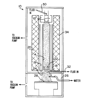
schematic representation of FIG. 1, which shows an arc jet
apparatus 10. The apparatus 10 includes a cathode member 12 at the
top end of a hollow barrel 14 in a metal jacket member 18 having an
annular space 19 suitable for holding a fluid coolant. The barrel
14 and jacket member 18 are surrounded by a fluid-cooled magnetic
coil assembly 20. Longitudinally spaced at the end of the barrel
14 opposite that of the cathode 12 is an anode member 22 having a
central opening aligned with the axis of the barrel 14 and leading
through a nozzle 24 into an evacuated deposition chamber 26 which
has a cooled deposition substrate 28 spaced from the end of the
nozzle 24. A gas injection means 30 is located to inject gas into
the barrel 14. Other gas injection means 32 are located in the
vicinity of the anode 22.
In the operation of the arc jet apparatus 10, hydrogen gas is
injected through the injector tubes 30 and 32 at a predetermined
rate. More hydrogen gas, mixed with methane, is injected through
the tube 32. The concentration of methane is based on the total
percentage of methane injected as a volume percent of the total gas
injected through both tubes 30,32. A direct current arc is struck
between the cathode 12 and anode 22. The enthalpy of the gas in
the barrel is adjusted by control of the arc power to result in the
5
CA 02281972 1999-09-16
IF-2934
desired temperature of the substrate 28, which is heated by the gas
impinging from the nozzle 24. At this enthalpy, the hydrogen
becomes partially dissociated hydrogen atoms. The magnetic coil
assembly 20 around the barrel 14 generates a solenoidal magnetic
field which has the effect of swirling the arc about the anode 22
to reduce anode erosion.
The activated gas mixture traveling through the nozzle 24
enters the evacuated deposition chamber 26 and impinges on a fluid-
cooled deposition substrate 28 therein to form a diamond film on
it. As the methane enters the activated gas through the tubes
32, it too becomes partially dissociated into unstable hydrocarbon
radical species. A set of three aluminum oxide ceramic tubules 34
positioned in radial symmetry with their ends in the deposition
zone between the nozzle 24 and the substrate 28 are fed with water
by a peristaltic pump, not shown. At the substrate 28, the
hydrogen acts as a facilitating gas for the deposition of the
carbon atoms from the activated hydrocarbon radicals as diamond
crystallites bonded to each other. The diamond crystallites
consist of carbon atoms bonded chemically to each other by what is
generally referred to as "spa" bonds.
Apparatus of the arc jet type, such as the apparatus 10
described above, is known in the art, except for the water
injection apparatus including the tubules 34. There are, of course
variations is such apparatus and in the methods of operating it.
Therefore, many other parameters are involved in the deposition
process. However, it is submitted that the most important ones are
generally the enthalpy (kilojoules/gram), vacuum level (torr),
6
CA 02281972 1999-09-16
LF-29'34
substrate temperature (degrees Celsius), methane concentration
(percent), and water injection rate. Given these parameter values,
the others can be determined for a given apparatus design and
method of operation by the skilled operators familiar therewith
without the necessity of undue experimentation. Such parameters do
not lend themselves well. to generalization, since they are
dependent on specific apparatus design features.
The gases used must be highly pure with respect to certain
elements. There should be an impurity level of less than 1,000 ppm
(parts per million) for substances other than hydrogen, carbon,
oxygen, argon, and helium. If the objective is to grow a free-
standing diamond film, the deposition substrate is preferably
molybdenum which has been coated with a thin layer about 3 microns
(micro-meters) thick of titanium nitride, such as by vapor
deposition, to reduce the adherence of the diamond to the substrate
for better release of the film.
Diamond film samples were made on an apparatus essentially
similar to the jet apparatus 10 described above. In each case, the
arc power was between 20 and 40 kilowatts and the deposition rate
was between 3 and 6 microns per hour. The temperature of the
substrate is in degrees C (Celsius).
7
CA 02281972 1999-09-16
IF-2934
deposition conditions
Sample A B C D E F
chamber press. (torr) 12 12 12 12 12 12
substrate temp. (C) 825 844 825 933 850 840
% methane .050 .052 .076 .050 .072 .050
enthalpy (kJ/g) 32.9 31.8 35.4 34.5 50.4 35.3
power in kW 29.6 28.6 31.8 31.2 31.6 31.8
water in g/min. 0 0 0 0 2 2
O/C molar ratio 0 0 0 0 7 7
thickness (microns) 308 400 383 357 410 300
analysis of deposited samples
Sample A B C D E F
Raman FWHM (/cm) - 2.8 4.6 6.5 - 2.9
thermal cond. (W/mK) 1130 - 1230 1110 1430 1430
collection distance 3 4 3 2 45 41
(microns)
lattice constant - - 3.568 3.567 3.566 3.570 3.569
(Angstroms)
The substrate temperature is in degrees Celsius as measured by
a pyrometer. The percent methane is the proportion by volume of
the methane in the gas added through the tubes 30,32. The enthalpy
is in kilojoules per gram. The power is the arc power in
kilowatts. The water injection rate is in grams per minute. The
O/C molar ratio is the molar ratio of oxygen to carbon in the
deposition zone between the nozzle 24 and the substrate 28. The
8
CA 02281972 1999-09-16
IF 2934
thickness is that of the diamond being deposited on the substrate
28. The Raman FWHM is in units of reciprocal centimeters and is
the full width at half the maximum of the Raman scattering 1332/cm
peak which is characteristic of diamond. The thermal conductivity
was measured by the converging wave method. Such a method is
described, for example, in_"Measurement of thermal diffusivity of
Polycrystalline Diamond Film by the Converging Thermal Wave
Technique," by G. Lu and W.T. Swann in Appl. Phys. Letters 59 (13),
Sept. 23, 1991. It is generally recognized that there can be
substantial variations in thermal conductivity measurements from
method to method. The collection distance was measured by a
particle-induced conductivity technique of the type described in
"Particle-And Photo-Induced Conductivity In Type IIA Diamonds" by
L.S. Pan et al, Journal of Applied Physics, July 15, 1993. The
samples were not subjected to a radiation annealing process of the
type sometimes referred to as "pumping" or "priming," which would
significantly increase the collection distance. It is a drawback
of the annealing process, however, that it tends to result in
drifting of the baseline and is therefore troublesome in practical
use. It is believed that the local collection distance of a given
quality material is directly proportional to the distance from the
surface of the diamond which was in contact with the substrate
during deposition. We have therefore normalized all collection
distances to a thickness of 400 microns. The lattice constants
were measured by standard x-ray diffraction means. Polishing of
the surface of the diamond which was in contact with the substrate
during deposition can also produce an increase in the collection
9
CA 02281972 1999-09-16
I~ 2934
distance, but is a costly and difficult process because of the
fragility and hardness of such thin diamond. It is an advantage of
the diamond material in accordance with the present invention that
it has a collection distance long enough to permit its use in a
particle detector device without annealing or polishing.
MATERIAL
The results shown in the above table permit some observations
with regard to characteristics of diamond material with a long
collection distance. It is noted, for example, that Raman line
width appears to be narrower for materials with increased
collection distance. Also, there appears to be a correlation
between a larger lattice constant and the collection distance, with
a lattice constant of 3.569 or greater representing a dramatic
increase in the collection distance. The thermal conductivity also
appears to be improved for the samples E and F with the long
collection distance.
The collection distances were measured with an electric field
strength of 10 kilovolts per centimeter. In order for the diamond
material to have a long carrier collection distance, it is
essential that it be substantially free from most crystal lattice
defects. Since the defects are microscopic, it is useful to assess
their concentration by measuring certain characteristics of diamond
which have been found to provide some indication of the degree to
which defects are present. These characteristics are Raman line
width and the thermal conductivity.
The results show that the specimens made with the added
CA 02281972 1999-09-16
LF 2934
oxidant exhibit a much longer collection distance. Experience
would also lead to a conclusion that samples E and F made with
injected water are likely to contain less than 100 ppm (parts per
million) of conductivity-enhancing impurities.
The Raman linewidth is the full line-width at half the maximum
of the 1332/cm frequency Raman scattering spectrum line of diamond.
This width gives an indication of the degree of ordering of the
diamond. The analysis of the samples A-F show that diamond with
larger Raman line widths has much reduced collection distances.
The examples show that a narrow Raman line profile, while perhaps
not alone a sufficient condition for determining that a material
will exhibit a long collection distance, does appear to be
associated with material having a long collection distance.
We have also noted that only samples with relatively high
levels of thermal conductivity exhibit long collection distances,
although high thermal conductivity does not by itself guarantee
long collection distance.
While it has been previously suggested by others in the art
that the addition of oxygen, such in the form of water, to a
combustion, thermionic, or microwave CVD diamond manufacturing
process would have a favorable effect on the quality of the
resulting diamond material, the discovery of the present invention
that the addition of oxygen, such as with water, to an arc jet
process with very low methane would result in a material with a
substantially improved charge carrier lifetime was not known
before.
The diamond material in accordance with the present invention
11
CA 02281972 1999-09-16
B~ 2934
typically has a collection distance of 35-50 microns. The mobility
is 3000-4000 cmz V1 s'1 and the lifetime is over 1 ns. This
increased lifetime is much higher than that previously reported as
best in the literature for CVD diamond (150 ps) and is even higher
than for natural IIa diamond (300-550 ps). The addition of water
is seen to greatly improve the lifetime. Under identical
conditions except for water, the diamond made without water had a
lifetime of 120 ps while the diamond made with water had a lifetime
of over 1 ns. Both had mobilities of 3000-4000 cm2 V-1 s-'.
The collection distance is measured by applying a voltage to
the electrodes on each side of the diamond and analyzing the signal
after it has been amplified by a charge-sensitive preamplifier and
by a signal shaping amplifier. The initial particles to be
detected can be from a radioactive source (e.g. strontium 90) or
from a particle accelerator beam line. The collection distance is
determined from
d- Qmeas t
Qgen
where "Qg~" is the amount of charge generated by the ionizing
radiation. "Q,~~" is the measured charge and "t" is the diamond
thickness. "Qg~" is calculated by normalizing the diamond pulse
height to the silicon pulse height (with corrections) or using a
Monte Carlo simulation.
The mobility and lifetime are measured by W transient
photoconductivity. One mm wide electrodes are deposited on the
same side of the diamond with a 1 mm gap between the electrodes.
12
CA 02281972 1999-09-16
IF-2934
The gap is illuminated with 3 to 5 ps (picosecond) pulses from a
202 nm frequency-multiplied Nd-YAG (neodymium-yttrium aluminum
garnet) laser. These pulses are typically up to 20 ~,J/pulse at 10
Hz. The UV pulse creates electron-hole pairs and the subsequent
current pulse is related to the carrier lifetime while the
amplitude and total charge. are related to the product of mobility
and lifetime. In this test, only the top 2 microns at the surface
is sampled due to the intrinsic absorption of W light by diamond.
In the particle-induced conductivity tests, the performance of the
entire diamond thickness is sampled. Since the material on the
substrate side is poorer and has small grain size, the particle-
induced conductivity test gives a collection distance which is
smaller than that deduced from the photoconductivity tests. The
difference is typically a factor of two.
DEVICE
FIGURE 2 of the drawings shows a particle detector 36 which
features a wafer 38 of CVD diamond according to the present
invention provided with two ohmic contact metal electrodes 40, 42 on
its faces. The electrodes 40,42 are connected to signal processing
circuitry which includes a voltage source in series with a load
resistor 46. An amplifier 48 is connected to the electrode 40 via
an isolation capacitor 50. Electrodes could alternatively be in
the form of interleaved comb-like structures which are both on the
same face of the wafer. Such device structures are presently known
in the art for use with diamond other than that of the present
invention. The operation of the device is as described earlier in
13
CA 02281972 1999-09-16
DF=2934
the discussion of such detector devices.
GENERAL CONSIDERATIONS
There is reason to assume that other oxidants, such as carbon
dioxide, can be used in place of water for providing the oxidant
used in the process. In addition, acetone, acetylene, and alcohols
have been reported as substitutes for methane as the carbon source
gas which would also contribute oxygen to the mix. These are
expected to give similar results to methane with water if the
concentrations are adjusted appropriately: generally each atom of
oxygen bonds firmly to one carbon atom, so that a molecule such as
acetone (CH3COCH3) contributes about as much free carbonaceous
species as two molecules of methane (CH4). The term "oxidant"
herein is used to denote substances traditionally considered in
this class in the chemical arts. Tightly bonded molecules such as
acetylene are less effective in producing diamond than are
molecules like methane. However, if the residence time of the
acetylene molecule is long enough, it may convert partially to more
active species such as methane in flight. If the acetylene (or any
other molecule) is injected into the arc, then it is substantially
broken up and should count as if the carbon were present as methane
(unless oxygen is present). Thus, it would be expected that one
could obtain results similar to those described above in accordance
with the invention by the use of carbon source gas other than
methane which includes one or more oxygen atoms and is present in
a concentration equivalent to that of the methane concentration
disclosed herein in terms of the resulting active species. Sulfur
14
CA 02281972 1999-09-16
LF 2934
and the halogens fluorine and chlorine could also be expected to
improve the collection distance by oxidizing impurities and
attacking structural defects much as oxygen appears to do in the
deposition process. Therefore, the invention is not intended to be
limited tv the use of methane alone as the carbon source gas or
water alone as the oxidant source. However, water is a
particularly advantageous oxidant source from the standpoint of
convenience, cost, and safety considerations.
Similarly, while here the facilitating gas is hydrogen, it has
been shown by those skilled in the art that there may be other
gases used to facilitate the growth of diamond films.