Note: Descriptions are shown in the official language in which they were submitted.
CA 02282166 1999-09-10
METHOD AND APPARATUS FOR BRIDGING A DIGITAL SIGNAL PROCESSOR
TO A PCI BUS
Field of the Invention
This invention relates to the field of bus bridging systems and more
particularly to
a method and apparatus for bridging one or multiple digital signal processors
with
a peripheral component interconnect bus.
Background of the Invention
The use of a Peripheral Component Interconnect (PCI) bus in the embedded
systems market is increasing at a rapid pace. PCI originated in the personal
computer (PC) industry where it was developed to relieve the input/output
(I/O)
bottleneck in graphics-oriented personal computer interfaces. However, despite
its origins in the PC market, PCI is expanding into industrial and embedded
systems applications and has emerged as the de facto local bus standard. This
is
primarily due to the motivation of designers of high performance embedded
systems to leverage component volumes from the PC industry to lower the cost
of
their products. Large segments of the embedded systems market are rapidly
standardizing on PCI, but are facing technical challenges in adapting their
processing platforms to PCI architecture.
The ability of digital signal processors (DSPs) to perform high-speed
arithmetic,
input/output (I/O) and interrupt processing operations has made them popular
in
communications applications. Currently, DSPs are used in a broad range of
embedded consumer and industrial communications products (e.g. cellular
phones, modems, call processing systems, wireless base stations, video
conferencing systems, routers, etc.). Multiprocessor configurations are also
widespread, particularly in communications servers that must support diverse
functions and a large number of channels.
CA 02282166 1999-09-10
2
The current challenge is to bridge these two merging technologies and provide
full
function PCI interface solutions for DSPs. In general, a DSP includes a host
port
interface (HPI) and an external memory interface (EMIF). The HPI is generally
a
16 bit slave and the EMIF is generally a 32 bit master (e.g. for the Texas
Instruments C6201TM DSP). Traditional solutions involve interfacing directly
with
the HPI of the DSP. Further, traditional bridging solutions do not provide
support
for multiple DSPs interfacing with a PCI bus.
Summary of the Invention
An object of the present invention is to provide a system for bridging a
digital
signal processor to a PCI bus.
Another object of the present invention is to provide a system for bridging
multiple
digital signal processors to a PCI bus.
In accordance with one aspect of the present invention there is provided an
apparatus for bridging communications between a first communication endpoint
equipped with a two port digital signal processor (DSP) circuit having a DSP
master port and a DSP slave port and a second communication endpoint
equipped with a peripheral component interconnect (PCI) bus module having a
PCI master port and a PCI memory connected to a PCI bus. The apparatus being
comprised of an intermediate bus operably connected to the DSP master port and
the DSP slave port and a regulating means connecting the PCI bus module to the
intermediate bus for regulating access to the intermediate bus and data
transfer
between the first and second communication endpoints.
In accordance with another aspect of the present invention there is provided a
method of carrying out a read transaction over a communications bridge between
one communication endpoint equipped with a digital signal processor (DSP)
circuit having a DSP master port and a DSP slave port and another
CA 02282166 1999-09-10
3
communication endpoint equipped with a peripheral component interconnect
(PCI) module having a PCI master port and a PCI slave port, an intermediate
bus
being operably connected to the DSP master port, the DSP slave port, the PCI
master port, and the PCI slave port. The read method consists of regulating
access to the intermediate bus for data transfer between a requesting master
port
and a requested slave port and transacting data for reading by the requesting
master port from the requested slave port.
In accordance with another aspect of the present invention there is provided a
method of carrying out a write transaction over a communications bridge
between
one communication endpoint equipped with a digital signal processor (DSP)
circuit having a DSP master port and a DSP slave port and another
communication endpoint equipped with a peripheral component interconnect
(PCI) module having a PCI master port and a PCI slave port, an intermediate
bus
being operably connected to the DSP master port, the DSP slave port, the PCI
master port, and the PCI slave port. The write method consists of regulating
access to the intermediate bus for data transfer between a requesting master
port
and a requested slave port and transacting data for reading by the requesting
master port from the requested slave port.
Brief Description of the Drawings
The present invention will be described in conjunction with the drawings in
which:
Fig. 1 illustrates a block diagram of a bridging system for a single digital
signal processor according to an embodiment of the present invention;
Fig. 2 illustrates a block diagram of a bridging system for multiple digital
single processors according to another embodiment of the present invention;
Fig. 3A illustrates a block diagram of the bridge module shown in Figs. 1
and 2;
Fig. 3B illustrates block diagrams of the I-BUS slave channel, the IDMA
channel and the PCI bus target channel shown in Fig. 3A;
CA 02282166 1999-09-10
4
Fig. 4A illustrates a block diagram of the control module shown in Figs. 1
and 2 according to an embodiment of the present invention;
Fig. 4B illustrates a block diagram of the control module shown in Figs. 1
and 2 according to another embodiment of the present invention;
Fig. 5 illustrates a timing diagram of various signals used to arbitrate
multiple DSPs access to the I-BUS shown in Fig. 2;
Figs. 6A-6B illustrate a flow chart of a PCI-HPI read transaction according
to the present invention;
Figs. 7A-7B illustrate a flow chart of a PCI-HPI write transaction according
to the present invention;
Fig. 8 illustrates a timing diagram of a bridge module read transaction
according to the present invention;
Fig. 9 illustrates a timing diagram of a bridge module write. transaction
according to the present invention;
Fig. 10 illustrates a timing diagram of a single PCI read transaction
according to the present invention;
Fig. 11 illustrates a timing diagram of a single PCI write transaction
according to the present invention;
Fig. 12 illustrates a timing diagram of a DMA write transaction according to
the present invention;
Fig. 13 illustrates a timing diagram of a DMA read transaction according to
the present invention;
Fig. 14 illustrates a timing diagram of an SRAM read transaction according
to the present invention;
Fig. 15 illustrates a timing diagram of an SRAM write transaction according
to the present invention;
Fig. 16 illustrates a timing diagram of an HPI read transaction according to
the present invention;
Fig. 17 illustrates a timing diagram of an HPI write transaction according to
the present invention;
CA 02282166 1999-09-10
Fig. 18 illustrates a timing diagram of an SRAM read transaction according
to the present invention; and
Fig. 19 illustrates a timing diagram of an SRAM write transaction according
to the present invention.
5
Detailed Description of Embodiments of the Invention
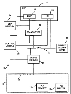
Fig. 1 illustrates a system block diagram of a bridge system 10 of the present
invention bridging a PCI bus module 17 to a digital signal processor (DSP) 14
using an intermediate bus (I-BUS) 16. The DSP 14 includes an external memory
interface (EMIF) 18 and a host port interface (HPI) 20. The EMIF 18 is
connected to a transceiver 22 and to a DSP memory 24. The system 10 includes
a bridge module 26, that communicates with the I-BUS 16 and a control module
28 that provides the necessary control and interface functions by polling the
EMIF
18, the HPI 20 and the transceiver 22. A shared memory (SRAM) 30 is provided
on the I-BUS 16. The PCI bus module 17 includes a PCI bus 12 to which a PCI
master port 13 and a PCI memory 15 are connected. The PCI master port 13 and
the PCI memory 15 collectively represent any device that communicates directly
with the PCI bus 12. Examples of PCI master devices 13 are a host processor
bus bridge, a network interface card, and other DSP bus bridges.
Fig. 2 illustrates a system block diagram of a multiprocessor bridge system 11
according to the present invention. In the system 11, multiple DSPs 14 are
connected to the I-BUS 16 and are simultaneously bridged to the PCI bus module
17. The connection topography of each DSP 14 to the I-BUS 16 and the control
module 28 are individually identical to that shown in Fig. 1. The connections
between the control module 26 and the DSP ports 18 and 20 have been removed
for simplicity.
CA 02282166 1999-09-10
6
~-BUS
The I-BUS 16 is a native processor bus to the bridge module 26. Each I-BUS 16
transaction involves a master and a slave. The bridge system 10/11 transforms
the DSP's HPI 20 and the shared memory 30 into I-BUS slaves, and allows the
DSP's EMIF 18 to become an I-BUS master so it can access the shared memory
30 and the PCI bus 12 for DSP 14 initiated transactions. For PCI bus module 17
initiated transactions the bridge module 26 becomes the I-BUS master,
described
in detail below.
The I-BUS 16 facilitates interprocessor communication in the case where
multiple
DSPs 14 are found (see Fig. 2) by allowing multiple DSPs 14 to communicate
over the I-BUS 16. Additionally, the I-BUS 16 provides access to DSP shared
memory 30 as described below.
With the use of the I-BUS 16 to connect to external devices each DSP 14 can
run
independently until I-BUS 16 access is required. This reduces the dependency
on one bus; a problem in direct interfacing. For all DSP 14 initiated
transactions
local buses may be used, but for all interprocessor and externally initiated
transactions it is necessary to use the I-BUS 16
SRAM
The control module 28 facilitates inter-processor communication by providing
support for the SRAM 30 on the I-BUS 16. Through arbitration, address mapping
and the generation of control signals, the control module 28 allows access to
the
SRAM 30 by all DSP(s) 14. The SRAM 30 acts as a communication mechanism
between all DSPs 14 (wherein access to the SRAM 30 is through the I-BUS 16)
by providing a storage location for shared data structures and for message
passing. The SRAM 30 is also used as a storage location for information
CA 02282166 1999-09-10
7
requested by the PCI bus module 17. The SRAM 30 is a typical asynchronous
memory resource well known to those skilled in the art.
PCI Bus Module
The PCI bus module 17 is collectively the PCI bus 12 and all devices attached
to
the PCI bus 12. For description simplification purposes the PCI memory 15 can
be viewed as a target (or slave) port of the PCI bus module 17. The PCI master
port 13 and the PCI memory 15 are often part of the same device connected to
the PCI bus 12.
The PCI bus 12 acts as a foundation for the MicrosoftTM/IntelTM Plug and Play
(PnP) PC architecture. Through the use of configuration registers within any
PCI
resource, the operating system can reallocate system memory and allow a PC to
be dynamically reconfigured. Resource configuration space is divided into
three
areas: (1) a device-independent header region; (2) a header-type region; and
(3)
a user-defined region. Further information regarding the PCI architecture can
be
found in standard PCI bus specifications known to those skilled in the art.
Transceiver
The transceiver 22 acts as an isolator between the I-BUS 16 and the DSP 14.
This keeps the electrical activity of the I-BUS 16 isolated from the activity
of the
EMIF 18. In the case where multiple DSPs 14 access the I-BUS 16, the activity
over the I-BUS 16 may not be concerned with all connected DSPs 14. With an
open connection between the DSPs 14 and the I-BUS 16 there would invariably
be noise received by each DSP 14 due to transactions from other DSPs 14 taking
place over the I-BUS 16.
CA 02282166 1999-09-10
As there is no need to isolate the control module 28 from the EMIF 18, a
direct
link between these two components exists. This connection allows separate
requests to be made by the EMIF 18 to the control module 28 without the
intervention of the transceiver 22. The control module 28 and transceiver 22
are
connected to allow the control module 28 to open a connection between the EMIF
18 and the 1-BUS 16. This allows the EMIF 18 to send a request to the control
module 28 to open a connection between the EMIF 18 and the I-BUS 16.
Through signals given by the control module 28, the transceiver 22 controls
data
flow and the direction of the data flow.
DSP Memory
Each DSP 14 may possess its own DSP memory 24 that may be accessed only
by that DSP 14 as in Fig. 1. Alternatively, multiple DSPs 14 can share a
single
DSP memory 24 as in Fig.2. The DSP memory 24 contains information
necessary for booting the DSP 14 via the PCI bus module 17. This DSP memory
24 offers performance advantages for its associated DSP 14 that are beyond
what is possible in the SRAM 30.
EMIF DSP
The EMIF port 18 is the DSP's 14 general purpose external memory interface.
The EMIF 18 is the master of the DSP 14 and as such initiates all DSP circuit
14
initiated transactions. The EMIF 18 allows for signal I/O under direct memory
access (DMA) while processing continues uninterrupted in the foreground. It
may
also be used for external I/O functions.
CA 02282166 1999-09-10
9
HPI DSP
The HPI port 20 is a general-purpose I/O port that may be used by another
transaction initiating device to access the DSP 14. The HPI 20 is the slave of
the
DSP14 . Data presented at the HPI port 20 is automatically written into
internal
DSP memory (not shown) without stopping the DSP 14, allowing simultaneous
transmission and receipt:
Bridge Module
Fig. 3A provides a detailed block diagram representation of the bridge module
26.
The bridge module 26 includes two interfaces: a PCI interface 40 and an I-BUS
interface 46. The bridge module 26 acts as the gateway between the PCI bus
module 17 and the I-BUS 16 based on control signals from the control module
28.
The PCI interface 40 is the bridge module's 26 connection to the PCI bus
module
17 and includes a PCI master module 42 and a PCI target module 44.
The I-BUS interface 46 is an interface that connects the bridge module 26 to
the 1-
BUS 16 and includes an I-BUS slave module 48 and an I-BUS master module 50.
The two interfaces 40 and 46 are connected to different functional channels
operating in the bridge module 26. The channels include: an I-BUS slave
channel
52, an IDMA channel 54, a register channel 56, an interrupt channel 58 and a
PCI
bus target channel 60 discussed in further detail below.
PCI Master Module
The PCI master module 42 is a PCI standards compliant port with a 32 bit
multiplexed address/data bus. The PCI cycles of the bridge module 26 are
synchronous, meaning that bus and control input signals are externally
synchronized to a PCI clock. The PCI master module 42 is available to either
the
I-BUS slave channel 52 or the IDMA channel 54. The PCI master module 42 acts
as the master of the PCI bus module 17 when the PCI memory 15 is the slave
CA 02282166 1999-09-10
port of the current transaction making the current transaction a DSP 14
initiated
transaction.
PCI Target Module
5 The PCI target module 44 is a PCI compliant port with a 32 bit multiplexed
address/data bus. The PCI cycles are synchronous as discussed in relation to
the master module 42. The bridge module 26 requests PCI bus mastership from
the control module 28 through its PCI target module 44. The PCI target module
44 is the slave of the PCI bus module 17 when the master of the current
10 transaction is the PCI master 13 the current transaction a PCI bus module
17
initiated transaction.
I-BUS Slave Module
The I-BUS slave module 48 is a non-multiplexed 32 bit address, 32 bit data
interface. The I-BUS slave module 48 is capable of receiving and processing
requests from an I-BUS master module 50, described in detail below. The I-BUS
slave module 48 is the slave when the current transaction is a DSP 14
initiated
transaction and the 1-BUS master is the DSP EMIF 18.
I-BUS Master Module
The I-BUS master module 50 is a non-multiplexed 32 bit address, 32 bit data
interface. The I-BUS master module 50 is capable of initiating and completing
requests made to 1-BUS slave modules 48. The I-BUS master module 50 is
master of the I-BUS 16 for PCI bus module 17 initiated transactions.
I BUS Slave Channel
The DSP 14 can access the PCI bus module 17 through the bridge module 26 by
using the I-BUS slave channel 52 or the IDMA channel 54. The I-BUS slave
channel 52 is used in read/write transactions when the I-BUS master wants to
access the PCI memory 15 (the target or slave). That is, the I-BUS slave
channel
CA 02282166 1999-09-10
11
52 is used for DSP circuit 14 initiated transactions. The IDMA channel 54 is
used
for high speed data transfer when the I-BUS 16 accesses the PCI memory 15.
A slave image is defined as a set of parameters in the I-BUS slave channel 52
that control transfers from the I-BUS 16 to the PCI bus module 17. Similarly,
a
target image is provided in the PCI bus target channel 60. In an illustrative
embodiment, two slave images are provided in the I-BUS slave channel 52 to
enable quick access to different PCI addresses from the I-BUS 16. The two
slave
images can be completely independent from one another. For example, in one
configuration, a slave image 0 can be used to access a hard-drive using memory
in PCI memory 15 and a slave image 1 would be available to access a different
device with its own memory size.
PCI Bus Target Channel
The PCI master port 13 can access the I-BUS slave 48 through the bridge module
26 by using the PCI bus target channel 60. The operation of the PCI bus target
channel 60 is generally illustrated in the timing drawings described herein
below
involving a path of a transaction from the PCI bus 12 to the I-BUS 16 that
involves
the following main steps: (1) address phase, (2) data transfer, (3) I-BUS
arbitration, and (4) termination.
IDMA Channel
Direct memory access transactions are initiated on the I-BUS 16. The IDMA
channel 54 is used for high speed access of the PCI memory 15 by the EMIF 18.
The I-BUS slave module 48 accepts IDMA read and write transfers.
Register Channel
The register channel 56 is used to program PCI settings and to define
operating
parameters of the bridge module 26. Registers in the register channel 56 can
be
accessed from either the PCI bus module 17 or the I-BUS 16. Due to this dual
CA 02282166 1999-09-10
12
access support, an internal pointer selects which bus can access the
registers.
Default ownership of the register channel 56 is granted to the PCI tafget
module
44. When ownership of the register channel 56 is granted to the I-BUS slave
module 48, register accesses from the PCI bus module 17 are retried.
Interrupt Channel
The interrupt channel 58 is used to support certain hardware and software
events
that trigger interrupts on the I-BUS 16 and the PCI bus 12. A hardware
interrupt
involves a signal on one interface triggering an interrupt on an opposite
interface.
A software triggered interrupt is generated by the bridge module 26 based on
internal events.
Further detailed block diagrams of channel 52, 54 and 60 are shown in Fig. 3B.
The 1-BUS slave channel 52 includes a first-in-first-out write buffer 52a (Ix-
FIFO)
for posted writes; a first-in-first-out read buffer 52b (Ir-FIFO) for pre-
fetched reads;
and a delayed single transfer buffer 52c.
The IDMA channel 54 includes a first-in-first-out buffer 54a for posted writes
and
pre-fetched reads. The PCI bus target channel 60 includes a first-in-first-out
write
buffer 60a (Px-FIFO) for posted writes; a first-in-first-out read buffer 60b
(Pr-FIFO)
for pre-fetched reads; and a delayed single transfer buffer 60c.
The delayed single transfer buffers 52c/60c are used for storing a single data
entry and an associated address entry. These delayed single transfer buffers
52c/60c are used to improve write performance and read performance of
transactions between the PCI bus module 17 and the I-BUS 16.
CA 02282166 1999-09-10
13
Control Module
Figs. 4A and 4B provide detailed. block diagram representations of two
embodiments of the control module 28/28' respectively (collectively referenced
by
numeral 28). The control module 28 coordinates signaling and arbitration of
the
bridge module 26 and the DSP 14 to provide PCI protocol translation. The
control
module 28 includes an I-BUS control section 80, a DSP control section 82 and
an
arbitration section 84. The DSP control section 82 includes an HPI controller
90
and an EMIF controller 92 (in the embodiment of Fig. 4A). The arbitration
section
84 includes an I-BUS arbiter 94 and a DSP arbiter 96.
I-BUS Control Section
The I-BUS control section 80 includes an address decoder 86 and a controller
88.
The selection of I-BUS slaves in the bridge module 26 is memory mapped in the
address decoder 86. The address decoder 86 provides the memory mapping that
controls the generation of required chip select signals. The address decoder
86
determines which device on the I-BUS 16 is to be selected for the current
transaction. It does so by decoding the address lines of the I-BUS 16.
If an address is decoded as a register access, the control module 28 asserts,
through the I-BUS control section 80, a register chip select signal (CSREG).
If an
address is decoded as an EMIF-PCI access, the control module 28 asserts,
through the I-BUS control section 80, a PCI chip-select signal (CSPCI) and one
of
two bridge slave images of the channel in use is selected. The bridge slave
images can be those of the I-BUS slave channel 52, the register channel 56 or
the
IDMA channel 54.
The control module 28 asserts an image select signal (IMSEL) to determine
which
of the two bridge slave images is used. If the IMSEL signal is at a logic 0, I-
BUS
slave image 0 is selected. If the IMSEL signal is at a logic 1, I-BUS slave
image 1
is selected.
CA 02282166 1999-09-10
14
If an address is decoded as a direct memory access (IDMA) and the bridge
module 26 asserts an IDMA request signal (DREQ) then the control module 28
asserts an IDMA acknowledge signal (DACK). If an address is decoded as an
SRAM access from either the bridge module 26 or the DSP 14 then the control
module 28 asserts an SRAM chip select signal (CS).
If an address is decoded as a PCI-HPI register access, then the control module
28 asserts an HPI chip select for DSP signal (HCS) and an HPI control signal
(HCNTL) to determine which DSP's 14 host port register 20 will be accessed.
Details of the signals referenced above are provided in Table A1 at the end of
the
disclosure portion of the application.
The controller 88 is involved in a series of the different transaction types
on the I-
BUS 16. A sample list of I-BUS 16 transactions is provided in Table B1.
TABLE B1
MASTER TARGET TRANSACTION 1-BUS
TYPE PROTOCOL
DSP 14 Bridge module Bridge module I-BUS master
26 Register access
DSP 14 Bridge module EMIF PCI access I-BUS master
26
DSP 14 Bridge module IDMA access IDMA master
26
DSP 14 Shared memory Shared memory DSP 14 memory
(SRAM) 30 access
Bridge module SRAM 30 Shared memory Bridge module
26 access 26
memory
Bridge module HPI 20 of DSP PCI HPI access I-BUS slave
26 14
CA 02282166 1999-09-10
One of the general tasks the controller 88 performs is handshaking on the I-
BUS
16 for both DSP(s) 14 and bridge module 26 transactions. In the I-BUS slave
mode, the controller 88 terminates bridge module 26 master channel
transactions
5 targeted at the DSP's HPI 20 or the shared memory 30. In master mode, the
controller 88 generates arbitration and control signals on behalf of the DSP's
EMIF 18 for accessing the bridge module 26. For the shared memory 30 access,
the controller 88 also generates SRAM cycles for both the DSP(s) 14 and the
bridge module 26.
As detailed in Table B1 above, the control module 28 supports flue different
protocols on the I-BUS 16 for reads and writes: I-BUS master, I-BUS slave,
IDMA
master, DSP(s) memory, and bridge module memory.
I-BUS mastering supports the following DSP(s) 14 transactions: bridge module
26
register access and PCI access via the I-BUS slave channel 52 of the bridge
module 26 (i.e. EMIF-PCI access). Two conditions qualify a transaction as an I-
BUS master cycle. First, the I-BUS arbiter 94 grants the DSP(s) 14 the I-BUS
16.
Second, the DSP(s) 14 is engaged into an I-BUS access cycle involving the
register channel 56 of the bridge module 26 as decoded by the address decoder
86. With these two stipulations met, the DSP 14 can then perform read or
writes
to either the register channel 56 of the bridge module 26 or the PCI bus
module
17.
The I-BUS slave protocol of the control module 28 supports access by the
bridge
module 26 to the HPI 20 of the DSP 14. An I-BUS slave cycle occurs once the
bridge module 26 is granted the I-BUS 16 by the I-BUS arbiter 94 and the I-BUS
16 is engaged into a HPI I-BUS access cycle as indicated by the address
decoder
86. The bridge module 26 then asserts a bus busy (BB) signal and the
controller
88 engages the HPI controller 90.
CA 02282166 1999-09-10
16
For each slave cycle, the control module 28 provides a termination code
depending on the state of the HPI transaction returned by the HPI controller
90,
and the HPI 20 sources or sinks data if ready. If the termination code is
RETRY
then the bridge module 26 will cause the entire sequence to repeat otherwise
the
controller 88 will return to an IDLE state.
IDMA mastering supports high speed transfers with the DSP(s) 14 utilizing the
IDMA channel 54 of the bridge module 26. Two conditions qualify a transaction
as an 1-BUS master cycle. First, the DSP(s) 14 is granted the I-BUS 16 by the
I-
BUS arbiter 94. Second, the DSP(s) 14 is engaged into an IDMA access cycle as
indicated by the address decoder 86. Once these two qualifications are met,
the
control module 28 asserts control signals to initiate bridge module 26 IDMA
access. The bridge module 26 will sink or source data and send a termination
to
the EMIF controller 92 for processing.
The DSP(s) 14 shared memory access is aligned, for example to 32 bits wide,
read/write access to the shared memory 30. The control module 28 provides the
required shared memory control signals: chip select (CS), read strobe (RD),
and
write strobe (WR). In order for a DSP(s) 14 memory cycle to occur, the DSP(s)
14
must be granted the I-BUS 16 by the 1-BUS arbiter 94 and must also become
engaged into an I-BUS access cycle involving the shared memory 30 as decoded
by the address decoder 86. During DSP 14 shared memory access cycles, the
control module 28 polls the RD or WR signal based on signals sampled by the
EMIF controller 92.
The bridge module 26 shared memory access is aligned, for example to 32 bits
wide, read/write access to the shared memory 30. Two conditions qualify a
transaction as an I-BUS master cycle. First, the bridge module 26 must be
granted the I-BUS 16 by the I-BUS arbiter 94. Second, the I-BUS access cycle
CA 02282166 1999-09-10
17
must involve the shared memory 30 as decoded by the address decoder 86. For
these transactions, the control module 28 provides the CS and RDIWR strobes as
discussed above.
DSP Control Section
The DSP control section 82 includes an HPI controller 90 and an EMIF
controller
92. The control module 28' (of Fig. 4B) also includes an SRAM controller 93
according to an alternative embodiment of the present invention. The host port
interface 20 of the DSP 14 is a parallel port through which the PCI master
port 13
can access registers of the HPI 20. This type of transaction is termed a PCI-
HPI
access. The data path for PCI-HPI access includes the PCI bus target channel
60 of the bridge module 26. The PCI bus target channel 60 provides two
programmable target images at the PCI interface 40. Either target image can be
mapped to access the HPI 20 of the DSP 14 and both can execute delayed or
posted transactions.
The HPI controller 90 of the DSP control section 82 facilitates PCI-HPI access
by
interpreting the transaction signals from the bridge module 26 and controlling
the
transaction signals on the HPI 20. The HPI controller 90 asserts HPI chip
select
(HCS) and HPI control select (HCNTL) signals to direct a transaction to one of
three registers in the HPI 20 of the DSP 14: (1) HPI address register (HPIA),
(2)
HPI data register (HPID), and (3) HPI control register (HPIC).
The HPI controller 90 drives an HPI data strobe (HDS) and an HPI readlwrite
select (HR_llln signal to initiate the transaction on the HPI 20. The HPI
controller
90 also controls the transfer of data based on an HPI ready (HRDY) signal. If
the
HPI controller 90 samples the HRDY signal high, no data can be transferred.
The
control module 28 will generate retries on the I-BUS 16 until the HPI
controller 90
samples the HRDY signal low allowing the data transfer to proceed.
CA 02282166 1999-09-10
18
PCI-HPI accesses compliment multiprocessor system requirements such as the
system 11 shown in Fig. 2. The PCI master port 13 can access internal or I/O
memory of the DSP 14, as well as reading or writing to the registers (HPIA,
HPID,
and HPIC) of the HPI 20. Along with register access, the PCI master port 13
can
also interrupt the DSP 14 by writing to the HPIC register.
EMIF Controller
The external memory interface (EMIF) controller 92 supports DSP 14 access to
the I-BUS 16 allowing the DSP 14 to master the I-BUS 16. As an I-BUS master,
the EMIF 18 of the DSP 14 performs four different types of transactions: (1)
bridge register access; (2) EMIF-PCI access; (3) IDMA access; and (4) global
shared memory access to the shared memory 30.
The EMIF controller 92 manages transaction signals between the EMIF 18 of the
DSP 14 and the bridge module 26. This allows the DSP 14 to perform read/write
transactions on the PCI bus module 17 via the slave channel 52 of the bridge
module 26.
For IDMA access, the EMIF controller 92 works in conjunction with a DMA
controller (not shown) in the DSP 14 in order to manage transaction signals
for
transfers between the EMIF 18 of the DSP 14 and the IDMA channel 54 of the
bridge module 26.
To access the shared memory 30, the EMIF controller 92 manages the
transaction signals between the EMIF 18 of the DSP 14 and the memory 30
allowing the DSP 14 to read/write directly to the memory 30.
For all transactions initiated by the EMIF 18 of the DSP 14, the EMIF
controller 92
of the control module 28 interprets the transaction signals from the DSP 14
and
manages the transaction signals on the I-BUS 16. The DSP 14 indicates it is
CA 02282166 1999-09-10
19
ready to perform transactions by asserting a chip enable (CE) signal. The EMIF
controller 92 samples a byte enable (BE) signal and translates the signal into
an
I-BUS 16 byte enable signal. If the EMIF 18 initiates a read, the EMIF
controller
92 samples an asynchronous memory output enable (AOE) signal and an
asynchronous memory read (ARE) strobe.
If the EMIF 18 initiates a write, the EMIF controller 92 samples an
asynchronous
memory write (AWE) strobe. In both transactions, the EMIF controller 92 drives
a
asynchronous memory write (ARDY) strobe to regulate data flow. In particular,
the EMIF controller 92 asserts ARDY low to wait state the asynchronous
interface
and the transaction may resume once ARDY is asserted high.
As summarized in Table A1, ARDY is an active high asynchronous ready input
used to control data flow between the EMIF 18 and the I-BUS 16. The ARDY
signal commits the EMIF 18 until either a transaction completes or fails on
the I-
BUS 16. A detailed summary of ARDY behavior is provided in Table B2.
TARI F R7
TRANSACTION RETRY NORMAL ERROR
register read/writeARDY=0 ARDY=1 ARDY=1
(control module
28)
read/write ARDY=0 ARDY=1 ARDY=1
(EMIF 18-PCI 12) EINT=0
read/write DREQ=1 DREQ=0 ARDY=1
(IDMA) ARDY=0 ARDY=1 EINT=0
read/write NIA ARDY=1 NIA
(SRAM 30)
Interfacing with the EMIF allows for improved speed (bytes/second) as well as
a
reduction in latency (clocks/transaction completion).
CA 02282166 1999-09-10
SRAM Controller
As discussed above, the control module 28' of Fig. 4B includes the SRAM
controller 93. During DSP shared memory access cycles, the SRAM controller 93
5 strobes the RD or WR signal based on signals sampled by the EMIF controller
92.
The SRAM controller 93 facilitates access to the SRAM 30 by interpreting the
transaction signals from the bridge module 26 and controlling the signals on
the
SRAM 30. The SRAM controller 93 interfaces with the address decoder so that if
the SRAM 30 is the selected device the address decoder can notify the SRAM 30
10 through the SRAM controller 93.
Arbitration Section
The arbitration section 84 facilitates I-BUS 16 access arbitration for PCI
masters
as well as for the DSPs 14 in the multiple processor system 11 of Fig. 2.
15 Arbitration is a round-robin process for the DSPs 14 and provides priority
for
bridge module 26 accesses to the I-BUS 16. The arbitration section 84 points
to
the DSPs 14 to minimize EMIF 18 access latency.
When the DSP 14 initiates a transaction to the I-BUS 16 via the EMIF 18, the
20 EMIF 18 rnay not be used by the DSP 14 until that transaction is complete.
Therefore, in order to minimize EMIF 18 to I-BUS 16 access latency in a
multiple
DSP configuration (Fig. 2), it is the arbitration section 84 that must
efficiently grant
I-BUS 16 access. So the arbitration section 84 minimizes the amount of time
the
EMIF 18 waits for access to the I-BUS 16 as another transaction is taking
place.
The arbitration section 84 also controls the direction of data flow and
activity of
the transceivers 22 located between the EMIFs 18 of the DSPs 14 and the I-BUS
16.
CA 02282166 1999-09-10
21
UVhen a DSP read cycle is executed, the transceiver 22 drives the I-BUS 16
data
bus onto the EMIF 18 data bus. When the DSP 14 performs a write cycle, to the
I-BUS 16, the transceiver 22 drives data from the EMIF 18 to the I-BUS 16.
I-BUS Arbiter
All bridge module target channel accesses begin with the bridge module 26
requesting access to the I-BUS 16 from the control module 28. Both the control
module 28 and the bridge module 26 take part in I-BUS arbitration using a
three
wire handshake triggered by a clock signal, as illustrated in Fig. 5. The
bridge
module 26 begins by asserting a bus request (BR) signal. The control module 28
asserts a bus grant (BG) signal and negates a bus busy (BB) signal. When the
bridge module 26 samples BG asserted and BB negated, the bridge module 26
asserts BB and negates its BR. The BR, BG and BB signals are all synchronized
to the clock.
If the control module 28 asserts the bus busy signal in response to the bus
request signal from the bridge module 26, then the bridge module 26 wilt be
retried. The bus busy signal indicates that an active bus master is preparing
to
use or continuing to use the I-BUS 16. The current transaction will have to
complete before the bridge module 26 is granted access to the I-BUS 16 by the
control module 28. Upon being granted access to the I-BUS 16, the address
decoder 86 of the control module 28 decodes the I-BUS 16 address to determine
which DSP HPI 20 or SRAM 30 location is to be accessed.
DSP Arbiter
Each of the DSPs 14 (of system 11 in Fig. 2) interfaced to the control module
28
can request access to the I-BUS 16 via the DSP arbiter 96. The DSP arbiter 96
provides round-robin access to each of the DSPs 14. The requested DSP 14
asserts an I-BUS request (REQ) signal to the control module 28 to acquire
access
CA 02282166 1999-09-10
22
to the I-BUS 16. The I-BUS 16 is available when an I-BUS grant (GNT) signal is
asserted by the DSP 14.
Pending I-BUS 16 requests are re-evaluated at the following positive edge of
the
clock signal after the DSP 14 of the last granted request is released.
Interrupt Generation
There are two sources of interrupts to the DSP 14: (1) internal bridge module
26
interrupts and (2) I-BUS 16 errors. Interrupts generated by the bridge module
26
are available on a bridge module interrupt (INT) signal and can be enabled for
various internal and external events. The bridge module INT signal is reset
using
a bridge module ISR register on the receipt of each interrupt.
Errors encountered on the 1-BUS 16 are signaled by the control module 28. The
DSP 14 receives an I-BUS error interrupt (EINT) under one of the following
conditions: (1) the PCI bus 12 encounters delayed read or write results in
master
or target; (2) the bridge module 26 register access that generates PCI
configuration causing an abort; and (3) accessing a reserved location in a
memory map of the address decoder 86.
Transactions
A PCI-HPI read transaction 100 is illustrated in the flow chart of Figs. 6A-
6B. The
transaction 100 consists of the PCI master port 13 performing a PCI read from
an
HPI register in the HPI 20 of the DSP 14. The specific depiction of a PCI-HPI
read transaction 100 in Figs. 6A and 6B is exemplary and all read transactions
occur in a similar manner.
CA 02282166 1999-09-10
23
The PCI master port 13, having a specific address, asserts a read transaction
request on the PCI bus 12 at step 102. The bridge module 26 recognizes the
address of the PCI master port 13 and latches the address of the PCI master
port
13 at step 104.
The bridge module 26 requests the I-BUS 16 by asserting a bus request (BR)
signal at step 106. The control module 28 asserts a bus grant (BG) signal and
the
bridge module 26 asserts a bus busy (BB) signal at step 108 in response to the
bus request signal issued by the bridge module 26 at step 106.
The bridge module 26 then becomes an I-BUS master and initiates a read on the
I-BUS 16 at step 110. The bridge module 26 translates the address of the PCI
master port 13 into an I-BUS address using PC1 target image settings and
properties stored in the PCI target module 44 of the bridge module 26 at step
112.
The bridge module 26 asserts a read/write (RIIIn signal and a transaction
start
(TS) signal to the control module 28 at step 114.
The control module 28 determines, based on the I-BUS address determined at
step 112, which HPI 20 the request is for and asserts an HPI chip select (HCS)
signal, a register selector (HCNTRL) and a read request (HR_llln signal at
step
116.
The control module 28 asserts an HPI data strobe (HDS) at step 118 to indicate
to
the DSP 14 that there is an access/read request. If the DSP 14 does not have
the data ready to respond to the read request, the DSP 14 asserts the HPI
ready
(HRDI~ signal high to the control module 28 and the control module 28 in-turn
asserts a retry (TRETRI~ signal on the I-BUS 16 at step 120. The bridge module
26 then negates the bus busy (BB) signal at step 122.
CA 02282166 1999-09-10
24
The bridge module 26 and the control module 28 repeat steps 118-122 at step
124 until the HPI 20 of the DSP 14 has the data ready to answer the read
request. When the HPI 20 of the DSP 14 has the data available, the DSP 14
asserts the HPI ready (HRDY) signal low at step 126.
When the bridge module 26 asserts a transaction start (TS) signal, the DSP 14
drives the HPI data strobe and the data is read by the bridge module 26
directly
from the HPI 20 of the DSP 14 at step 128. After the data transfer, the
control
module 28 asserts a transaction acknowledge (TA) signal at step 130 to signal
to
the bridge module 26 the end of the cycle. Read cycles occur at step 132 as
long as the HRDY signal is low until the entirety of the read data is
transferred.
When the transaction is complete, the bridge module 26 negates the BB signal
to
terminate the transaction at step 134.
When the PCI master port 13 retries the same transaction - qualified by the
latched information-it is provided with the data from the bridge module 26 and
the
transaction terminates normally on the PCI bus 12.
A PCI-HPI write transaction 150 is illustrated in the flow charts of Figs. 7A-
7B.
The transaction 150 consists of the PCI master port 13 pertorming a PCI write
to
an HPI register in the HPI 20 of the DSP 14. The specific depiction of a PCI-
HPI
write transaction 150 in Figs. 7A and 7B is exemplary and all write
transactions
occur in a similar manner.
The PCI master port 13, having a specific address, asserts a write transaction
request on the PCI bus 12 at step 152. The bridge module 26 recognizes the
address of the PCI master port 13 and latches the address of the PCI master
port
13 at step 154.
CA 02282166 1999-09-10
The bridge module 26 requests the I-BUS 16 by asserting a bus request (BR)
signal at step 156. The control module 28 asserts a bus grant (BG) signal and
the
bridge module 26 asserts a bus busy (BB) signal at step 158.
5 The bridge module 26 then becomes an I-BUS master and initiates a write on
the
I-BUS 16 at step 160. The bridge module 26 translates the address of the PCI
master port 13 into an I-BUS address using PCI target image settings and
properties stored in the PCI target module 44 of the bridge module 26 at step
162.
The bridge module 26 asserts a read/write (RW) signal and a transaction start
10 (TS) signal to the control module 28 at step 164.
The control module 28 determines, based on the I-BUS address determined at
step 162, which HPI 20 the access is for and asserts an HPI chip select (HCS)
signal, a register selector (HCNTRL) and a write request signal (HR_W) signal
at
15 step 166.
The control module 28 asserts an HPI data strobe (HDS) at step 168 to indicate
to
the DSP 14 that is an access request. If the DSP 14 is not ready to accept the
write data, the DSP 14 asserts the HPI ready (HRDY) signal high to the control
20 module 28 and the control module 28 asserts a retry (TRETRY) signal on the
I-
BUS 16 at step 170. The bridge module 26 then negates the bus busy (BB)
signal at step 172.
The bridge module 26 and the control module 28 will repeat steps 168-172 at
step
25 174 until the HPI 20 of the DSP 14 is ready to accept the write data. When
the
HPI 20 of the DSP 14 is ready to accept the write data, the DSP 14 asserts the
HPI ready (HRDY) signal low at step 175.
When the bridge module 26 asserts a transaction start (TS) signal and the HRDY
signal is low, the bridge module 26 writes directly to the HPI 20 of the DSP
14 at
CA 02282166 1999-09-10
26
step 176. After the data transfer, the control module 28 asserts a transaction
acknowledge (TA) signal at step 178 to signal to the bridge module 26 the end
of
the cycle. Write cycles occur at step 180 as long as the HRDY signal is low
until
the entirety of the write data is transferred.
When the transaction is complete, the bridge module 26 negates the BB signal
to
terminate the transaction at step 182.
When the PCI master port 13 retries the same transaction - qualified by the
latched information-it is provided with termination signals and the
transaction
terminates normally on the PCI bus 12.
Timing
Details of read/write transactions between various components of the system
10/11 will be described in conjunction with the timing diagrams of Figs. 8 to
19.
A timing diagram for a read transaction of the bridge module 26 is shown in
Fig. 8.
During register reads the DSP(s) 14 begins by arbitrating for the
I-BUS 16 as discussed above. The address generated by the DSP 14 indicates
to the control module 28 that a register access is to be attempted. The
decoded
address causes the CSREQ signal to be asserted low.
The transceivers 22 are enabled and direction is determined by sampling the
state of the AOE signal at the next positive edge of clock signal when the CE
signal is detected low. The DSP 14 asserts the ARE strobe shortly after
asserting
AOE signal.
The control module 28 asserts the QA and SIZ signals to decode the BE signal
of
the DSP 14. The BE control signal may originate from the EMIF (going to the
CA 02282166 1999-09-10
27
control module 28) or from the control module 28 (going to the SRAM 30). The
action that the control module 28 takes on this signal depends on where it
originated. If the BE signal came from the EMIF 18 then the control module 28
will decode the signal to extract information for the SIZ and QA signals. If
the BE
signal is originating in the control module 28 then the control module 28 will
encode the BE signal with SIZ and QA information. The BE signal selects one of
4 bytes that are active on the DSP's EMIF interface 18. SIZ translates on the
I-
BUS 16 to a "port" size of 8/16/32 bits. QA translates to addressing of bytes
on
each of the possible port sizes.
The I-BUS 16 R/Vll signal is the inverse of the AOE signal for register
accesses.
The TS signal causes the bridge module 26 to produce a termination (TERM)
signal.
If the termination signal is normal then an ARDY signal is asserted and the
DSP
14 transaction will proceed. If the termination condition is an error then the
ARDY
signal is asserted along with an error interrupt (EINT) signal. If the
termination
condition is a retry then the control module 28 retries by asserting the TS
signal
until either a normal or error termination occurs.
A timing diagram for a write transaction of the bridge module 26 is shown in
Fig.
9. During register writes the DSP(s) 14 begin by arbitrating for the I-BUS 16
as
discussed above. The address generated by the DSP 14 indicates to the control
module 28 that a register access is to be attempted. The decoded address
causes the CSREG signal to be asserted low.
The transceivers 22 are enabled and direction is determined by sampling the
state of the AOE signal at the next positive edge of clock signal when the CE
signal is detected low. The DSP 14 asserts the AWE strobe shortly after
asserting AOE but can encounter wait states (i.e. ARDY signal low). The AOE is
CA 02282166 1999-09-10
28
asserted high throughout the entire clock cycle in Fig. 9 as a low signal
indicates
read and this is a write transaction.
The control module 28 asserts the QA and SIZ signals to decode the BE signal
of
the DSP 14. The I-BUS 16 R/W signal is the inverse of the AOE signal for
register accesses. The TS signal causes the bridge module 26 to produce a
termination (TERM) signal.
If the termination signal is normal then the ARDY signal is asserted and the
DSP
14 transaction is complete. If the termination condition is an error then the
ARDY
signal is asserted along with an error interrupt (EINT) signal. If the
termination
condition is a retry then the control module 28 will reassert the TS signal
until
either a normal or error termination occurs.
A timing diagram of a single PCI read transaction is shown in Fig. 10. During
single PCI reads the DSP(s) 14 begin by arbitrating for the I-BUS 16. The
address generated by the DSP 14 indicates to the control module 28 that a PCI
access is to be attempted. The decoded address causes the control module 28 to
assert the PCIREG and IMSEL signals.
The transceivers 22 are enabled and direction is determined by sampling the
state of the AOE signal at the next positive edge of clock signal when the CE
signal is detected low. The DSP 14 asserts the ARE strobe shortly after
asserting
AOE but can encounter wait states (i.e. ARDY signal low).
The control module 28 asserts the QA and SIZ signals to decode the BE signal
of
the DSP 14. The I-BUS 16 R/UV signal is the inverse of the AOE signal for PCI
accesses. The TS signal causes the bridge module 26 to begin processing the
read.
CA 02282166 1999-09-10
29
In the case of a single read, the address, data, and size are latched by the I-
BUS
slave module 48 of the I-BUS interface 46 of the bridge module 26: The cycle
information is latched in the delayed single transfer buffer 52c of the slave
channel 52 of the bridge module 26. After latching the information, the bridge
module 26 retries the DSP 14 cycles until the read completes on the PCI bus
12.
When the PCI transaction completes normally, the termination (TERM) signal is
normal and the asynchronous memory ready (ARDY) signal is asserted. If the
termination condition is an error then the ARDY signal is asserted along with
an
error interrupt (EINT) signal. If the termination condition is a retry then
the control
module 28 will reassert the transaction start (TS) signal until either a
normal or
error termination occurs.
A timing diagram for a single PCI write transaction is shown in Fig. 11.
During
single PCI writes the DSP(s) 14 begin by arbitrating for the I-BUS 16. The
address generated by the DSP 14 indicates to the control module 28 that a PCI
access is to be attempted. The decoded address causes the bridge module 26 to
asserts the PCIREG and IMSEL signals.
The transceivers 22 are enabled and direction is determined by sampling the
state of the~AOE signal at the next positive edge of clock signal when the CE
signal is detected low. The DSP 14 asserts the AWE strobe shortly after
asserting the AOE signal but can encounter wait states (i.e. ARDY signal low).
The AOE is not asserted in Fig.11 as it is undesirable to have the DSP 14
write
while the PCI master port 13 on the PCI bus 12 is writing.
The control module 28 asserts the QA and SIZ signals to decode the BE signal
of
the DSP 14. The I-BUS 16 R/V1I signal is the inverse of the AOE signal for PCI
accesses. The TS signal will cause the bridge module 26 to process the write.
CA 02282166 1999-09-10
PCI write transactions to the bridge module 26 can go to the I-FIFO 54a or to
the
delayed single transfer buffer 52c/60c depending on the selected slave image.
Posted writes are considered complete when the I-FIFO 54a write is accepted.
If
5 the DSP 14 attempts to post a write transaction when the I-FIFO 54a does not
have enough space, the transaction is retried.
In the case of a delayed write transaction, the address, data, and size are
latched
in the delayed single transfer buffer 52cJ60c. After latching this information
the
10 bridge module 26 retries the DSP 14 write. When the PCI transaction
completes
normally, a normal cycle termination is generated. If the PCI transaction does
not
complete normally, then an error condition is generated as the termination.
If the termination signal is normal then the write completed signal and the
ARDY
15 signal is asserted and the DSP 14 transaction is complete. If the
termination
condition is an error then the ARDY signal is asserted along with an error
interrupt
(EINT). If the termination condition is a retry then the control module 28
will
reassert the transaction start (TS) signal until either a normal or error
termination
occurs.
A timing diagram for an IDMA write transaction is shown in Fig. 12. The DSP(s)
14 engage in a direct memory access write action following arbitration for the
I-
BUS 16 and maintains ownership of the I-BUS 16 until the IDMA transfer is
complete.
The bridge module 26 requests IDMA data (from the IDMA channel 54) by
asserting the DREQ signal. The DSP 14 then begins a DMA write. The DMA
access generated by the DSP 14 causes the address decoder 86 of the control
module 28 to assert the DACK signal. The transceivers 22 are enabled and
direction is determined by sampling the state of the AOE at the next positive
edge
CA 02282166 1999-09-10
31
of the clock when the CE signal is detected low. The DSP 14 asserts the AWE
strobe shortly after asserting AOE. The ARDY signal is high while the DREQ is
low. Both the ARDY and DREQ are low at the same time in Fig. 12 as the EMIF
18 is in a waiting state and has not started sending data and the bridge
module
26 is ready to accept IDMA transactions.
The control module 28 asserts the QA and SIZ signals to decode the BE signal
of
the DSP 14. The I-BUS 16 RIV1I signal is inverse of the AOE signal for PCI
accesses. The TS signal causes the bridge module 26 to process each IDMA
write transaction to the bridge module 26.
A timing diagram for an IDMA read transaction is shown in Fig. 13. The DSP(s)
14 engage in a direct memory access read action following arbitration for the
I-
BUS 16 and maintains ownership of the 1-BUS 16 until the IDMA transfer is
complete.
The bridge module 26 performs reads on the PCI bus 12 to fill the
I-FIFO 54a. When a predefined amount of data is available in the I-FIFO 54a,
the
bridge module 26 asserts the DREQ signal to request IDMA service. The DSP 14
can be poll the state of the DREQ signal or rely on an interrupt to initiate I-
FIFO
54a reads.
The DMA access generated by the DSP 14 in response to the DREQ signal
causes the control module 28 to assert the DACK signal. The transceivers 22
are
enabled and direction is determined by sampling the state of the AOE signal at
the next positive edge of the clock when the CE signal is detected low. The
DSP
14 asserts the ARE strobe shortly after asserting AOE but will encounter wait
states (i.e. ARDY signal low).
CA 02282166 1999-09-10
32
The control module 28 asserts the QA and SIZ signals to decode the BE signal
of
the DSP 14. The I-BUS 16 R/V1I is the inverse of the AOE signal for PCI
accesses. The TS signal will cause the bridge module 26 to begin processing
the
read. When the I-FIFO 54a has only one entry left the bridge module 26 de-
asserts the DREQ signal and the control module 28 allows one more read of the
DSP 14 and wait-states further read until the DREQ signal is asserted again.
A timing diagram for an SRAM 30 read transaction is shown in Fig. 14. During
SRAM 30 reads the DSP 14 begins by arbitrating for the 1-BUS 16. The address
generated by the DSP 14 indicates to the control module 28 that an SRAM
access is to be attempted. The decoded address causes the CS signal to be
asserted low.
The transceivers 22 are enabled and direction is determined by sampling the
state of the AOE signal at the next positive edge of the clock when the CE
signal
is detected low. The DSP 14 asserts the ARE strobe shortly after asserting
AOE.
The ARE strobe is used by the control module 28 to drive the SRAM read (RD)
signal. The ARDY signal is asserted high for all SRAM accesses.
A timing diagram for an SRAM 30 write transaction is shown in Fig. 15. During
SRAM 30 writes the DSP 14 begins by arbitrating for the I-BUS 16. The address
generated by the DSP 14 indicates to the control module 28 that an SRAM 30
access is to be attempted. The decoded address causes the CS signal to be
asserted low.
The transceivers 22 are enabled and direction is determined by sampling the
state of the AOE signal at the next positive edge of the clock when the CE
signal
is detected low. The DSP 14 asserts the AWE strobe shortly after asserting
AOE.
The AWE strobe is used by the control module 28 to drive the SRAM write (WR)
signal. The ARDY signal is asserted high for all SRAM 30 accesses.
CA 02282166 1999-09-10
33
A timing diagram for an HPI 20 read transaction is shown in Fig. 16. All HPI
20
read transactions are processed as delayed single transfers by the bridge
module
26. The bridge module 26 latches the address and byte enable information in
the
delayed single transfer buffer 60c of the PCI bus target channel 60, and the
PCI
master port 13 is retried.
The bridge module 26 arbitrates for the I-BUS 16 by asserting the BR signal to
the
control module 28. Once granted the I-BUS 16 (i.e. the bridge module 26
asserts
the BG signal), the bridge module 26 begins a read transaction as the I-BUS
master.
If the bridge module 26 does not indicate a transfer of a specified size
during a
HPI access then the control module 28 will generate an I-BUS error termination
otherwise the control module 28 asserts the HCS, HCTL, HRW, and HHWIL
signals based on the address generated by the bridge module 26. If the HPI 20
can provide the data indicated by the HRDY signal the control module 28 will
terminate the I-BUS transaction with a normal termination, otherwise the
control
module 28 will terminate the I-BUS transaction with a I-BUS retry.
A timing diagram for an HPI 20 write transaction is shown in Fig. 17. PCI
writes
may be posted in the Px-FIFO 60a of the PCI bus target channel 60 of the
bridge
module 26 or processed as delayed transactions. During a delayed write
transaction the PCI master port 13 is retried until the transaction completes
on the
HPI 20. If the transaction does not complete normally on the HPI 20, then a
termination is communicated back to the PCI master port 13.
If posted writes for the HPI target image are disabled and the PCI master 13
attempts a PCI burst to the SRAM 30, then each successive data phase is
processed as a delayed single write on the PCI bus 12.
CA 02282166 1999-09-10
34
The bridge module 26 arbitrates for the I-BUS 16 by asserting the BR signal.
Once granted the I-BUS 16 (i.e. BG asserted), the bridge module 26 begins a
write transaction as the I-BUS master.
If the bridge module 26 does not indicate a transfer of a specified size
during a
HPI access then the control module 28 will generate an I-BUS error termination
otherwise the control module 28 asserts the HCS, HCTL, HRW, and HHWIL
signals based on the address generated by the bridge module 26. If the HPI 20
can accept the data indicated by the HRDY signal, then the control module 28
will
terminate the I-BUS transaction with a normal termination, otherwise the
control
module 28 will terminate the I-BUS transaction with an I-BUS retry.
A timing diagram for an SRAM 30 read from the PCI bus 12 is shown in Fig. 18.
SRAM 30 read transactions can be processed as delayed single transfers or pre-
fetched reads by bridge module 26.
The bridge module 26 arbitrates for the I-BUS 16 by asserting the BR signal.
Once the I-BUS 16 is granted (i.e. BG signal asserted); the bridge module 26
begins a read transaction as the I-BUS master.
If the bridge module 26 does not indicate a transfer of a specified size
during a
SRAM access then the control module 28 will generate an I-BUS error
termination
otherwise the control module 28 asserts the CS signal based on the address
generated by the bridge module 26, and provides the RD strobe and normal
termination using the TA signal.
A timing diagram for an SRAM 30 write to the PCI bus 12 is shown in Fig. 19.
PCI writes can be posted in the Px-FIFO 60a of the PCt bus target channel 60
of
the bridge module 26 or processed as delayed transactions. During a delayed
CA 02282166 1999-09-10
write transaction the PCI master port 13 is retried until the transaction
completes.
If the transaction does not complete normally then the appropriate termination
is
communicated back to the PCI master port 13. If posted writes for the target
image are disabled and the PCI master port 13 attempts to PCI burst to the
5 SRAM 30, then each successive data phase is processed as a delayed single
write on the PCI bus 12.
CA 02282166 1999-09-10
36
TABLE A1
SIGNAL INPUT/ DESCRIPTION
OUTPUT
EMIF 18
SIGNALS
AOE I - asynchronous memory output enable input
- DSP 14 asserts this signal low to control
module to indicate a read
transaction
ARE I - asynchronous memory read strobe
-DSP 14 asserts this signal low to control
module 28 to begin a read
transaction and latches data on the positive
edge of ARE signal
AWE I - asynchronous memory write strobe
- DSP 14 asserts this signal low to control
module 28 to signify write
data is valid for the duration of the strobe
ARDY O - asynchronous memory ready signal
- DSP 14 asserts logic low to cause the asynchronous
interface to be
wait stated
- control module 28 asserts logic high to
indicate
transaction can resume
BE I-O - byte enable is sampled by control module
28 during EMIF 18
transactions and translated to proper I-BUS
16 byte enables
- during SRAM 30 access, control module 28
drives byte enable
accordingly
CE I - chip enable
- DSP 14 asserts chip enable to control module
28 in order to indicate
that the processor is ready to perform a read
or write transaction
- the DSP 14 is wait stated until the control
module 28 arbitration
module 84 allows the transaction to proceed
EINT O - error interrupt indicates bus error on I-BUS
16 or accesses made to
invalid memory areas by the DSP 14
HPI 20
SIGNALS
HCNTL O - HPI control selects the host port register
to be accessed by the PCI
master 13
HCS O - HPI chip select selects which processor
port will be accessed by the
PCI master 13
HRST O - HPI reset is asserted by the control module
28 to reset individual
I DSPs 14
CA 02282166 1999-09-10
37
SIGNAL INPUT/ DESCRIPTION
OUTPUT
HDS O - HPI data strobe is asserted low by control
module 28 to start an HPI
transaction and deasserted at the point of
completion
HHWIL/ O - HPI half word select
HBIL - first or second half word (not necessarily
high or low order)
OR
- HPI half-byte select
- first or second half byte (not necessarily
high or low
order)
HR W O - HPI read or write select is asserted low
for writes and high for reads
HRDY I - HPI ready is sampled by control module 28
to determine the status
of the host ports 20 for a read or write transaction
- if indicated high, control module 28/bridge
module 26 will be
retried
SHARED
MEMORY
30 CONTROL
SIGNALS
CS O - shared SRAMchip select
- control module 28 asserts CS low to select
SRAM for a read or
write transaction
RD O - shared SRAMread strobe
- control module 28 asserts RD to enable a
read from the SRAM 30
- data is latched by the bridge module 26
or the DSP 14 before the
positive edge of RD
WR O - shared SRAM write strobe
- control module 28 asserts WR to write to
the SRAM 30
- data is sampled by the bridge module 26
or the DSP 14 before the
positive edge of WR
BE I-O - byte enable is asserted by the control module
28 during target
channelaccesses
- during DSP 14 transactions the EMIF 18 will
assert BE
DSP 14
ARBITRATION
SIGNALS
EN O - enable signal
- the control module 28 arbitration module
84 selects one of the
transceivers 22 (in a multiple DSP 14 environment)
asserting their
con esponding CE signals
- upon selection of the DSP 14, control module
28 asserts the EN
CA 02282166 1999-09-10
38
a
SIGNAL INPUT/ DESCRIPTION
OUTPUT
signal to allow the processor to perform transactions
on the I-BUS 16
DIR O - indicates the direction of the transaction
for the EMIF 18
LOCKEN I - lock enable enables lock arbitration
LOCKR I - lock registers
- DSP 14 asserts the LOCKR pin to request
access to bridge module
26 registers or the IDMA channel 54 and keeps
signal asserted while
continuing to use those resources
- lock arbitration is enabled to use this
signal
LOCKG O - lock grant
- asserted by the control module 28 to acknowledge
that the
requesting processor has been granted the
bridge module 26
- lock grant is deasserted if the LOCKR is
deasserted.
I-BUS SIGNALS
A I - address bus
- address decode signals are examined by the
control module 28 to
determine which device on the I-BUS 16 is
being accessed
BB Rescinding- bus busy
Tristate _ indicates ownership of the I-BUS 16
I-O
- BB, along with BR and BG, provides a three-wire
handshake for I-
BUS 16 arbitration
BG O - bus grant
- indicates that the bridge module 26 may
become the next owner of
the I-BUS 16
BR I - bus reguest
- used by the bridge module 26 to request
ownership of the I-BUS 16.
CSPCI O - PCI chip select
- indicates that the current transaction on
the I-BUS 16 is an access to
the PCI Bus 12 (via the bridge module 26)
.
CSREG O - register chip select
- indicates that the current transaction on
the I-BUS I6 is an access to
registers of the bridge module 26
DACK I O I - IDMA acknowledge
CA 02282166 1999-09-10
39
SIGNAL INPUT/ DESCRIPTION
OUTPUT
- the control module 28 asserts the DACK signal
to indicate that the
current transaction is an IDMA transaction
DREQ 1 - IDMA reguest
- the bridge module 26 asserts the DREQ signal
to the control module
28 to indicate that it is ready to accept IDMA
transactions
IMSEL O - image select
- the control module 28 asserts signal to select
which I-BUS 16 slave
images are selected for PCI master transaction
QA Tristate - I BUS 16 address
I-O _ A1 and AO signals on the I-BUS 16
- driven or sampled, along with SIZ, to determine
active byte lanes on
the I-BUS 16
CLOCK I - I BUS 16 clock
- all transactions on the I-BUS 16 are synchronized
to this clock
R/W Tristate - readlwrite
I-O - driven or sampled by the control module 28
to indicate the direction
of the data transfer on the I-BUS 16
- a logic high indicates a read transaction,
a logic low a write
SIZ Tristate - size
I-O
_ liven or sampled by the control module 28
to indicate the number
of bytes to be transferred during an I-BUS
16 cycle
TA Tristate - transaction acknowledge
I-O _ liven by the control module 28 to acknowledge
the completion of a
data transfer on the I-BUS 16
- sampled by the control module 28 when asserted
by the bridge
module 26
TEA Tristate - transfer error acknowledge
I O - indicates an I-BUS 16 en-or in an I-BUS 16
transaction performed
by the bridge module 26 or the DSP 14
- e.g.: accessing invalid memory space by the
PCI master 13.
TRETRY Tristate - retry
I-O
- driven by the control module 28 or the bridge
module 26 to generate
retries on the I-BUS 16
CA 02282166 1999-09-10
SIGNAL INPUT/ DESCRIPTION
OUTPZJT
TS Tristate- transactiorrltransfer start
I-O
_ used to indicate the beginning of an I-BUS
16 cycle by the control
module 28 or the bridge module 26
- indicates that the following signals will
be valid on the next rising
edge of the clock: QA, SIZ, and R/W.