Language selection

Search

Patent 2282328 Summary

Third-party information liability

Some of the information on this Web page has been provided by external sources. The Government of Canada is not responsible for the accuracy, reliability or currency of the information supplied by external sources. Users wishing to rely upon this information should consult directly with the source of the information. Content provided by external sources is not subject to official languages, privacy and accessibility requirements.

Claims and Abstract availability

Any discrepancies in the text and image of the Claims and Abstract are due to differing posting times. Text of the Claims and Abstract are posted:

  • At the time the application is open to public inspection;
  • At the time of issue of the patent (grant).
(12) Patent: (11) CA 2282328
(54) English Title: OPTICAL DEVICE
(54) French Title: DISPOSITIF OPTIQUE
Status: Expired and beyond the Period of Reversal
Bibliographic Data
(51) International Patent Classification (IPC):
  • G02B 06/30 (2006.01)
(72) Inventors :
  • GRANESTRAND, PER OLOV (Sweden)
  • SVENSSON, PER JOHAN OLOF (Sweden)
(73) Owners :
  • TELEFONAKTIEBOLAGET LM ERICSSON
(71) Applicants :
  • TELEFONAKTIEBOLAGET LM ERICSSON (Sweden)
(74) Agent: ERICSSON CANADA PATENT GROUP
(74) Associate agent:
(45) Issued: 2007-05-15
(86) PCT Filing Date: 1998-02-24
(87) Open to Public Inspection: 1998-09-11
Examination requested: 2002-11-22
Availability of licence: N/A
Dedicated to the Public: N/A
(25) Language of filing: English

Patent Cooperation Treaty (PCT): Yes
(86) PCT Filing Number: PCT/SE1998/000327
(87) International Publication Number: SE1998000327
(85) National Entry: 1999-08-30

(30) Application Priority Data:
Application No. Country/Territory Date
9700754-6 (Sweden) 1997-03-03

Abstracts

English Abstract


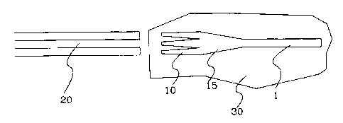
The present invention relates to an optical waveguide (1) comprising a
transition portion in at least one connection end for connection
with an optical component. The transition portion is arranged in such a way
that the waveguide at first changes over into a widening portion
(15) which in turn changes over into a tooth structure (10), where said tooth
structure (10) is intended to be connected to said optical
component.


French Abstract

L'invention concerne un guide d'onde optique (1) comprenant une partie de transition prévue dans au moins une extrémité de connexion à connecter à un composant optique. La partie de transition est conçue de sorte que le guide d'onde change d'abord en partie s'élargissant (15) qui à son tour se modifie en une structure dentée (10) à connecter audit composant optique.

Claims

Note: Claims are shown in the official language in which they were submitted.


7
Claims
1. Optical waveguide (1) comprising a transition portion in at least one
connection end for connection with an optical component, said optical
waveguide
being arranged on a surface (30) of a substrate, and said transition portion
having
a tooth structure (10), where said tooth structure (10) is intended to be
connected
to said optical component, and where the waveguide and its tooth structure are
equally high in relation to the surface (30) of the substrate, characterized
in that
the tooth structure is tapered.
2. Optical waveguide (1) according to claim 1, wherein the transition portion
comprises a widening portion (15), which changes over into the tooth structure
(10).
3. Optical waveguide according to Claim 1 or 2, characterized in that the
widening portion (15) is arranged in a plane which is parallel to the surface
(30)
of the substrate where the waveguide is arranged
4. Optical waveguide according to Claim 3, characterized in that the waveguide
(1) with the widening portion (15) and the tooth structure (10) are equally
high in
relation to the surface (30) of the substrate on which they are arranged.
5. Optical waveguide (1) according to Claim 4, characterized in that the
material
in the waveguide is polymer.
6. Optical waveguide (1) according to Claim 4, characterized in that the
material
in the waveguide is of semiconductor type.
7 Optical waveguide (1) according to Claim 4, characterized in that the
material
in the waveguide is quartz.
8. Optical waveguide according to Claim 5, 6 or 7, characterized in that the
tooth
structure (10) comprises at least two teeth.

8
9. Optical waveguide (1) according to Claim 8, characterized in that the teeth
in
the tooth structure (10) are identical in shape and size in relation to each
other.
10. Optical waveguide (1) according to Claim 8, characterized in that the
teeth in
the tooth structure (10) have different shapes and size in relation to each
other.
11. Optical waveguide according to Claim 9 or 10, characterized in that each
tooth, in the tooth structure is arranged at a distance in relation to the
adjacent
tooth which is the same for each and all of the teeth in the tooth structure.
12. Optical waveguide according to Claim 9 or 10, characterized in that at
least
one tooth in the tooth structure is arranged at a distance in relation to the
adjacent
tooth which is different in relation to the mutual distance between the other
teeth
in the tooth structure.
13. Optical waveguide according to any of claims 1-12, wherein the tooth
structure (10) compromises at least two teeth, and wherein each tooth is
tapered.

Description

Note: Descriptions are shown in the official language in which they were submitted.


CA 02282328 1999-08-30
WO 98/39678 1 PCT/SE98/00327
Optical device
Te~;hnical field
The present invention relates to an optical waveguide having a structure which
facilitates and improves its connection to an optical fiber.
State of the art
One of the fundamental requirements in the construction of communication
network
systems comprising optoelectronic components is that a connection between
these
to a single mode fiber should take place with so small a loss as possible. In
general,
most of a connection loss depends on the difference in size between the
optical fiber
and the waveguide. When the optical waveguide is made of a semiconductor mate-
rial, the loss at the interface between the waveguide and the fiber can, in
certain
cases, be as much as 10 dB.
By increasing the dimension of the optical field of the waveauide a better
corre-
spondence with the optical field of the fiber is achieved, whereby the
connection
loss in the interface between waveguide and fiber is reduced. A number of
different
arrangements and processes to increase the optical field of the waveguide are
known.
One way of converting the optical field in the waveguide is to arrange lenses
in the
interface between the fiber and the waveguide. This method is, however, rather
impractical.
Another way of achieving the above mentioned converting is to transform the
dimensions of the waveguide in the interface with the fiber. Said
transformation

CA 02282328 1999-08-30
WO 98/39678 PCT/SE98/00327
~
is generally called tapering. Tapering can occur either through the dimension
of
the waveguide being increased or reduced in order to increase the optical
field.
Minimizing the dimension is, however, connected with practical difficulties
when
the dimension of the sinale mode waveguide is tremendously small to begin
with.
A more common way is therefore to increase the dimension of the waveguide.
This
increase in the dimension can take place laterally, vertically or laterally
and verti-
cally together, where the vertical tapering can comprise complicated process
steps
which make manufacturing relatively expensive.
Disclosure of the invention
In a transition from a waveguide, defined for example in a or some
semiconductor
materials or some polymer material, to an optical fiber, there are many
factors
which play a decisive role in maintaining the intensity of the light. One of
these
factors is how the optical fields of the waveguide and the optical fiber are
adapted
to each other.
The solutions which are available today often solve said problem through
increasing
the dimension of the waveQuide in the connection to the fiber. Said increase
in the
dimension is required both laterally and vertically in relation to an optical
axis
defined in the waveguide in order for the adaption of the field to be
satisfactory.
From a process point of view said increase in the dimension of the waveguide
is
relatively complicated, especially in the vertical direction, which can be a
problem.
The present invention tackles the above mentioned problem through the
waveguide
being arranged with a so-called tooth-structure in its connection with the
fiber.
The structure of the waveguide in its connection with the fiber can thereby be
said
to be a combination of both a so-called up-tapering and a down-tapering. By up-
. .. _..-_.__...d............._... .. . . . . ...... . . .. .... . I ... .....
. .. . . ........ ..........-.... _ ..._....... . . . . . ... . .. .

CA 02282328 1999-08-30
WO 98/39678 PCT/SE98/00327
3
tapering is meant that the dimension is increased in at least one orthogonal
direction
towards the so-called optical axis defined in the waveguide, and with down-
tapering
is meant that the dimension is miminized in at least one orthogonal direction
towards said optical axis.
The physical effect of an up-tapering in an orthogonal direction in relation
to the
optical axis is that the optical field increases in the same direction as the
up-tapering
and that the optical field in the other orthogonal direction towards the
optical axis
remains relatively undisturbed.
The physical effect of a down-tapering in an orthogonal direction in relation
to the
optical axis is that the optical field increases in both the orthogonal
directions to-
wards the optical axis, if said down-tapering makes the cross-section of the
wave-
guide become sufficiently small. The optical field increases, seen relatively,
more
in the tapered direction, in this case the narrowing direction, compared with
the
untapered.
By means of said structure, when connecting the waveguide to the fiber, an
increase
in the optical field in both orthogonal directions towards the optical axis is
obtained
without it being necessary for this purpose to chanae the dimension in both
said
orthogonal directions.
The purpose of the present invention is to increase the optical field in a
waveguide
in both orthogonal directions in relation to the optical axis through onlv
rearranging
the size and structure in one of said orthogonal directions.
An advantage of the present invention is that the connection loss can be held
to a
low level.

CA 02282328 1999-08-30
WO 98/39678 4 PCT/SE98/00327
Another advantage of the present invention is that aligning the optical fiber
and
the optical waveguide can be facilitated.
Yet another advantage of the present invention is that production can be
relatively
cheap.
A further advantage of the present invention is that it can be applied to
waveguides
manufactured from semiconductor material, polymer material and quartz.
The invention will now be described in more detail with the help of preferred
embodiments and with reference to the appended drawinQ.
Description of the Figures
Figure 1 shows a view from above of a first embodiment of the invention.
FiQure 2 shows a lateral view of the invention according to Figures 1 and 3.
Figure 3 shows a view from above of a second embodiment of the invention.
Preferred embodiments
Figure 1 shows a view from above of a waveguide I according to the invention.
The waveguide I is arranged at one end with a transition portion in order to
increase
the optical field from the waveguide. The transition portion comprises a first
part in
which the waveguide is widened in a plane which corresponds to a surface on a
sub-
strate on which the waveguide is arranged. The widenina 15 in turn changes
over
into a tooth structure 10. The above mentioned transition portion consequently
comprises the widenino, 15 and the tooth structure 10. This can generally be
called
a "taper'".

CA 02282328 1999-08-30
WO 98/39678 PCT/SE98/00327
The above mentioned widening portion 15 can, for example. be parabolic or
linearlv
shaped.
The number of teeth in the tooth structure 10 in Figure I is three. This
number is
5 naturally only an example, however the number should be at least two in
order to
achieve the required changes in the optical field of the waveguide 1 and in
order not
to lose the simplicity in aligning against, for example, an optical fiber 20.
Said teeth
can be given different shapes. What is common for them is that they all have a
shape which in the main is conical. It is conceivable that certain teeth in
the tooth
structure are given a different shape in relation to the others.
The free end of each tooth can either be pointed or flat.
The distance beriveen each tooth in the tooth structure 10 in Fiaure 1 is the
same.
It is naturally possible to arrange a tooth structure 10 in which the
distances between
different adjacent teeth have different mutual distances in relation to each
other.
Figure 2 is a view from the side of the same waveguide 1 which is shown in
Figure
1. This Figure shows that the waveguide 1, the widening and the tooth
structure
have the same height from the surface 30 upon which they are arranged.
The material in the waveguide 1 and thereby the widening 15 and the tooth
structure
10 can be of polymer. quartz or semiconductor type.
Figure 3 shows another embodiment of a waveguide according to the invention.
In this embodiment the waveguide neither tapers up nor tapers down in the
proper
sense. In at least one of the ends of the waveguide a tooth structure is
arranged.
The tooth structure comprises. as mentioned above, preferablv at least two
teeth
so that the simplification of the alignment against another optical unit shall
not be

CA 02282328 1999-08-30
WO 98/39678 PCT/SE98/00327
6
lost. The size and the shape of the teeth can be the same or different. The
distances
between the teeth can be the same or different.
The material in this embodiment can, like the other embodiments, be of quartz,
polymer or semiconductor type.
The process for manufacturing these waveguides can take place through the use
of
techniques wellknown to the man skilled in the art and therefore does not need
to
be described more closely.
The invention is naturally not limited to the embodiments described above and
shown in the drawings but can be modified within the scope of the appended
claims.
. __ . ~._ .

Representative Drawing
A single figure which represents the drawing illustrating the invention.
Administrative Status

2024-08-01:As part of the Next Generation Patents (NGP) transition, the Canadian Patents Database (CPD) now contains a more detailed Event History, which replicates the Event Log of our new back-office solution.

Please note that "Inactive:" events refers to events no longer in use in our new back-office solution.

For a clearer understanding of the status of the application/patent presented on this page, the site Disclaimer , as well as the definitions for Patent , Event History , Maintenance Fee  and Payment History  should be consulted.

Event History

Description Date
Time Limit for Reversal Expired 2017-02-24
Letter Sent 2016-02-24
Grant by Issuance 2007-05-15
Inactive: Cover page published 2007-05-14
Inactive: Final fee received 2007-02-21
Pre-grant 2007-02-21
Letter Sent 2006-09-28
Notice of Allowance is Issued 2006-09-28
Inactive: Approved for allowance (AFA) 2006-05-04
Amendment Received - Voluntary Amendment 2006-04-10
Inactive: S.30(2) Rules - Examiner requisition 2005-10-11
Revocation of Agent Requirements Determined Compliant 2004-11-22
Appointment of Agent Requirements Determined Compliant 2004-11-22
Inactive: Office letter 2004-11-19
Letter Sent 2003-01-15
Request for Examination Received 2002-11-22
Request for Examination Requirements Determined Compliant 2002-11-22
All Requirements for Examination Determined Compliant 2002-11-22
Inactive: Cover page published 1999-11-01
Inactive: First IPC assigned 1999-10-26
Letter Sent 1999-10-07
Inactive: Notice - National entry - No RFE 1999-10-07
Application Received - PCT 1999-10-01
Application Published (Open to Public Inspection) 1998-09-11

Abandonment History

There is no abandonment history.

Maintenance Fee

The last payment was received on 2007-01-24

Note : If the full payment has not been received on or before the date indicated, a further fee may be required which may be one of the following

  • the reinstatement fee;
  • the late payment fee; or
  • additional fee to reverse deemed expiry.

Patent fees are adjusted on the 1st of January every year. The amounts above are the current amounts if received by December 31 of the current year.
Please refer to the CIPO Patent Fees web page to see all current fee amounts.

Owners on Record

Note: Records showing the ownership history in alphabetical order.

Current Owners on Record
TELEFONAKTIEBOLAGET LM ERICSSON
Past Owners on Record
PER JOHAN OLOF SVENSSON
PER OLOV GRANESTRAND
Past Owners that do not appear in the "Owners on Record" listing will appear in other documentation within the application.
Documents

To view selected files, please enter reCAPTCHA code :


To view images, click a link in the Document Description column. To download the documents, select one or more checkboxes in the first column and then click the "Download Selected in PDF format (Zip Archive)" or the "Download Selected as Single PDF" button.

List of published and non-published patent-specific documents on the CPD .

If you have any difficulty accessing content, you can call the Client Service Centre at 1-866-997-1936 or send them an e-mail at CIPO Client Service Centre.


Document
Description 
Date
(yyyy-mm-dd) 
Number of pages   Size of Image (KB) 
Representative drawing 1999-10-31 1 4
Drawings 1999-08-29 1 14
Claims 1999-08-29 3 101
Abstract 1999-08-29 1 47
Description 1999-08-29 6 222
Claims 2006-04-09 2 63
Representative drawing 2007-04-25 1 4
Reminder of maintenance fee due 1999-10-25 1 111
Notice of National Entry 1999-10-06 1 193
Courtesy - Certificate of registration (related document(s)) 1999-10-06 1 115
Reminder - Request for Examination 2002-10-27 1 115
Acknowledgement of Request for Examination 2003-01-14 1 173
Commissioner's Notice - Application Found Allowable 2006-09-27 1 161
Maintenance Fee Notice 2016-04-05 1 170
PCT 1999-08-29 7 267
Correspondence 2004-10-20 3 90
Correspondence 2004-11-18 1 8
Correspondence 2004-11-21 1 13
Correspondence 2007-02-20 1 26