Sélection de la langue

Search

Sommaire du brevet 2282328 

Énoncé de désistement de responsabilité concernant l'information provenant de tiers

Une partie des informations de ce site Web a été fournie par des sources externes. Le gouvernement du Canada n'assume aucune responsabilité concernant la précision, l'actualité ou la fiabilité des informations fournies par les sources externes. Les utilisateurs qui désirent employer cette information devraient consulter directement la source des informations. Le contenu fourni par les sources externes n'est pas assujetti aux exigences sur les langues officielles, la protection des renseignements personnels et l'accessibilité.

Disponibilité de l'Abrégé et des Revendications

L'apparition de différences dans le texte et l'image des Revendications et de l'Abrégé dépend du moment auquel le document est publié. Les textes des Revendications et de l'Abrégé sont affichés :

  • lorsque la demande peut être examinée par le public;
  • lorsque le brevet est émis (délivrance).
(12) Brevet: (11) CA 2282328
(54) Titre français: DISPOSITIF OPTIQUE
(54) Titre anglais: OPTICAL DEVICE
Statut: Périmé et au-delà du délai pour l’annulation
Données bibliographiques
(51) Classification internationale des brevets (CIB):
  • G02B 06/30 (2006.01)
(72) Inventeurs :
  • GRANESTRAND, PER OLOV (Suède)
  • SVENSSON, PER JOHAN OLOF (Suède)
(73) Titulaires :
  • TELEFONAKTIEBOLAGET LM ERICSSON
(71) Demandeurs :
  • TELEFONAKTIEBOLAGET LM ERICSSON (Suède)
(74) Agent: ERICSSON CANADA PATENT GROUP
(74) Co-agent:
(45) Délivré: 2007-05-15
(86) Date de dépôt PCT: 1998-02-24
(87) Mise à la disponibilité du public: 1998-09-11
Requête d'examen: 2002-11-22
Licence disponible: S.O.
Cédé au domaine public: S.O.
(25) Langue des documents déposés: Anglais

Traité de coopération en matière de brevets (PCT): Oui
(86) Numéro de la demande PCT: PCT/SE1998/000327
(87) Numéro de publication internationale PCT: SE1998000327
(85) Entrée nationale: 1999-08-30

(30) Données de priorité de la demande:
Numéro de la demande Pays / territoire Date
9700754-6 (Suède) 1997-03-03

Abrégés

Abrégé français

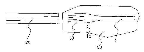
L'invention concerne un guide d'onde optique (1) comprenant une partie de transition prévue dans au moins une extrémité de connexion à connecter à un composant optique. La partie de transition est conçue de sorte que le guide d'onde change d'abord en partie s'élargissant (15) qui à son tour se modifie en une structure dentée (10) à connecter audit composant optique.


Abrégé anglais


The present invention relates to an optical waveguide (1) comprising a
transition portion in at least one connection end for connection
with an optical component. The transition portion is arranged in such a way
that the waveguide at first changes over into a widening portion
(15) which in turn changes over into a tooth structure (10), where said tooth
structure (10) is intended to be connected to said optical
component.

Revendications

Note : Les revendications sont présentées dans la langue officielle dans laquelle elles ont été soumises.


7
Claims
1. Optical waveguide (1) comprising a transition portion in at least one
connection end for connection with an optical component, said optical
waveguide
being arranged on a surface (30) of a substrate, and said transition portion
having
a tooth structure (10), where said tooth structure (10) is intended to be
connected
to said optical component, and where the waveguide and its tooth structure are
equally high in relation to the surface (30) of the substrate, characterized
in that
the tooth structure is tapered.
2. Optical waveguide (1) according to claim 1, wherein the transition portion
comprises a widening portion (15), which changes over into the tooth structure
(10).
3. Optical waveguide according to Claim 1 or 2, characterized in that the
widening portion (15) is arranged in a plane which is parallel to the surface
(30)
of the substrate where the waveguide is arranged
4. Optical waveguide according to Claim 3, characterized in that the waveguide
(1) with the widening portion (15) and the tooth structure (10) are equally
high in
relation to the surface (30) of the substrate on which they are arranged.
5. Optical waveguide (1) according to Claim 4, characterized in that the
material
in the waveguide is polymer.
6. Optical waveguide (1) according to Claim 4, characterized in that the
material
in the waveguide is of semiconductor type.
7 Optical waveguide (1) according to Claim 4, characterized in that the
material
in the waveguide is quartz.
8. Optical waveguide according to Claim 5, 6 or 7, characterized in that the
tooth
structure (10) comprises at least two teeth.

8
9. Optical waveguide (1) according to Claim 8, characterized in that the teeth
in
the tooth structure (10) are identical in shape and size in relation to each
other.
10. Optical waveguide (1) according to Claim 8, characterized in that the
teeth in
the tooth structure (10) have different shapes and size in relation to each
other.
11. Optical waveguide according to Claim 9 or 10, characterized in that each
tooth, in the tooth structure is arranged at a distance in relation to the
adjacent
tooth which is the same for each and all of the teeth in the tooth structure.
12. Optical waveguide according to Claim 9 or 10, characterized in that at
least
one tooth in the tooth structure is arranged at a distance in relation to the
adjacent
tooth which is different in relation to the mutual distance between the other
teeth
in the tooth structure.
13. Optical waveguide according to any of claims 1-12, wherein the tooth
structure (10) compromises at least two teeth, and wherein each tooth is
tapered.

Description

Note : Les descriptions sont présentées dans la langue officielle dans laquelle elles ont été soumises.


CA 02282328 1999-08-30
WO 98/39678 1 PCT/SE98/00327
Optical device
Te~;hnical field
The present invention relates to an optical waveguide having a structure which
facilitates and improves its connection to an optical fiber.
State of the art
One of the fundamental requirements in the construction of communication
network
systems comprising optoelectronic components is that a connection between
these
to a single mode fiber should take place with so small a loss as possible. In
general,
most of a connection loss depends on the difference in size between the
optical fiber
and the waveguide. When the optical waveguide is made of a semiconductor mate-
rial, the loss at the interface between the waveguide and the fiber can, in
certain
cases, be as much as 10 dB.
By increasing the dimension of the optical field of the waveauide a better
corre-
spondence with the optical field of the fiber is achieved, whereby the
connection
loss in the interface between waveguide and fiber is reduced. A number of
different
arrangements and processes to increase the optical field of the waveguide are
known.
One way of converting the optical field in the waveguide is to arrange lenses
in the
interface between the fiber and the waveguide. This method is, however, rather
impractical.
Another way of achieving the above mentioned converting is to transform the
dimensions of the waveguide in the interface with the fiber. Said
transformation

CA 02282328 1999-08-30
WO 98/39678 PCT/SE98/00327
~
is generally called tapering. Tapering can occur either through the dimension
of
the waveguide being increased or reduced in order to increase the optical
field.
Minimizing the dimension is, however, connected with practical difficulties
when
the dimension of the sinale mode waveguide is tremendously small to begin
with.
A more common way is therefore to increase the dimension of the waveguide.
This
increase in the dimension can take place laterally, vertically or laterally
and verti-
cally together, where the vertical tapering can comprise complicated process
steps
which make manufacturing relatively expensive.
Disclosure of the invention
In a transition from a waveguide, defined for example in a or some
semiconductor
materials or some polymer material, to an optical fiber, there are many
factors
which play a decisive role in maintaining the intensity of the light. One of
these
factors is how the optical fields of the waveguide and the optical fiber are
adapted
to each other.
The solutions which are available today often solve said problem through
increasing
the dimension of the waveQuide in the connection to the fiber. Said increase
in the
dimension is required both laterally and vertically in relation to an optical
axis
defined in the waveguide in order for the adaption of the field to be
satisfactory.
From a process point of view said increase in the dimension of the waveguide
is
relatively complicated, especially in the vertical direction, which can be a
problem.
The present invention tackles the above mentioned problem through the
waveguide
being arranged with a so-called tooth-structure in its connection with the
fiber.
The structure of the waveguide in its connection with the fiber can thereby be
said
to be a combination of both a so-called up-tapering and a down-tapering. By up-
. .. _..-_.__...d............._... .. . . . . ...... . . .. .... . I ... .....
. .. . . ........ ..........-.... _ ..._....... . . . . . ... . .. .

CA 02282328 1999-08-30
WO 98/39678 PCT/SE98/00327
3
tapering is meant that the dimension is increased in at least one orthogonal
direction
towards the so-called optical axis defined in the waveguide, and with down-
tapering
is meant that the dimension is miminized in at least one orthogonal direction
towards said optical axis.
The physical effect of an up-tapering in an orthogonal direction in relation
to the
optical axis is that the optical field increases in the same direction as the
up-tapering
and that the optical field in the other orthogonal direction towards the
optical axis
remains relatively undisturbed.
The physical effect of a down-tapering in an orthogonal direction in relation
to the
optical axis is that the optical field increases in both the orthogonal
directions to-
wards the optical axis, if said down-tapering makes the cross-section of the
wave-
guide become sufficiently small. The optical field increases, seen relatively,
more
in the tapered direction, in this case the narrowing direction, compared with
the
untapered.
By means of said structure, when connecting the waveguide to the fiber, an
increase
in the optical field in both orthogonal directions towards the optical axis is
obtained
without it being necessary for this purpose to chanae the dimension in both
said
orthogonal directions.
The purpose of the present invention is to increase the optical field in a
waveguide
in both orthogonal directions in relation to the optical axis through onlv
rearranging
the size and structure in one of said orthogonal directions.
An advantage of the present invention is that the connection loss can be held
to a
low level.

CA 02282328 1999-08-30
WO 98/39678 4 PCT/SE98/00327
Another advantage of the present invention is that aligning the optical fiber
and
the optical waveguide can be facilitated.
Yet another advantage of the present invention is that production can be
relatively
cheap.
A further advantage of the present invention is that it can be applied to
waveguides
manufactured from semiconductor material, polymer material and quartz.
The invention will now be described in more detail with the help of preferred
embodiments and with reference to the appended drawinQ.
Description of the Figures
Figure 1 shows a view from above of a first embodiment of the invention.
FiQure 2 shows a lateral view of the invention according to Figures 1 and 3.
Figure 3 shows a view from above of a second embodiment of the invention.
Preferred embodiments
Figure 1 shows a view from above of a waveguide I according to the invention.
The waveguide I is arranged at one end with a transition portion in order to
increase
the optical field from the waveguide. The transition portion comprises a first
part in
which the waveguide is widened in a plane which corresponds to a surface on a
sub-
strate on which the waveguide is arranged. The widenina 15 in turn changes
over
into a tooth structure 10. The above mentioned transition portion consequently
comprises the widenino, 15 and the tooth structure 10. This can generally be
called
a "taper'".

CA 02282328 1999-08-30
WO 98/39678 PCT/SE98/00327
The above mentioned widening portion 15 can, for example. be parabolic or
linearlv
shaped.
The number of teeth in the tooth structure 10 in Figure I is three. This
number is
5 naturally only an example, however the number should be at least two in
order to
achieve the required changes in the optical field of the waveguide 1 and in
order not
to lose the simplicity in aligning against, for example, an optical fiber 20.
Said teeth
can be given different shapes. What is common for them is that they all have a
shape which in the main is conical. It is conceivable that certain teeth in
the tooth
structure are given a different shape in relation to the others.
The free end of each tooth can either be pointed or flat.
The distance beriveen each tooth in the tooth structure 10 in Fiaure 1 is the
same.
It is naturally possible to arrange a tooth structure 10 in which the
distances between
different adjacent teeth have different mutual distances in relation to each
other.
Figure 2 is a view from the side of the same waveguide 1 which is shown in
Figure
1. This Figure shows that the waveguide 1, the widening and the tooth
structure
have the same height from the surface 30 upon which they are arranged.
The material in the waveguide 1 and thereby the widening 15 and the tooth
structure
10 can be of polymer. quartz or semiconductor type.
Figure 3 shows another embodiment of a waveguide according to the invention.
In this embodiment the waveguide neither tapers up nor tapers down in the
proper
sense. In at least one of the ends of the waveguide a tooth structure is
arranged.
The tooth structure comprises. as mentioned above, preferablv at least two
teeth
so that the simplification of the alignment against another optical unit shall
not be

CA 02282328 1999-08-30
WO 98/39678 PCT/SE98/00327
6
lost. The size and the shape of the teeth can be the same or different. The
distances
between the teeth can be the same or different.
The material in this embodiment can, like the other embodiments, be of quartz,
polymer or semiconductor type.
The process for manufacturing these waveguides can take place through the use
of
techniques wellknown to the man skilled in the art and therefore does not need
to
be described more closely.
The invention is naturally not limited to the embodiments described above and
shown in the drawings but can be modified within the scope of the appended
claims.
. __ . ~._ .

Dessin représentatif
Une figure unique qui représente un dessin illustrant l'invention.
États administratifs

2024-08-01 : Dans le cadre de la transition vers les Brevets de nouvelle génération (BNG), la base de données sur les brevets canadiens (BDBC) contient désormais un Historique d'événement plus détaillé, qui reproduit le Journal des événements de notre nouvelle solution interne.

Veuillez noter que les événements débutant par « Inactive : » se réfèrent à des événements qui ne sont plus utilisés dans notre nouvelle solution interne.

Pour une meilleure compréhension de l'état de la demande ou brevet qui figure sur cette page, la rubrique Mise en garde , et les descriptions de Brevet , Historique d'événement , Taxes périodiques et Historique des paiements devraient être consultées.

Historique d'événement

Description Date
Le délai pour l'annulation est expiré 2017-02-24
Lettre envoyée 2016-02-24
Accordé par délivrance 2007-05-15
Inactive : Page couverture publiée 2007-05-14
Inactive : Taxe finale reçue 2007-02-21
Préoctroi 2007-02-21
Lettre envoyée 2006-09-28
Un avis d'acceptation est envoyé 2006-09-28
Inactive : Approuvée aux fins d'acceptation (AFA) 2006-05-04
Modification reçue - modification volontaire 2006-04-10
Inactive : Dem. de l'examinateur par.30(2) Règles 2005-10-11
Exigences relatives à la révocation de la nomination d'un agent - jugée conforme 2004-11-22
Exigences relatives à la nomination d'un agent - jugée conforme 2004-11-22
Inactive : Lettre officielle 2004-11-19
Lettre envoyée 2003-01-15
Requête d'examen reçue 2002-11-22
Exigences pour une requête d'examen - jugée conforme 2002-11-22
Toutes les exigences pour l'examen - jugée conforme 2002-11-22
Inactive : Page couverture publiée 1999-11-01
Inactive : CIB en 1re position 1999-10-26
Lettre envoyée 1999-10-07
Inactive : Notice - Entrée phase nat. - Pas de RE 1999-10-07
Demande reçue - PCT 1999-10-01
Demande publiée (accessible au public) 1998-09-11

Historique d'abandonnement

Il n'y a pas d'historique d'abandonnement

Taxes périodiques

Le dernier paiement a été reçu le 2007-01-24

Avis : Si le paiement en totalité n'a pas été reçu au plus tard à la date indiquée, une taxe supplémentaire peut être imposée, soit une des taxes suivantes :

  • taxe de rétablissement ;
  • taxe pour paiement en souffrance ; ou
  • taxe additionnelle pour le renversement d'une péremption réputée.

Les taxes sur les brevets sont ajustées au 1er janvier de chaque année. Les montants ci-dessus sont les montants actuels s'ils sont reçus au plus tard le 31 décembre de l'année en cours.
Veuillez vous référer à la page web des taxes sur les brevets de l'OPIC pour voir tous les montants actuels des taxes.

Titulaires au dossier

Les titulaires actuels et antérieures au dossier sont affichés en ordre alphabétique.

Titulaires actuels au dossier
TELEFONAKTIEBOLAGET LM ERICSSON
Titulaires antérieures au dossier
PER JOHAN OLOF SVENSSON
PER OLOV GRANESTRAND
Les propriétaires antérieurs qui ne figurent pas dans la liste des « Propriétaires au dossier » apparaîtront dans d'autres documents au dossier.
Documents

Pour visionner les fichiers sélectionnés, entrer le code reCAPTCHA :


Pour visualiser une image, cliquer sur un lien dans la colonne description du document. Pour télécharger l'image (les images), cliquer l'une ou plusieurs cases à cocher dans la première colonne et ensuite cliquer sur le bouton "Télécharger sélection en format PDF (archive Zip)" ou le bouton "Télécharger sélection (en un fichier PDF fusionné)".

Liste des documents de brevet publiés et non publiés sur la BDBC .

Si vous avez des difficultés à accéder au contenu, veuillez communiquer avec le Centre de services à la clientèle au 1-866-997-1936, ou envoyer un courriel au Centre de service à la clientèle de l'OPIC.


Description du
Document 
Date
(aaaa-mm-jj) 
Nombre de pages   Taille de l'image (Ko) 
Dessin représentatif 1999-10-31 1 4
Dessins 1999-08-29 1 14
Revendications 1999-08-29 3 101
Abrégé 1999-08-29 1 47
Description 1999-08-29 6 222
Revendications 2006-04-09 2 63
Dessin représentatif 2007-04-25 1 4
Rappel de taxe de maintien due 1999-10-25 1 111
Avis d'entree dans la phase nationale 1999-10-06 1 193
Courtoisie - Certificat d'enregistrement (document(s) connexe(s)) 1999-10-06 1 115
Rappel - requête d'examen 2002-10-27 1 115
Accusé de réception de la requête d'examen 2003-01-14 1 173
Avis du commissaire - Demande jugée acceptable 2006-09-27 1 161
Avis concernant la taxe de maintien 2016-04-05 1 170
PCT 1999-08-29 7 267
Correspondance 2004-10-20 3 90
Correspondance 2004-11-18 1 8
Correspondance 2004-11-21 1 13
Correspondance 2007-02-20 1 26