Note: Descriptions are shown in the official language in which they were submitted.
CA 02282419 1999-09-02
WO 98/41054 PCT/SE98/00373
1
TIME SWITCH STAGES AND SWITCHES
TECHNICAL FIELD OF THE INVENTION
The invention relates to switches and switch stages forming part of
V
telecommunication systems. More specifically, the invention relates to
establishing connections through digital circuit-switching switches.
BACKGROUND OF THE D1YENTION
User data switched through a digital switch belong to channels, so called
connections. In the switch, user data originating from each connection from a
respective input in the switch are switched to a respective selectable output
in
the switch. A technique used in connection thereto is circuit switching. A
common switch structure in circuit switching is called "Time Space Time"
(TST).
In switches having this structure, a plurality of time switch stages are
connected to a space switch stage. User data is first switched through an
incoming time switch stage, then through a space switch stage and finally
through an outgoing time switch stage.
User data from several connections that are to be switched through a switch of
TST-structure are multiplexed by means of time multiplexing. In time
multiplexing, the user data is placed in time slots that are arranged in
frames.
In switching the user data through the switch, it is moved between different
time slots and frames. This is accomplished by delaying the user data in
memories, so called speech memories, in the time switch stages of the switch.
A
speech memory comprises storage positions for storing user data. Each storage
position corresponds to a time slot and stores, during a certain time, a data
word of the user data, such as a byte. In addition to the speech memories, the
time switch stages also include control memories and time slot counters by
means of which writing of the user data into, and reading of the user data out
of
the speech memories are performed in different time slots. A control memory
also includes storage positions, each of which corresponds to a time slot. A
time
slot counter cyclically addresses storage positions in the control memory as
well
CA 02282419 1999-09-02
WO 98/41054 PCT/SE98100373
2
as in the speech memory. For each time slot, a storage position in the control
memory is addressed for reading control information stored in the control
memory. The control information in the control memories in turn addresses the
speech memories for reading the user data from the incoming time switch
stages on one hand, and for writing the user data into the outgoing time
switch
stages on the other hand.
User data arriving to an incoming time switch stage appears in incoming time
slots. In the space switch stage, the user data is placed by the incoming time
switch stage in so called internal time slots. The user data going out from an
outgoing time switch stage is placed by the outgoing time switch stage in
outgoing time slots. Conflict in the space switch stage is avoided by means of
the internal time slots.
Control information is generated in a control system, such as a computer
program-controlled control system, being part of the telecommunication system.
The control system is connected to the switch. Writing of control information
into the control memories is instructed from the control system for assigning
time slots used in the switching of the user data through the switch.
In one type of connection, a so called narrowband connection, user data
arrives
in a single incoming time slot each frame. User data are delayed differently
for
different narrowband connections. For each narrowband connection, the delay
depends on in which incoming time slots that user data arrives to the switch,
and in which internal time slots and outgoing time slots that user data for
the
narrowband connection are switched through the switch. The reciprocal timing
relations between the incoming time slots, the internal time slots and the
outgoing time slots for a narrowband connection determines the delay of the
user data belonging to the narrowband connection.
Another type of connection, a so called wideband connection, occupies several
time slots in each frame. User data belonging to a wideband connection arnves
CA 02282419 1999-09-02
WO 98/41054 PCT/SE98/00373
3
in several incoming time slots in each frame, and is switched through the
switch
in several internal time slots and in several outgoing time slots, in a sense
as
several separate narrowband connections. Thus, a wideband connection may be
considered as an association of several narrowband connections. User data
belonging to a wideband connection will consequently be switched through the
switch in several narrowband connections with different delays.
A problem in connection thereto is to obtain sequence integrity, so called
Time
Slot Sequence Integrity (TSSI), and frame integrity, so called Time Slot Frame
Integrity (TSFI), for wideband connections, i.e. to assure that data words
constituting user data for a wideband connection maintain one and the same
reciprocal time order through the switch on one hand, and that those data
words that arrive in incoming time slots in one and the same frame are placed
in the same frame in outgoing time slots on the other hand.
If as an example frame integrity (TSFI) is not preserved through the switch,
then
the user terminals in some telecommunication applications have to be equipped
with frame analysis and frame regeneration equipment. This means an
undesirable increased cost for the users.
U.S. Patent 4,809,259 to Jonsson discloses an arrangement for establishing a
wideband connection in a switching network. A marking device is disposed at
the input of the switching network to provide markings in successive frames of
the respective contents of the time slots utilized by the connection channels
such that each affected time slot in a first frame is assigned a first marking
and
each affected time slot in a second frame is assigned a second marking. A
scanning device is disposed at the output of the switching network to detect
the
markings such that a possible delay between the respective contents of the
- channels can be determined. Furthermore, the scanning device controls a
delay
equalizing device in the channels. The equalizing device comprises at least
two
paths for the flow of data from the switching network, a first path being a
direct
path without delay, a second path having a delay memory in the form of a
CA 02282419 1999-09-02
WO 98/41054 PC"f/SE98/00373
4
register that delays data one frame, a third path delaying the data two
frames,
and so on. The scanning device provides delay instructions to a control memory
in the equalizing device, and the delay instructions in the control memory
control a selector which determines from which one of the paths data is to be
read.
The Swedish Patent Publication SE-B-461,310 describes a method and device
for switching a wideband connection through a digital time switch. The problem
addressed in the Publication is that some time slots are delayed a frame,
whereas other time slots are not delayed. According to the Swedish Patent
Publication, a processor in the switch determines which outgoing time slots
will
hold information that is delayed one frame, .and which outgoing time slots
will
hold information that is not delayed, and a control memory in the switch is
provided with a marking bit, for each outgoing time slot, that indicates if
the
time slot is delayed or not. Incoming time slots to the digital time switch
are
sequentially written into a first speech memory. The first speech memory is
connected to an additional separate speech memory, and the incoming time
slots stored in the first speech memory are transferred to and written into
the
additional speech memory with a delay of one frame. During each clock pulse,
information stored in a given storage position in the first speech memory is
read
from the first speech memory and written into the additional speech memory in
a corresponding storage position, whereupon information in an incoming time
slot in a subsequent frame is written into the first speech memory at the
given
storage position. Consequently, the additional speech memory will hold
information that is delayed one frame relative to the contents of the first
speech
memory. For each outgoing time slot, information corresponding to the time
slot
is read from the first speech memory as well as from the additional speech
memory and provided to a multiplexor. The multiplexor is controlled by' the
corresponding marking bit in the control memory, and connects a bus for
outgoing time slots either to the first speech memory or to the additional
speech
memory. In this way, the information in delayed time slots will be read from
the
CA 02282419 1999-09-02
WO 98/41054 PCT/SE98/00373
first speech memory and transferred onto the bus, and the information in non-
delayed time slots will be read from the additional speech memory.
The solution of the Swedish Patent Publication SE-B-461,310 implies that all
5 outgoing time slots are delayed an extra frame through the switch. The
number
of necessary memory accesses is increased considerably, since two write
operations and two read operations are required for each time slot in the time
switch. This increases the amount of dissipated power in the digital time
switch.
Read-out is performed only from the storage positions in the additional speech
memory that are associated with a wideband connection. This means that a
malfunctioning storage position in the additional speech memory is not
detected
until a wideband connection that utilizes that particular storage position is
actually established. Consequently, it is not possible to continuously monitor
the storage positions of the additional speech memory since parity check of
the
information in these storage positions can only be performed in connection
with
read-out onto the outgoing bus from positions associated with established
wideband connections.
The European Patent Application 0,532,914 A2 relates to a delay correcting
system in a multi-channel PCM-switching system. In accordance with this delay
correcting system, an external memory separated from the speech memories in
the switch structure itself, and a control unit for delaying some of the data
stored in this external memory, are utilized. The external memory is provided
at
the output (or the input) of the switch, and the data that have been switched
through the switch are stored after output therefrom in the external memory.
The control unit generates frame correction information of several bits that
is
sent to a complicated circuit. The circuit functions to delay some of the data
stored in the external memory in accordance with the frame correction
_ information such that these data are delayed by the number of frames
indicated
by the most delayed data through the switch. Consequently, data in an outgoing
frame N from the switch can be delayed one or more frames such that these
data are outputted in frame N+ 1, N+2 or N+3 .
CA 02282419 1999-09-02
WO 98/41054 PCT/SE98/00373
6
According to the solution of the European Patent Application 0,532,914 A2,
neither the external memory nor the circuit otherwise is integrated in the
switch structure itself. In addition, the use of an additional external memory
increases the number of necessary memory accesses. Besides, the additional
external memory does not have any continuous monitoring of the storage cells,
since these cells are used only in delay for established wideband connections
and not for narrowband connections.
U.S. Patent 4,704,716 to Bowers et al. discloses a method and device for
establishing a wideband connection comprising a number of segments of TDM-
channels through a communication network. In particular, a switching network
of TST-type is provided with additional buffer memories in the incoming time
stage and the outgoing time stage to assure that all data received in a time
frame from a given segment is assembled only into the same outgoing time
frame. In the incoming stage, two buffer memories are used, where all data in
a
given frame is stored in one of these buffer memories in a given frame period,
at
the same time as read-out of data in the other buffer memory is performed, and
read out of the same buffer memory the next time period, at the same as data
is
stored in the other buffer memory. In the outgoing stage, where the read and
write cycles of a time frame do not coincide because of signal delays in the
switching network, three buffer memories are used in a way corresponding to
that in the incoming time stage to assure that data in a given time frame are
maintained in the same time frame.
This solution results in an extra delay in both the incoming stage and the
outgoing stage. A plurality of additional buffer memories are required, and in
addition, the writing and reading alternately between the different buffer
memories have to be administered in some way.
CA 02282419 1999-09-02
WO 98/41054 PC1'/SE98/00373
7
SUMMARY OF THE INVENTION
A main object of the invention is to find a simple way of obtaining sequence
integrity (TSSI) and frame integrity (TSFI) in switching connections through a
switch or a switch stage.
Further, an object of the invention is to provide a realization which delays
some
data in such a way that the integrity requirements are fulfilled. This
realization
should be integrated in the switch itself in such a way that only a minimum of
extra equipment needs to be used. In addition, it is desirable to be able to
easily
monitor the realization continuously.
A further object of the invention is to obtain sequence and frame integrity
with
minimized delay of the user data through the switch and without increasing the
number of necessary memory accesses.
These objects are met by the invention as defined in the accompanying patent
claims.
User data belonging to a connection, preferably a wideband connection, are
distributed, on one hand, among the internal time slots in each frame that
have
been assigned to the wideband connection for switching the user data through
the switch, and on the other hand among the outgoing time slots in each frame
that have been assigned to the wideband connection for switching the user data
through the switch.
According to a general inventive concept, the speech memory in a switch stage
of the switch is extended such that it includes storage positions that in
number
correspond to the number of time slots in two frames. These storage positions
. are arranged in two memory parts of equal size in the speech memory.
Furthermore, a delay control unit is provided in the time switch stage for
generating delay information based on control information in the control
memory of the switch stage and a determined part of the counter information
CA 02282419 1999-09-02
WO 98/41054 PCT/SE98/00373
8
from a time slot counter circuit. This delay information controls, for each
time
slot, to/from (depending on whether the speech memory is arranged in an
outgoing stage or an incoming stage) which one of the first and second part of
the speech memory that user data is to be switched.
In a specific embodiment of the invention, the control information in the
control
memory of the switch stage includes, for each time slot, first control data
indicating to/from which time slot in a frame that user data is to be
switched,
and second control data representative of whether this user data is to be
switched to the first frame or delayed a frame to the second frame.
The extended speech memory and the delay control unit may be provided in e.g.
an incoming time switch stage or an outgoing time switch stage of the switch.
The inventive idea is particularly applicable to an arbitrary switch stage
through
which user data is switched between first time slots arriving to the stage and
second time slots going out from the stage.
Since an extended speech memory is used without any additional separate
memory unit, the number of memory accesses does not increase. In addition, a
continuous monitoring of all the storage cells in the extended speech memory
is
obtained automatically, since all the cells are cyclically accessed in two
frames;
not only in connection with the delay of wideband connections but all the
time,
also in normal switching of narrowband connections.
By extending the speech memory, the delay values are easy to produce. The
delay values are preferably in the form of a single bit per time slot, stored
in the
control memory of the switch stage in question.
The speech and control memories already available in the switch are optimally
utilized. The solution is thus integrated in the switch structure itself such
that
only a minimum of extra equipment is required.
CA 02282419 1999-09-02
WO 98/41054 PCT/SE98/00373
9
The invention has the following advantages:
- frame and sequence integrity are preserved through a switch by using a
minimum of extra equipment;
- the delay mechanism for obtaining sequence and frame integrity just
needs to be performed on one side of the switch, whereby the delay is
minimized;
- the number of memory accesses does not increase, since the idea is to
extend an already available speech memory;
- the solution is integrated in the switch structure itself;
- a simple logic implementation of the delay control unit;
- the extra control information in form of delay values can be realized by a
single bit per time slot, facilitating the logic implementation and minimizing
the
extra memory space required in the control memory; and
- continuous monitoring of the cells of the extended speech memory is
automatically obtained.
BRIEF DESCRIPTION OF THE DRAWINGS
The invention will now be described in more detail with reference to the
drawings, in which:
Fig. 1 schematically shows a circuit-switching switch having TST-structure and
a control system;
Fig. 2a shows a control system and a time switch module with an outgoing time
switch stage according to the invention;
Fig. 2b shows a control system and a time switch module with an incoming time
switch stage according to the invention;
Fig. 3 shows a time slot counter circuit according to the invention;
Fig. 4 shows a delay control unit according to the invention;
CA 02282419 1999-09-02
WO 98/41054 PCT/SE98/00373
Fig. S shows a flow diagram according to the invention describing how incoming
time slot numbers are normalized against a time phase of frames for internal
time slots;
5 Fig. 6 shows a flow diagram describing how an offset-variable is determined
according to the invention;
Fig. 7a shows a flow diagram according to the invention describing how
distribution information in form of storage positions in the control memories
is
10 determined by using the offset-variable;
Fig. 7b illustrates how the determined offset-variable influences the
distribution
of incoming time slot numbers and outgoing time slot numbers to the storage
positions in the respective control memory;
Fig. 8 shows a flow diagram according to the invention describing how internal
time slots are normalized against a time phase of frames for outgoing time
slots;
Fig. 9 shows a flow diagram according to the invention describing how a base
value is determined;
Fig. 10 shows a flow diagram according to the invention describing a
determination of whether any time slot is associated with a subsequently
following frame relative to the frame represented by the base value;
Fig. 11 shows a flow diagram according to the invention describing a
determination of control information in form of delay values for respective
time
slot numbers in frames for outgoing time slots; and
Fig. 12 is a diagram of frames of incoming time slots, internal time slots and
frames of outgoing time slots, schematically showing how user data in the
incoming time slots are distributed onto the internal time slots and the
outgoing
CA 02282419 1999-09-02
WO 98/41054 PCT/SE98/00373
11
time slots according to an illustrative example of a set-up of a wideband
connection.
DESCRIPTION OF ILLUSTRATIVE EMBODIMENT8
User terminals (not shown), such as telephones and computers, generate and
receive user data. It should be understood that "user terminals" also means
internal equipment of a telecommunication system that generates and/or
receives data, such as trunks, tone senders, tone receivers and conference
units. The user data is made up of data words of e.g. 8 bits. User data to or
from
a group of user terminals appear by means of time multiplexing in one and the
same so called multiplex in time intervals referred to as time slots, which in
turn are part of larger time intervals, of 125 ms, referred to as PCM-frames
or
for simplicity just frames. User data generated by a user terminal and
received
by a (normally another) user terminal is associated with a so called
connection
that is unique for the user data. A multiplex thus includes user data from a
plurality of connections. User data belonging to a connection is arranged in
one
or more time slots in each frame, where the timing relations of the time slots
to
their respective frames do not change between successive frames. The frames
constitute time references by means of which the user data is associated to
the
connections.
In fig. 1 there is shown a telecommunication system having a circuit-switching
switch 1 of the type "Time-Space-Time", a so called TST-switch, and a control
system 2 connected to the switch. The switch 1 has a number of inputs 3.n and
a number of outputs 4.n. For simplicity, only two inputs 3.1, 3.2 and two
outputs 4.1, 4.2 are shown. The switch 1 further includes incoming time switch
stages 5.n and outgoing time switch stages 6.n, which in pairs form part of
time
switch modules 7.n, and a space switch stage 8. For simplicity only two
incoming time switch stages 5.1, 5.2 and two outgoing time switch stages 6.1,
6.2 are shown.
CA 02282419 1999-09-02
WO 98/41054 PCT/SE98/00373
12
Each input 3.n is connected to a respective incoming time switch stage 5.n. To
each outgoing time switch stage 6.n a respective output 4.n is connected. An
input 3.n and an output 4.n that are connected to an incoming time switch
stage 5.n and an outgoing time switch stage 6.n, respectively, in the same
time
switch module 7.n are associated to multiplexes that normally belong to the
same group of user terminals. Outputs 9.n from the incoming time switch
stages are connected to inputs 10.n of the space switch stage 8.n. Outputs l
l.n
of the space switch stage are connected to inputs 12.n of the outgoing time
switch stages 6.n. The connections appear more closely from the figure for
outputs 9.1, 9.2, 11.1, 11.2 and inputs 10.1, 10.2, 12.1, 12.2.
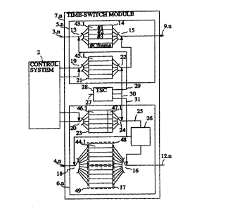
In Fig. 2a, a time switch module 7.n and the control system 2 are shown. The
control system 2 is shown in general, whereas the time switch module 7.n is
shown in more detail. The time switch module 7.n comprises an incoming time
switch stage 5.n and an outgoing time switch stage 6.n. The input 3.n, on
which
a multiplex is arriving from a group of user terminals, is connected to an
addressing unit 13, which in turn is connected to a speech memory 14. The
speech memory 14 is connected to an addressing unit 15 that is connected to
the output 9.n. The input 12.n is connected to an addressing unit 16, which in
turn is connected to a speech memory 17. The speech memory 17 is connected
to an addressing unit 18, which in turn is connected to the output 4.n. The
control system 2 is connected to addressing units 19 and 20. The addressing
unit 19 is connected to a control memory 21. The control memory 21 is
connected to an addressing unit 22. The addressing unit 22 is connected to the
addressing unit 15. The addressing unit 20 is connected to a control memory
23. The control memory 23 is in turn connected to an addressing unit 24. An
output 25 of the addressing unit 24 is connected to a delay control unit 26
which in turn is connected to the addressing unit 16. On an input 27, a clock
signal is coming from a per se known and therefore not shown clock for
generating clock pulses, each of which corresponds to a time slot. The input
27
is connected to a time slot counter (TSC) 28. The time slot counter 28 is
CA 02282419 1999-09-02
WO 98/41054 PCT/SE98/00373
13
connected, via different outputs 29, 30 and 31, to the addressing units 13,
18,
22, 24 on one hand and to the delay control unit 26 on the other hand.
The time slot counter 28 is shown in closer detail in Fig. 3. Except for a
counter
32, per se known, the time slot counter 28 also includes means 33, means 34
and means 35 to which the counter 32 is connected. The output 29 is
associated with means 33 and connected to the addressing unit 13. The output
30 is associated with means 34 and connected to the addressing unit 22 on one
hand and to the addressing unit 24 on the other hand. The output 31 is
associated with means 35 and connected to the addressing unit 18 on one hand
and to the delay control unit 26 on the other hand. The function of means 33,
34 and 35 will be described later on.
The delay control unit 26 is shown in more detail in Fig. 4. An input 36 to
the
delay control unit 26 from the output 25 of the addressing unit 24 is
connected
partly to a first input of a first comparator 37 on one hand, and partly to a
first
input of a first XOR-gate 38 on the other hand. An input 39 to the delay
control
unit 26 from the output 31 of means 35 in the time slot counter 28 is
connected
to means 40 on one hand and to a second comparator 41 on the other hand.
Means 40 is connected to a second input of the first comparator 37. The first
comparator 37 and the second comparator 41 are connected to a respective
input of a second XOR-gate 42. The output from the second XOR-gate 42 is
connected to a second input of the first XOR-gate 38. The first XOR-gate 38 is
in
turn connected to the addressing unit 16. Further, the output 25 from the
addressing unit 24 is partly connected to the addressing unit 16 via the delay
control unit 26.
Referring once again to Figs. 1 and 2a. The user data in the respective
connection is switched through the switch 1 from an input 3.n to a selectable
output 4.n. In this respect, time switching in the time switch stages 5.n, 6.n
as
well as space switching in the space switch stage 8 are performed. The time
switching means that user data arriving to a time switch stage 5.n, 6.n in
given
CA 02282419 1999-09-02
WO 98/41054 PCT/SE98/00373
14
time slots relative to the frames are delayed and goes out of the time switch
stage 5.n, 6.n in other time slots relative to the frames. In space switching,
physical connections such as galvanic connections, are established from the
inputs 10.n of the space switch stage to the outputs ll.n thereof. Space
switching means that user data arriving to the space switch stage 8 on an
input
10.n, e.g. 10.7 (not shown), goes out of the space switch stage 8 from a
selectable output l l.n, e.g. 11.3 (not shown).
In switching user data belonging to a connection through the switch 1, the
user
data arrives in one or more given time slots in each frame, in so called
incoming
time slots, to an incoming time switch stage 5.n. In the incoming time slots,
the
user data is written into the speech memory 14 (Fig. 2a). The user data is
read
out of the speech memory 14 in other time slots, in so called internal time
slots.
The user data thus appearing in internal time slots is physically switched
through the space switch stage 8 (Fig. 1 ) and written, in the internal time
slots,
into the speech memory 17 (Fig. 2a) of an outgoing time switch stage 6.n. In
yet
other time slots, so called outgoing time slots, the user data is read out of
the
speech memory 17.
The writing and reading of user data into and out of the speech memories 14,
17 are controlled by the addressing units 13, 15, 16, 18, which in turn are
controlled by the time slot counter 28 and by the control system 2 through the
addressing units 19, 20, 22, 24, the control memories 21, 23 and the delay
control unit 26.
By means of the time slot counter 28, via the addressing unit 13, user data is
cyclically written into storage positions 43.n in the speech memory 14 in a
fixed
sequence. The number of storage positions 43.n in the speech memory 14 is
equal to the number of time slots in a frame. For simplicity, 5 storage
positions
43.1-43.5 (however, only reference number 43.1 is shown in Fig. 2a) are shown,
which correspond to 5 time slots in a frame. In reality however, the number of
time slots in each frame is in general substantially greater, 512 as an
example.
CA 02282419 1999-09-02
WO 98141054 PCT/SE98/00373
Each storage position 43.n represents one and only one unique time slot in
each
frame. User data arriving in a certain incoming time slot in a frame is
consequently stored in a given storage position 43.n corresponding to the
. incoming time slot. The read-out of user data from the speech memory 17 into
5 outgoing time slots is performed in a similar way. However, in the speech
memory 17 there are twice as many storage positions 44.n as in the speech
memory 14, i.e. as many storage positions 44.n as time slots in two frames. In
the speech memory 17, 10 storage positions 44.1-44.10 (however, only reference
number 44.1 is shown in Fig. 2a) are shown. The read-out of the user data is
10 performed cyclically in a fixed sequence, one storage position 44.n each
outgoing time slot such that each time slot represents a given outgoing time
slot
in every second frame. Consequently, user data can be switched to a time slot
in
an earliest possible outgoing frame or in a subsequently following outgoing
frame.
User data that is assigned a storage position 44.n may selectively be delayed
up
to a time corresponding to two frames, depending on the value of the time slot
counter 28 at the time for writing of the user data and in which storage
position
44.n (the addressing information to the addressing unit 16) that writing of
the
user data is performed.
Now with reference to Fig. 3. The counter 32 that forms part of the time slot
counter 28 cyclically occupies different states in a counter sequence such
that
different counter values are taken. The number of different counter values
taken
by the counter 32 is equal to the number of time slots in two frames. For each
time slot in the two frames, a unique counter value is taken.
In means 33 and 35, values with a so called offset from the counter values are
generated. In the respective means 33, 35 a value, called phase value, is
generated for each counter value. Phase values obtained by means 33 have a
difference compared to the counter values, representing a difference in phase
between frames for internal time slots and frames for incoming time slots.
Phase
CA 02282419 1999-09-02
WO 98/41054 PCT/SE98/00373
16
values obtained by means 35, at the output 31, have a difference compared to
the counter values, representing a difference in phase between frames for
outgoing time slots and frames for internal time slots. In the following, a
phase
value at the output 31 is also called an outgoing phase value. By means of the
phase values, the switch handles reciprocal phase differences between frames
for incoming time slots, frames for internal time slots and frames for
outgoing
time slots.
In means 33 and 34, modulo operations are performed. In means 34 a modulo
operation between the counter value and a value representing the number of
time slots in a frame is performed. By means of the modulo operation, a
sequence of read-out counter values, in number equal to the number of time
slots in a single frame but repeated twice for each counter sequence from the
counter 32, is cyclically generated at the output 30 of means 34. In means 33
a
modulo operation between the phase value and the value representing the
number of time slots in a frame is performed. In that way, counter values
similar to those from means 34, but with an offset, are generated at the
output
29 of means 33. In practice, the modulo operations imply that the most
significant bit of the counter values or phase values is eliminated.
By means of the control system 2 (Figs. 1 and 2a), control information for
controlling the switch 1 is generated. The control information comprises data
words of e.g. 12 bits on one hand, and single bits on the other hand. The data
words are written into storage positions 45.n and 46.n in the control memories
21 and 23, respectively, and the single bits are written into storage
positions
47.n in the control memory 23, 1 bit per storage position 47.n, for
controlling
the switch 1. The bits in the storage positions 47.n are called delay values
or
delay bits in the following. The number of storage positions 45.n, 46.n, 47:n
of
respective type is equal to the number of time slots in a frame. The number of
storage positions 45.n, 46.n, 47.n of each type shown is therefore equal to 5.
By
means of the time slot counter 28, via the addressing units 22, 24, control
information is read out of a storage position 45.n, 46.n, 47.n in respective
CA 02282419 1999-09-02
WO 98/41054 PCT/SE98/00373
17
control memories 21, 23 in each time slot. Read-out is performed cyclically in
a
fixed sequence, one unique storage position 45.n, 46.n, 47.n for the
respective
time slot in a frame. Thus, each storage position 45.n, 46.n, 47.n implicitly
corresponds to one and only one time slot in each frame.
Control information indicating from which storage position in the speech
memory that user data is to be read, and in that way appear in internal time
slots, is read out from the control memory 21 in each time slot. Control
information indicating in which outgoing time slot in a frame that read-out of
the user data is to be performed on one hand and if the user data is to be
read
out in a first possible frame or to be delayed an extra frame on the other
hand,
is read from the control memory 23 in each internal time slot.
The delay control unit 26 (Fig. 4) generates, from the control information
from
the control memory 23, via the addressing unit 24, and from information from
the time slot counter 28, addressing information to the addressing unit 16 for
writing the user data into the speech memory 17. In unit 26, the control
information from the control memory 23 is compared to the information from
the time slot counter 28. The outcome of the comparison results in user data
being written, via the addressing unit 16, into storage positions 44.n either
in a
first part 48 of the speech memory 17 or in a second part 49 of the speech
memory I7.
The delay control unit 26 receives the control information from the storage
positions 46.n, 47.n in the control memory 23 at the input 36. The control
information in the storage positions 46.n is directly applied to the
addressing
unit 16, and forms a first part 50 of the addressing information. The control
information in the storage positions 46.n is also applied to the first input
of the
first comparator 37. The input 39 is provided with the phase values from the
unit 35 which also controls the addressing unit 18 for reading out the user
data
into the outgoing time slots. Via unit 40, which performs a modulo operation
between phase values from the unit 35 and a value representing the number of
CA 02282419 1999-09-02
WO 98/41054 PC"f/SE98/00373
18
time slots in a frame, the second input of the first comparator 37 is provided
with comparison values A representing outgoing time slots in each frame.
If, in a time slot, a comparison value A is greater than the control
information,
i.e. a value B from a storage position 46.n in the control memory 23, a bit
which
constitutes output data of the output of the first comparator 37 is set to
"1".
On the other hand, if the comparison value A is less than or equal to the
control
information B, the bit is set to "0". The bit indicates, if it is set to "1",
that
i. if writing of user data takes place in the first part 48 of the speech
memory 17,
and read-out of user data also takes place in the first part 48 of the speech
memory 17, or
ii. if writing of user data takes place in the second part 49 of the speech
memory
17, and read-out of user data also takes place in the second part 49 of the
speech memory 17,
then the user data is delayed more than one frame, otherwise not.
In the second comparator 41, the outgoing phase value is compared to a value
representing the number of time slots in a frame. If the outgoing phase value
is
greater than the number of time slots in a frame, then a bit that constitutes
output data of the output from the second comparator 41 is set to " 1". On the
other hand, if the outgoing phase value is less than or equal to the number of
time slots in a frame, then the bit is set to "0". The bit indicates, if it is
set to "1",
that read-out of user data in the current time slot is performed from the
second
part 49 of the speech memory 17. If the bit is instead set to "0", it
indicates that
read-out of user data is performed from the first part 48 of the speech memory
17.
A first XOR-operation is performed in the second XOR-gate 42 between the bit
from the first comparator 37 and the bit from the second comparator 41. The
result of the first XOR-operation is a bit at the output of the second XOR-
gate
42 which indicates, if it is set to "1", that writing of user data into the
first part
CA 02282419 1999-09-02
WO 98/41054 PCT/SE98/00373
19
48 of the speech memory 17 in the current time slot results in user data being
delayed more than one frame. If it instead is set to "0", it indicates that
writing
into the second part 49 of the speech memory 17 in the current time slot
results
. in user data being delayed more than one frame.
A second XOR-operation is performed in the first XOR-gate 38 between the bit
from the output of the second XOR-gate 42 and a delay bit from a storage
position 47.n. Delay bits from the storage positions 47.n constitute a second
part 51 of the addressing information. A delay bit indicates, if it is set to
"0",
that user data is to be placed in that part of the speech memory 17, i.e. in
the
first part 48 or in the second part 49, that implies that user data is to be
read
out in time slots in a first possible frame for outgoing time slots. On the
other
hand, if the delay bit is set to "1", it indicates that user data is to be
placed in
that part of the speech memory 17 that implies that the user data is read out
in
time slots in a subsequently following frame.
A bit, so called delay information, at the output of the first XOR-gate 38
indicates, if it is set to "0", that user data is to be written into the first
part 48 of
the speech memory 17, whereas, if set to "1", it indicates that user data is
to be
written into the second part 49 of the speech memory 17. The delay information
in form of a bit from the output of the first XOR-gate 38 controls the
addressing
unit 16 such that writing of the user data takes place either in the first
part 48
of the speech memory 17 or in the second part 49 of the speech memory 17,
based on the control information in the storage positions 46.n, 47.n in the
control memory 23, and based on the outgoing phase value from the time slot
counter 28.
In a so called narrowband connection, the user data for the connection appears
in a single incoming time slot each frame, an internal time slot each frame
and
an outgoing time slot each frame. The control information for the narrowband
connection is written into a storage position 45.n, and into a storage
position
46.n, 47.n. The storage positions 45.n, 46.n, 47.n correspond to the internal
CA 02282419 1999-09-02
WO 98/41054 PCT/SE98/00373
time slots. The control information in the storage positions 45.n indicates
from
which incoming time slots that user data is to be switched to the internal
time
slots, i.e. out of which storage position 43.n that user data is to be read
from the
speech memory 14. The control information in the storage position 46.n, 47.n
5 indicates to which outgoing time slots that user data is to be switched from
the
internal time slots, i.e. in which storage position 44.n that user data is to
be
written into the speech memory 17 such that read-out of the user data takes
place in outgoing time slots for the connection. Consequently, the control
information associated with a narrowband connection includes a value
10 indicating in which incoming time slot the user data arrives to the switch,
a
value indicating in which internal time slot the user data is switched through
the space switch stage, and a value indicating in which outgoing time slot the
user data goes out of the switch. In the following, these values representing
determined timing relations to the frames are called incoming time slot
15 numbers, internal time slot numbers and outgoing time slot numbers,
respectively. In addition to time slot numbers, the control information for a
narrowband connection includes a constant delay value for each time slot,
which is written into the storage position 47.n. The value indicates that the
user
data goes out of the switch in earliest possible frames.
In a so called wideband connection, the user data for the connection is
switched
in several incoming time slots each frame, in several internal time slots each
frame and in several outgoing time slots each frame, in principle as several
narrowband connections. Control information for controlling the switch for a
wideband connection thus includes several incoming time slot numbers, several
internal time slot numbers and several outgoing time slot numbers. In addition
thereto, the control information includes delay values, one for each time slot
in
a frame for the wideband connection, which indicate whether user data is to
appear in earliest possible frames or to be delayed an extra frame in the
outgoing time switch stage. These values are written into the storage
positions
47.n.
CA 02282419 1999-09-02
WO 98/41054 PCT/SE98/00373
21
It should be understood that this aspect of the invention also is applicable
to the
incoming time switch stage. With reference to Fig. 2b, there is shown a switch
structure in form of a time switch module 7.n to which a control system 2 is
connected. The same reference numerals as in Fig. 2a are used to designate the
same or corresponding elements. The difference compared to Fig. 2a is that the
invention is applied to the incoming time switch stage 5.n. The speech memory
14 is extended to include two parts 48 and 49 (for simplicity, the same
reference
numerals as in Fig. 2a are used), each of which contains storage positions
that
in number correspond to the number of time slots in a frame. The control
memory 21 is also extended such that it includes control information in the
storage positions 45.n and control information in form of delay values in the
positions 47.n. The control information from the control memory 21 in the
incoming time switch stage 5.n is fed, via the addressing unit 22, to the
delay
control unit 26 which, in this embodiment, is connected to the addressing unit
15 to control the read-out of user data from the extended speech memory 14.
The delay control unit 26 functions in a way corresponding to that of Fig. 2a,
and here the time slot counter information at the output 29 corresponds to the
information from means 35 in Fig. 2a. In particular, the delay control unit
generates delay information that controls, for each internal time slot, from
which of the first part 48 and the second part 49 of the speech memory 14 that
user data is to be switched to the internal time slot. It should be noted that
according to Fig. 2a, the delay control unit 26 controls the storage of user
data
in the extended speech memory 17, whereas according to Fig. 2b, the delay
control unit 26 controls the read-out of user data from the extended speech
memory 14. In Fig. 2b, the outgoing time switch stage 6.n includes a control
memory 23 with control information in storage positions 46.n, a speech memory
17 with storage positions 44.n, in number equal to the number of time slots in
a
frame. The control information in the control memory 23 directly controls the
storage of user data in the speech memory 17, and time slot counter
information corresponding to that generated by means 33 in Fig. 2a controls
the
cyclical read-out of user data from the speech memory 17.
CA 02282419 1999-09-02
WO 98/41054 PCT/SE98/00373
22
In practice, it should be understood that this aspect of the invention is
applicable to an arbitrary time switch stage for delaying some of the user
data
through the time switch stage. Consider an arbitrary time switch stage used
for
switching user data between a first type of time slots and a second type of
time
slots. As an example, the first time slots may be incoming time slots and the
second time slots may be internal time slots. Just as well, the first time
slots
may be internal time slots and the second time slots outgoing time slots. The
speech memory in the time switch stage in question is extended to include two
parts, each having storage positions corresponding to a frame, and the control
memory of the stage is extended to include control information in form of
delay
values as well. Furthermore, a delay control unit is provided for generating
delay
information that controls, for each time slot, to/from (depending on whether
the
speech memory is provided in an outgoing stage or an incoming stage) which
part of the speech memory that user data is to be switched.
It should however be noted that in e.g. broadcasting applications, the
invention
is applied to the outgoing stage so as to obtain sequence and frame integrity
for
all subscribers. In that way, the delay control can be performed for each
outgoing wideband connection.
Throughout the disclosure, speech memories should be considered capable
of storing information relating to speech traffic as well as data traffic.
In the following description, incoming time slot numbers for a wideband
connection are designated by a vector t;" [0,1,2, ... W-lJ. W designates the
number of time slots for the wideband connection in each frame.
Correspondingly, internal time slot numbers are designated by a vector t;~,
[0,1,2, ... W-1], and outgoing time slot numbers by a vector to"t. [0,1,2, ...
W-
1]. For simplicity, the incoming time slot numbers appear in consecutive
order in the vector t;" [0,1,2, ... W-1]. This order is assumed to be the same
as the order in which user data is arranged into incoming time slots.
CA 02282419 1999-09-02
WO 98/41054 PCT/SE98/00373
23
According to a method for distributing user data belonging to a wideband
connection onto internal time slots and outgoing time slots such that Time
Slot Sequence Integrity (TSSI) and Time Slot Frame Integrity (TSFI) are
_ preserved, i.e. such that a reciprocal time order between data words that
constitute the user data is maintained in switching through the switch, and
such that data words appearing in incoming time slots in one and the same
frame appear in outgoing time slots in the same frame, an algorithm is used
in which the vectors t~, [0,1,2 ... W-1], t;~t [0,1,2, ... W-1] and to"t
[0,1,2, ... W
1] constitute input data. In addition thereto, the algorithm starts from input
data in form of a constant ~~, which designates a difference in phase between
frames for incoming time slots and frames for internal time slots, a constant
hut. which designates a difference in phase between frames for internal time
slots and frames for outgoing time slots, and a constant Crrame designating
the number of time slots in a frame. The number of time slots W in a frame
that belong to the wideband connection is less than or equal to the total
number Cfr~e of time slots in a frame. Based on the input data, the
algorithm determines distribution information in form of storage positions
45.n, 46.n in the control memories 21, 23 for storing the incoming and the
outgoing time slot numbers, respectively, and the storage of the incoming
and outgoing time slot numbers in the control memories 21 and 23,
respectively, is taken care of in accordance with this distribution
information. Furthermore, the algorithm determines distribution information
in form of storage positions 47.n, and delay values for writing into the
control memory 23 in accordance with this distribution information.
Furthermore, the delay values are written into the control memory 23 in the
storage positions 47.n in accordance with the distribution information.
In short, the different types of information that are utilized according to
the
invention may be summarized in the following simplified manner:
- control information includes time slot numbers on one hand and delay
values on the other hand;
CA 02282419 1999-09-02
WO 98/41054 PCT/SE98/00373
24
- distribution information includes storage positions in the respective
control
memories for storing the above control information (incoming time slot
numbers are stored in 45.n, outgoing time slot numbers are stored in 46.n
and delay values are stored in 47.n); and
- delay information is made up of the information that is generated by the
delay control unit and that controls to/from which one of the first and
second part of the speech memory that user data is to be switched.
The time slot numbers in the vectors t;~ [0,1,2, ... W-1J, t;~t [0,1,2, ... W-
1J and
1 O tout [0,1,2, ... W-1] are generated in the same manner as the time slot
numbers for several narrowband connections. The incoming time slot
numbers and the outgoing time slot numbers are per se given for a
connection by the user terminals between which user data is switched in the
connection. The time slot numbers for the vector t;~t [0,1,2, ... W-1] are
determined such that no conflict arises in the space switch stage 8. User
data that arrives to different incoming time switch stages 5.n and that is to
be switched through one and the same outgoing time switch stage 6.n are
separated in time such that no conflict occurs in the space switch stage 8.
The user data is placed by the incoming time switch stages 5.n into internal
time slots in the space switch stage 8. A conflict would arise e.g. if user
data
for several connections to be switched through one and the same outgoing
time switch stage 6.n appear in the same time slots in the space switch stage
8. The time slot numbers in the vectors t~, [0,1,2, ... W-1], t~,t [0,1,2, ...
W-1]
and to"t [0,1,2, ... W-1] are generated in a known manner, and therefore not
explained in more detail.
The method for distributing time slot numbers and for determining and
distributing delay values will now be described with reference to Figs. 5-11.
1. Normalize incoming time slot numbers against a time phase of frames for
internal time slots, generating a vector t~,o [0,1,2, ... W-lJ. The
normalization
means that the time slot numbers are regenerated such that the incoming
time slot numbers are given relative to frames for the internal time slots.
CA 02282419 1999-09-02
WO 98/41054 PGT/SE98/00373
With reference to Fig. 5, determine values of the vector tino [0,1,2, ... W-
1].
First; initiate a help variable i to 0, i.e. set i=0, see box 60. Next,
iterate a
sequence including the following steps:
i. Compare the help variable i to W. Interrupt the iteration when i is not
less
5 than W, see option box 61.
ii. Store (tin [i] + Din) modulo Cframe in t;no [i], see box 62.
iii. Compare t;no [i] to t;no [0], see box 63. If t;no [i] is less than t;no
[O], add Cue
to tino [i], see box 64.
iv. Add 1 to the help variable i, see box 65.
10 Values of the vector t;no[0,1,2, ... W-1] that exceed the value of C~~,e
indicate
that user data belonging to the values is associated with a later frame than
user data for which values of the vector t;no[0,1,2, ... W-lJ are less than
the
value of Crrame. The internal time slot numbers are given by tino[n] modulo
Ctrame.
2. Determine a value of a variable 8. The variable 8 is an offset-variable
which
indicates a value that controls the distribution of the user data onto the
internal time slots. This so called offset-value decides how user data in the
incoming time slots that belong to the wideband connection is to be
distributed onto the internal time slots. The way in which the offset-value
affects the distribution of the user data will be described in more detail in
connection to Fig. 7b. First, create a help vector tinto[0,1,2, ... W-1 ] so
that
the values in the vector tint[0,1,2, ... W-1] are not corrupted. The values of
the
help vector are given by
t;"tofol ti~tfoJ
tint0[l~ tint~l~
tintOLW l, tint'W 1,
The values of the vector tint[0,1,2, ... W-1] are thus copied to the vector
tinco[0,1,2, ... W-1]. In the following the method manipulates values in the
vector tinro[0,1,2, ... W-lJ, whereas the values in the vector tint[0,1,2, ...
W-1]
CA 02282419 1999-09-02
WO 98/41054 PCT/SE98/00373
26
are kept intact. With reference to Fig. 6, determine the offset-variable b by
first initiating it to 0, i.e. set 8 = 0, see box ?0. Also, initiate a help
variable i
to 0, i.e. set i = 0, see box 71. Iterate a sequence in which the following
steps
are included:
i. Compare the help variable i to W. Interrupt the iteration when i is not
less
than W, see box 72.
ii. Iterate a sequence in which the following steps are included:
ii.i Compare t;~o[i] to t;~~o[(i + b) modulo W]. Interrupt the iteration when
t;~o[i]
is not greater than t;~~o[(i + b) modulo W], see box 73.
ii.ii Add Cr~ame to t~,to[8], see box 74.
ii.iii Add 1 to the variable 8, see box 75.
iii. Add 1 to the help variable i, see box 76.
3. Determine distribution information that is made up of storage positions
45.n, 46.n in the control memories 21 and 23, respectively, by using the
offset-variable 8, and store the control information in the storage positions
45.n, 46.n in the control memories 21, 23 in accordance with the
distribution information. With reference to Fig. 7a, initiate a help variable
to
0, i.e. set i = 0, see box 80. Iterate a sequence in which the following steps
are included:
i. Compare the help variable i to W. Interrupt the iteration when i is not
less
than W, see box 81.
ii. Store t;" [i] in the control memory 21 in storage position 45.n, where n =
t;~t[(i + S) modulo W], see box 82.
iii. Store tout [i] in the control memory 23 in storage position 46.n, where n
=
t;ut[(i + 8) modulo W], see box 83.
iv. Add 1 to the variable i, see box 84.
Fig. 7b is a schematic diagram showing how different values (0,1 and 2) of
the offset-variable b controls, for each incoming time slot number t;u[i] and
for each outgoing time slot number tot[i], in which one of the storage
positions 45.n and 46.n, respectively, that are given by the internal time
slot
CA 02282419 1999-09-02
WO 98/41054 PCT/SE98/00373
27
numbers t;~t[0,1,2, ... W-1] that the incoming time slot number t;~[i) and the
outgoing time slot number to"t[i), respectively, are to be stored. For
simplicity,
consider 4 time slot numbers for a wideband connection, i.e. W=4.
For 8=0, the incoming time slot numbers t;r,[0], t;~[ 1], t;~[2] and t~,[3]
will be
stored in the positions 45.t;~,t[0], 45.t;~t[ 1], 45.t;~c[2] and 45.t;~c[3),
respectively.
The storage positions 45.n are determined by the internal time slot numbers
that have been assigned to the connection and where the index values
directly correspond to the index values associated with the incoming time
slot numbers. The same applies to the outgoing time slot numbers and their
storage positions 46.n.
For 8=1, the storage positions 45.n and 46.n are determined by the internal
time slot numbers that have been assigned to the connection and where the
index values are displaced one position relative to the index values
associated with the incoming time slot numbers.
For b=2, the index displacement is two positions.
The steps 1 and 2, and the determination of the storage positions 45.n in
step 3 with the following storage of the incoming time slot numbers for the
wideband connection in the storage positions 45.n assures that sequence
integrity between incoming and internal time slots is preserved. In addition,
the offset-value determined in step 2 allows the delay in the time switching
between incoming and internal time slots to be minimized. A corresponding
procedure is applicable to the time switching between internal and outgoing
time slots such that sequence integrity and minimized time switching delay
are obtained. '
If, in the switching of user data through the complete TST-switch, it is
desired to preserve both sequence integrity and frame integrity, the steps 1-7
will be performed, of which the steps 4-7 will be described in the following.
CA 02282419 1999-09-02
WO 98/41054 PCT/SE98/00373
28
4. Normalize the internal time slot numbers, considering how they are
distributed in accordance with the distribution information by the offset
variable 8, against a time phase of frames for outgoing time slots, generating
a vector t~,tl [0,1,2, ... W-1). The normalization means that the time slot
numbers are regenerated such that the internal time slots are indicated
relative to frames for the outgoing time slots. With reference to Fig. 8,
determine values of the vector t;~tr [0,1,2, ... W-1). First, initiate a help
variable i to 0, i.e. set i=0, see box 90. Next, iterate a sequence including
the
following steps:
i. Compare the help variable i to W. Interrupt the iteration when is not less
than W, see option box 91.
ii. Store (t;ut [(i + b) modulo W] + 0"c) modulo Came in t;~c~ [i], see box
92.
iii. Compare t;~c~ [i] to t;~t~ [0], see box 93. If t~,t~ [i] is less than
t;"t, [0], add
Ctrame to t;~t, [i], see box 94.
iv. Add 1 to the help variable i, see box 95.
5. Determine a value of a variable first frame start. The value is called base
value or frame value and indicates an earliest possible frame in which read-
out of user data into outgoing time slots would take place if TSFI is not
taken
into account. The value of the variable first frame_start is either 0 or
Cfi'a~e.
With reference to Fig. 9, set a help variable i to 0, see box 100. Next,
iterate a
sequence including the following steps:
i. Compare the help variable i to W. When i is not less than W, interrupt the
iteration, see option box 101, and set a variable first frame_start to Cfra~e,
see box 102.
ii. Compare t;~c~ [i] to to"t [i), see option box 103. If t~,c~ [i] is not
greater than
tout [i], set the variable first frame_start to the value zero, see box 104.
iii. Add 1 to the help variable i, see box 105.
6. Determine whether any time slot is associated with a subsequently
following frame relative to the frame represented by the determined base
value (frame value). In this way, it is determined whether or not user data
CA 02282419 1999-09-02
WO 98/41054 PCT/SE98I00373
29
belonging to certain outgoing time slot numbers have to be delayed an extra
frame. With reference to Fig. 10, set a help variable i to 0, see box 110, and
set a variable B none_in_second frame to the value TRUE, see box 111.
Next, iterate a sequence including the following steps:
i. Compare the help variable i to W. Interrupt the iteration when i is not
less
than W, see option box 112.
ii. Compare t;~t, (iJ to (to"t [i] + first frame start), see option box 113.
If t;~c~ [i]
is greater than (tour [i] + first frame_start), set the variable
B none_in_second frame to the value FALSE, and then interrupt the
iteration, see box 114.
iii. Add 1 to the help variable i, see box 115.
7. Determine control information in form of delay values DELAY/NO_DELAY
and write these into the storage positions 47.n in the control memory 23.
With reference to Fig. 11, set a help variable i to 0, see box 120. Next,
iterate
a sequence including the following steps:
i. Compare the help variable i to W. Interrupt the iteration when i is not
less
than W, see option box 121.
ii. Compare t;"c, [iJ to (to"c [i] + first frame_start), see box 122. If t~,m
[i] is not
greater than (to"t [iJ + first_frame_start), and the variable
B none in_second frame has the value FALSE, store the value DELAY in a
storage position 47.n, where n = t~,t[{i + 8) modulo W], see box 123. DELAY
indicates that user data is delayed an extra frame in an outgoing time switch
stage 6.n, i.e. DELAY = 1. If t;~t~ (i] is greater than (to"c [i] + first
frame_start),
or the variable B none_in_second_frame has the value TRUE, store the value
NO_DELAY in a storage position 47.n, where n = t~,t[(i + b} modulo W], see
box 124. NO DELAY indicates that user data is not delayed an extra frame
in an outgoing time switch stage 6.n, i.e. NO_DELAY = 0.
iii. Add 1 to the help variable i, see box 125.
Preferably, the algorithm is implemented in software executing in a processor
such a as microprocessor. This microprocessor (not shown) is by way of
CA 02282419 1999-09-02
WO 98/41054 PCT/SE98/00373
example arranged in the control system. The above description of the
algorithm is drawn up such that corresponding programming code in
programming languages such as C++ will be readily implemented.
5 In the following, there is shown ari'~ illustrative example, according to
the
invention, of how to configure a TST-switch for a wideband connection such
that both sequence and frame integrity are preserved through the switch.
Consider a wideband connection of three channels. Thus W=3. The total
number of time slots in a frame C~-eme is 512. The control system 2 receives a
10 request for establishing the three channel wideband connection from the
incoming time slots t~,={15, 243, 372} to the outgoing time slots tout={36,
167,
221}. Idle internal time slots for switching data are t;"t={183, 327, 378}.
The
difference in phase between frames for incoming time slots and frames for
internal time slots is 0;~=13. The difference in phase between frames for
15 internal time slots and frames for outgoing time slots is Dut=-276.
Fig. 12 is a diagram of frames of incoming time slots, internal time slots and
frames of outgoing time slots schematically showing how user data in the
incoming time slots are distributed onto the internal time slots and the
20 outgoing time slots according to this example. The phase differences O;u=13
and Do"t=-276 are indicated by dotted lines. The time slot numbers 15, 243,
372 indicate positions in an incoming frame, whereas the positions of the X:s
indicate the time instances when the time slots arrive relative to the time
axis t~,t. The time slot numbers 36, 167, 221 indicate positions in an
25 outgoing frame, whereas the positions of the X:s indicate time instances
for
read-out into an outgoing frame relative to the time axis t~,t.
A processor in the control system 2 executes the algorithm according to the
invention starting from the values of the input parameters given above.
CA 02282419 1999-09-02
WO 98/41054 PCT/SE98/00373
31
1. The incoming time slot numbers are normalized against internal
frames in accordance with the flow diagram of Fig. 5. The help vector of
normalized incoming time slot numbers t~,o then becomes {28, 256, 385}.
2. A value of the offset-variable b is determined in accordance with the
flow diagram of Fig. 6. The offset-value then becomes 8=1.
3. Distribution information in form of storage positions 45.n and 46.n in
the control memories 21 and 23, respectively, is determined in accordance
with the flow diagram of Fig. 7a. The result is that the control information
{372, 15, 243} is put in control memory 21 in the positions 45.{183, 327,
378}, and the control information {221, 36, 167} is put in control memory 23
in the positions 46.{183, 327, 378} . Since 8=1, the incoming time slot
numbers and the outgoing time slot numbers are displaced one position in
the respective control memories. As an example, the incoming time slot
number 15 will end up in position 45.327 instead of in 45.183, the incoming
time slot number 243 in position 45.378 instead of in 45.327 and the
incoming time slot number 372 in position 45.183(+512 instead of in
45.378.
4. The internal time slot numbers are normalized against outgoing frames
with consideration to the offset-variable in accordance with the flow diagram
of Fig. 8. The help vector of normalized internal time slot numbers t~,t, then
becomes {51, 102, 419}.
5. The base value variable first frame start is determined in accordance
with the flow diagram of Fig. 9. The value of this base value variable
represents the outgoing frame to which the fastest incoming time slot could
be switched to without consideration to frame integrity correcting
mechanisms. According to the distribution information determined in step 3
with consideration to the offset value 1, data in incoming time slot 15 can be
switched to internal time slot 327 and then at the earliest switched for read-
CA 02282419 1999-09-02
WO 98/41054 PCT1SE98/00373
32
out to time slot 36 in the outgoing frame B. With regard to time, it is not
possible to switch this data for read-out to time slot 36 in the outgoing
frame
A. However, it is possible to switch user data from incoming time slot 243 to
internal time slot 378 and on to outgoing time slot 167 in the outgoing frame
A. In this way, first frame_start gets the value zero, which represents the
outgoing frame A.
6. In accordance with the flow diagram of Fig. 10, it is determined
whether any time slot is associated with a subsequently following frame
relative to the frame represented by the base value zero. In other words,
whether there is any incoming time slot, the data of which is switched to the
outgoing frame B. From Fig. 12 it can be seen that data in the incoming time
slots 15 and 372, with regard to time, have to be switched to the outgoing
frame B. Consequently, the variable B none in_second frame gets the value
FALSE.
7. Control information in form of delay values is determined and stored
in the positions 47.n in the control memory 23 in accordance with the flow
diagram of Fig. 11. NO_DELAY is stored in the storage positions 47.183 and
47.327, and DELAY is stored in the storage position 47.378. In practice, this
means that user data from the incoming time slot 243 that is switched to the
internal time slot 378 is delayed one frame such that this data is not read
out in time slot 167 in outgoing frame A, but instead is read out in time slot
167 in outgoing frame B.
In this way, the switch is set up such that such that both sequence and
frame integrity are preserved through the switch for the desired wideband
connection. Data in the incoming time slots 15, 243, 372 in incoming frame
B are read out in the same reciprocal order in time slots 36, 167, 221 in
outgoing frame B.
CA 02282419 1999-09-02
WO 98/41054 PCT/SE98/00373
33
The control information in the positions 45.n and 46.n makes sure that user
data is switched such that sequence integrity is preserved. The control
information in the positions 46.n and 47.n are read out to the delay control
unit 26 which generates delay information. This delay information controls,
for each internal time slot, to which one of the first 48 and the second part
49 of the speech memory 17 in the outgoing time switch stage 6.n that user
data in the internal time slot is to be switched. In this way, the delay
information controls whether user data is to appear in a first possible frame
of outgoing time slots or be delayed an extra frame.
The above embodiments of the invention are merely examples of how the
inventive concept can be realized and the invention is not limited thereto. It
is possible to embody the invention in specific forms other than those
described without departing from the spirit and the basic principles of the
invention.
As an example, the time slot counter circuit 28.may be realized by three
separate counters that more or less directly generates the counter values
and phase values, respectively, that are outputted at the outputs 29, 30 and
31 in Fig. 3.
The given algorithm can be modified such that it may be used with a
hardware configuration different from that which is shown.
The scope of the present invention is defined by the appended patent claims,
and further modifications and improvements which retain the basic
principles described and claimed herein are within the scope of the
invention.