Note: Descriptions are shown in the official language in which they were submitted.
CA 02282532 2003-05-05
_I_
SPECIFIGATIpN
TRANSPARENT MEMBERS FCR USE AS SHIELDS AGAINST ELECTRO-
MAGNE T I C WAVE S AND f RAGE S S E°t~R PRCIDUG I NG SAME
TECHN7~'~,~ F~~~]",OLD
The present invention relates to improved
transparent members for use as shields against
electromagnetic waves and a process for producing such
members. These transparent members are useful as shields
against electromagnetic waves for use with electronic
information devices such as plasma display panel, for
example, for u:ae as el.ectromagnetic:. wave shield front
filters'for plasma display panel. The transparent members
have excellent electromagruetic wave shield p:r:operties,
produces no moue fringes and are excellent in
visibility.
BAGICGR~?UND ART
The electromagnetic waves produced by various
electronic information c.~evices arid those to which such
devices are exposed pose the problem of causing the devices
to operate erroneously relative to one another' and exerting
an adverse effect on the human body. The methods of
shielding against electromagnetic waves generally under
CA 02282532 2003-05-05
study presently are divided into the fol7.owing two
methods.
One of these methods i.s a :netting method wherein
an electrically conductive fiber plated with nickel or
copper over the surface is made into a net, which is
sandwiched between two substrates ar adhered to a substrate
with an adhesive.
The other method is coating a substrate with a
thin film of ITO (indium tin oxide), silver or the like
over the entire surface thereof.
The netting method is generally exr_ellent in
electromagnetic wave shield properties, but is low in
transparency. Thi:> method is f~arth~~x~ liable to produce
moue fringes.
On the other hand, the coating method is
satisfactory with respect to transpare~ucy and mo a a fringes
but inferior in electromagnetic wave shield properties and
especially low in shield properties in the high frequency
band because of wavelength dependence.
zn the case where the screen of the plasma
display panel (PDP) or the like is viewed through an
electromagnetic wave shield member, the4 shield member which
CA 02282532 2003-05-05
.._ ~
must be transparent. also needs to fulfill requirements as
to visibility, i.e., to ensure ease of viewing and not to
cause much fatigue to the eyes, even if the screen is
viewed therethrough over a prolonged period of time,
whereas the two methods are st:i.ll unsatisfactory in meeting
the requirements.
An object of the present invention is to develop
a shield member having higher transparency and higher
electromagnetic wave shield properties.
Another object of the invention is to develop a
shield member which is satisfactory in visibility and
adapted to preclude o.r dimini:~h ~~ccurrence of moue
fringes.
FIG. 1 is a sectional view of a transparent
member according to a first aspect of the invention:
FIG. 2. is a perspective view of the member
obtained by step Fl
FIG. 3 is a perspective view of a transparent
sheet obtained in Example 1~3 and having high~visibility
for use as a shield against electromagnetic waves;
FIG. 9 is a plan view of a :e~eticular pattern
CA 02282532 1999-08-23
-4-
having square openings
FIG. 5 is a plan view of a reticular pattern
having rectangular openings and
FIG. 6 is a perspective view partly in section
of a transparent sheet obtained in Examples 1C to 2C and
having high electromagnetic wave shield properties.
The present invention relates to Item 1 to Item
23 given below.
Item 1. A transparent member for use as a shield against
electromagnetic waves characterized in that an
electrically conductive reticular pattern is provided on
a substrate (1) by forming a thin-film layer (2) of
copper or an alloy thereof on the substrate by physical
thin film forming means and forming a copper thick-film
layer (4) on the thin-film layer by plating means so as
to give the member a total transmittance of at least 50~,
the reticular pattern having an electric resistivity of
up to 200 m~/~.
Item 2. A transparent member for use as a shield against
electromagnetic waves according to Item 1 wherein a brown
to black colored layer (5) is further formed over the
CA 02282532 1999-08-23
-5-
copper thick-film layer (4).
Item 3. A transparent member for use as a shield against
electromagnetic waves according to Item 1 wherein the
transparent substrate (1) is a thermoplastic resin sheet
having a total transmittance of at least 65~.
Item 4. A transparent member for use as a shield against
electromagnetic waves according to Item 1 wherein the
physical thin film forming means is a sputtering process
or ion plating process.
Item 5. A transparent member for use as a shield against
electromagnetic waves according to Item 1 wherein the
plating means is an electrolytic plating process.
Item 6. A transparent member for use as a shield against
electromagnetic waves according to Item 1 wherein the
copper or alloy thin-film layer (2) has a thickness of
100 to 2000 ~.
Item 7. A transparent member for use as a shield against
electromagnetic waves according to Item 1 wherein the
copper thick-film layer (4) has a thickness of 1 to 10
um.
Item 8. A transparent member for use as a shield against
electromagnetic waves according to Item 2 wherein the
CA 02282532 1999-08-23
-6-
colored layer (5) comprises a copper oxide or copper
sulfide.
Item 9. A process for preparing a transparent member for
use as a shield against electromagnetic waves according
to Item 1 which process includes the following steps A to
E.
Step A: the step of sputtering copper or an alloy
thereof onto one surface of a sheet of thermoplastic
resin having a total transmittance of at least 65~ to
form a thin-film layer having a thickness of 100 to 2000
Step B: the step of developing the thin-film layer by
photolithography to expose a reticular pattern.
Step C: the step of electrolytically plating the
reticular pattern with copper to form a copper thick-film
layer having a thickness of 1 to 10 um.
Step D: the step of removing remaining resist from
opening portions of the reticular pattern.
Step E: the step of chemically etching the entire
resulting surface to remove the thin-film layer of copper
or alloy thereof from the opening portions of the
reticular pattern by dissolving to obtain an electrically
CA 02282532 1999-08-23
_7_
conductive reticular pattern comprising the thin-film
layer of copper or alloy thereof formed by sputtering and
the copper thick-film layer formed by electrolytic
plating and superposed on the thin-film layer.
Item 10. A process for preparing an electromagnetic wave
shield transparent member according to Item 9 which
further includes the following step F.
Step F: the step of oxidizing or sulfiding the copper
surface of the resulting conductive reticular pattern to
form a brown to black surface layer of a copper oxide or
copper sulfide.
Item 11. A transparent member for use as a shield
against electromagnetic waves comprising a reticular
copper pattern (2P) formed on a transparent sheet (21)
and consisting predominantly of copper, the reticular
copper pattern having a line wide of 1 to 25 um and an
opening ratio of 56 to 96$.
Item 12. A transparent member for use as a shield
against electromagnetic waves according to Item 11
wherein a brown to black colored layer (24) is further
formed on the surface of the reticular copper pattern
(2P) .
CA 02282532 1999-08-23
_8_
Item 13. A transparent member for use as a shield
against electromagnetic waves according to Item 11
wherein the brown to black colored layer (24) comprises a
copper oxide or copper sulfide.
Item 14. A transparent member for use as a shield
against electromagnetic waves according to Item 11
wherein the transparent sheet (21) is a thermoplastic
resin sheet having a total transmittance of at least 60$
and a thickness of 0.05 to 5 mm.
Item 15. A transparent member for use as a shield
against electromagnetic waves according to Item 11
wherein the reticular copper pattern (2P) comprises a
copper thin-film layer (22) consisting predominantly of
copper, formed by physical thin film forming means and
serving as a ground layer, and a copper thick-film layer
(23) formed over the copper thin-film layer (22) by
plating means.
Item 16. A transparent member for use as a shield
against electromagnetic waves according to Item 11
wherein the copper thin-film layer (22) consisting
predominantly of copper has a thickness of 50 ~ to 1 um
and the copper thick-film layer (23) has a thickness of 1
CA 02282532 1999-08-23
_g_
to 15 um.
Item 17. A transparent member for use as a shield
against electromagnetic waves according to Item 11
wherein the reticular copper pattern (2P) has square or
rectangular openings.
Item 18. A transparent member for use as a shield
against electromagnetic waves comprising a reticular
copper pattern (3P) consisting predominantly of copper
and an electrically conductive transparent thin-film
layer (32) which are formed over a transparent sheet (31)
so as to give a total transmittance of at least 50~ to
the transparent member.
Item 19. A transparent member for use as a shield
against electromagnetic waves according to Item 18
wherein a brown to black colored layer (33) is further -
formed on the reticular copper pattern (3P).
Item 20. A transparent member for use as a shield
against electromagnetic waves according to Item 18
wherein the brown to black colored layer (33) comprises a
copper oxide or copper sulfide. ' , _
Item 21. A transparent member for use as a shield
against electromagnetic waves according to Item 18
CA 02282532 2003-05-05
wherein the transparent sheet ~31~ i;:~ a thermoplastic
resin sheet having a total. transmitt:ance of at Least ~0~.
Item 22. A transparent member for use as a shield
against electromagnetic waves according to Item 18
wherein the reticular copper pattk~rr~ (3P) is a .square or
rectangular lattice pattern hauinc~ a line widthof 1 to 25
um and an opening ratio of S6 to ~6~.
Item 23. A transparent member for arse as a shield
against electromagnetic waves according to Item 18
wherein the conductive transparent t:hirx-film layer (32)
p
has a thickness of 100 to 1500 A.
A first aspect of the present invention is
shown in FIGfi. 1 and l, c~ second aspect: thereof in FIG.
3, and a third aspect thereof in FIG. ~.
According to the first to third aspects of the
present invention, examples of materials usable for the
substrate of the electromagnetic wave shield transparent
member are inorganic materials suc°.h as sheet gl<iss,
thermoplastic resins including polyrnethyl methacrylate,
polystyrene or copolymer of styrene and acrylonitrile or
methyl methacrylate, poly (~!-methylpentene-7. ) ,
polypropylene or noncrystal.line cyclic olefin polymers
CA 02282532 2003-05-05
..~11-
obtained by homopolymeriz:ing cyclopentene, norbornene,
tetracyclododecane or like cyclic olefin monomer or
copolymerizing such. a monomer with ethylene or the like,
polyethylene terephthal.ate, polyethylene naphthalate,
polyary:Late, polyether sulfc5ne, p~a~.yr:arbonate a:nd various
liquid-crystal polymers, and thermosetting resins
including acrylic, urethane, epoxy and silicone resins.
Examples of preferred substrate materials are sheet glass
or like inorganic materials and thermoplastic resins.
Preferably such resins are those excellent in heat
resistance, weather resistance, noncontractability,
chemical resistance and other mechanical strengths.
The total transmi.thance of the sub:~tr;~te is
usually at least 50~, preferably at Least about 60~, more
preferably at least about 65'x, and most preferably at
least about 85~.
The substrate is, for example, in the form of a
film or sheet having a thir.~kness caf 0.05 to 5 mm. More
specifically, examples of substrates are tempered or
nontempered inorganic glass sheets having a thickness of
1 to 5 mm, preferably 1 to 3 mm, and films or sheets of
thermoplastic resin or thermose~:t.irrg resin having a
CA 02282532 1999-08-23
-12-
thickness of 0.05 to 5 mm, preferably 0.1 to 4 mm, more
preferably 0.1 to 3 mm, most preferably 0.1 to 2 mm.
The term "total transmittance" as used herein
(and to be hereinafter referred to as "Tt") refers to a
value (~) measured by a turbidity meter of the type NDH-
20D, manufactured by Nippon Denshoku Kogyo Co., Ltd.
according to JIS K7105 (1981). The greater the value,
the higher the visibility.
The substrate, which is generally in the form
of~single sheet or film, may be a composite substrate
comprising at least two materials in combination.
Further the substrate may be suitably treated, for
example, for anti-reflection or for blocking infrared or
ultraviolet rays.
The electrically conductive reticular pattern
has openings including those shaped like openings of a
lattice and having, for example, the same or different
widths vertically and horizontally, square or rectangular
openings, openings defined by lines obliquely
intersecting one another at an angle, i.e., openings in
the form of rhombuses, triangles and polygons generally
ranging from pentagons to decagons, that is, triangular
CA 02282532 1999-08-23
-13-
and pentagonal to decagonal openings.
The conductive reticular pattern, especially
the pattern made from copper or made mainly from copper,
is 1 to 25 lun, preferably 3 to 20 ~zm, more preferably 5
to 15 um, in line width.
Examples of physical thin film forming means
are the sputtering process, vacuum evaporation process
and ion plating process. These processes are in common
in that a metal or nonmetal is made by some method into a
vapor or ion, which is applied to the surface of the
transparent substrate and deposited thereon in the form
of a thin film. The metal to be used in this invention
is copper or an alloy thereof.
(1) First Aspect of the Invention
The copper or alloy thin-film layer can be
formed by physical thin film forming means such as
sputtering, vacuum evaporation or ion plating.
Of these means, sputtering or ion plating is
preferable, and sputtering is more preferable.
When copper is used for forming the thin-film
layer of copper or an alloy thereof by the thin film
forming method, the copper to be used is preferably as
CA 02282532 1999-08-23
-14-
pure as possible. Examples of alloys thereof are those
consisting predominantly of copper, such as Cu/Zn
(brass), Cu/Sn (bronze), Cu/A1, Cu/Ni, Cu/Pd, phosphor
bronze and Cu/Be.
The copper thick-film layer can be formed by
electrolytic plating or electroless plating.
Electrolytic plating is preferable for forming the copper
thick-film layer with a required thickness rapidly.
The combination of the copper or alloy thin-
film layer and the copper thick-film layer superposed
thereon can be chemically etched to form an electrically
conductive pattern without substantially involving the
reduction of the line width (side etching) that is
frequently observed, whereby the desired conductive
reticular pattern can be formed with good
reproducibility. Accordingly, even if composed of thin
lines, the pattern can be given a low electric
resistivity, i.e., high transparency and electromagnetic
wave shield properties.
The copper or alloy thin-film layer 2 is
provided for forming the copper thick-film layer 4, so
that the substantial factor for affording electromagnetic
CA 02282532 1999-08-23
-15-
wave shield properties resides in the copper thick-film
layer. The thin-film layer 2 of copper or alloy thereof
is about 100 to about 2000 ~1, preferably 300 to 1700
and the copper thick-film layer 4 is about 1 to about 10
um, preferably 2 to 8 ~,un.
When having a thickness in the above range, the
copper or alloy thin-film layer can be rapidly plated
(especially electrolytically plated), and the resulting
surface can be chemically etched without entailing side
etching.
When the copper thick-film layer 4 has a
thickness in the above range, the resulting member can be
given satisfactory electromagnetic wave shield
properties.
The transparent member for use as a shield
against electromagnetic waves has an electric resistivity
of up to 200 m~/~, preferably 5 to 150 mS2/~, and more
preferably 5 to 50 mS~/~.
The term "electric resistivity" as used herein
refers to a value measured for the electrically
conductive reticular pattern obtained, using an electric
resistance measuring instrument comprising LORESTA (brand
CA 02282532 2003-05-05
-1~-
name: MCP-TESTERFP) product of Mitsubishi Petrochemical
Co., Ltd. and an MCP probe (with fa~,xr terminals for
measurement) specified for use therewith arid connected
thereto, with the four tez~m~nals held in contact with the
copper surface of the pattern, the measurement being done
at different locations on the surface.
The brown to black colored layer 5 is provided
to obtain improved visibility. The :Layer 5 is colored
brown to black, preferably ~alack.
The colored layer 5, which is provided on the
copper surface is preferabl~r as thxirx as possible and
firmly bonded tca the copper surfac,:e a.n intimate contacts
therewith. In this sense, the layer is preferably made
from a copper oxide or copper sulfide. The copper oxide
or copper sulfide can be obtained by oxidizing or
sulfiding the copper surface.
The elect:romagnet~.c wave shield transparent
member is prepared by the process to be described next.
Given below is an especially preferred mode of
practicing the process.
The substrate 1 to be used in step A is one of
those already mentioned, preferably a sheet of
CA 02282532 1999-08-23
-17-
thermoplastic resin which is at least 65~ in Tt.
Desirable among the examples given is a sheet of
polyethylene terephthalate, polyethylene naphthalate or a
noncrystalline polyolefin. The sheet to be used is
preferably about 0.1 to about 1 mm in thickness in view
of handleability and the Tt. Copper or an alloy thereof
serving as a target for sputtering is deposited in the
form of a thin film having a thickness of 100 to 2000
on one surface of the sheet. The sheet need not be
pretreated for sputtering, whereas the surface thereof
can be cleaned by degreasing or pretreated by glow or
corona discharge.
The sputtering, which can be effected under
common conditions, is preferably conducted under a low
gas pressure of up to 10-1 to 10-2 torr (the gas is argon
or like inert gas). The low gas pressure sputtering
corresponds to sputtering by 3-electrode glow discharge,
2-electrode glow RF discharge, magnetron or ion beam, and
is preferably sputtering by magnetron because this method
of sputtering forms a thin film at a high rate with a
high purity, while resulting in a lower temperature (of
up to about 100° C if highest) within the vacuum chamber
CA 02282532 1999-08-23
-18-
of the sputtering apparatus.
The copper or alloy thin-film layer obtained by
the above step is subsequently developed by
photolithography in step B to expose the desired
reticular pattern. Photolithography is a process
comprising in sequence the application of a
photosensitive resist, vacuum deposition of a masking
film, exposure to light, development for the removal of
the exposed portion or unexposed portion by dissolving,
and formation of desired exposed reticular pattern. The
photosensitive resist is of the negative type or positive
type. When the negative type is used, only the portion
exposed to light and irradiated with ultraviolet rays is
cured optically. When the positive type is used which is
opposite to the negative type in optical characteristics,
the portion exposed to ultraviolet rays is subjected to
photodecomposition. When the pattern is treated for
development, the unexposed portion is removed by
dissolving if the negative type is used, while the
exposed portion is removed by dissolving in the case of
the positive type. Accordingly, the masking film to be
used for the negative type is a positive film (black
. CA 02282532 1999-08-23
-19-
reticular pattern), while the masking film for the
positive type is a negative film (transparent reticular
pattern) .
Although not particularly specified, the
photosensitive resist to be used is generally an acrylic
material if it is of the negative type, or a diazo
material if it is of the positive type. The resist is
generally liquid and may therefore be applied by coating,
or may be in the form of a film before use like a dry
film.
Further unless the reticular pattern to be
obtained is not of fine or minute structure, the pattern
can be produced as exposed directly on the thin-film
layer by printing instead of photolithography.
The thin layer of the exposed reticular pattern
obtained by the steps described and serving as a base is
electrolytically plated with copper subsequently in step
C to superpose copper on the layer to a thickness of 1 to
10 dun .
The electrolytic plating is performed
substantially under the conditions generally used for
copper plating. For example, in the case where a copper
. CA 02282532 1999-08-23
-20-
sulfate plating bath is used which is prepared mainly
from copper sulfate and sulfuric acid, the thermoplastic
resin sheet formed with the thin film is immersed in the
bath to serve as the cathode, with phosphorus-containing
copper serving as the anode, and the thin-film layer is
plated at a cathode current density of 0.5 to 6 A/dm2,
bath temperature of 15 to 30° C and plating rate of 0.1 to
1.2 pm/min. Other process may of course be used, such as
copper plating with use of a plating bath consisting
mainly of cuprous cyanide and sodium cyanide, i.e.,
copper cyanide plating, or copper plating with use of a
plating bath mainly comprising copper pyrophosphate and
potassium pyrophosphate, i.e., copper pyrophosphate
plating.
Step D removes the portion of the
photosensitive resist layer remaining in the openings of
the reticular pattern and left unexposed by the previous
step. The resist is removed generally with use of a
chemical, such as an organic solvent or aqueous alkali
solution, which is applied by spraying or immersion
involving a movement.
The resulting sheet is chemically etched in
CA 02282532 1999-08-23
-21-
step E over the entire surface thereof at the same time.
The chemical etching is performed for a period of time at
least until the thin-film layer of copper or alloy
thereof is entirely removed from the openings of the
reticular pattern by dissolving. The duration of
chemical etching varies with the thickness of the thin-
film layer. Since the entire surface is chemically
etched at the same time, the thickness of the copper
plating layer formed by step C is reduced by the chemical
etching by an amount corresponding to the thickness of
the thin-film layer, whereas the pattern remains
substantially unaltered in electric resistivity since the
copper thick-film layer formed by electrolytic plating
has an exceedingly greater thickness (1 to 10 dun) than
the thin-film layer (100 to 2000 ~ in thickness).
The chemical etching of this step is a
procedure for chemically dissolving and removing the
.. copper or alloy thereof with an etchant. Accordingly,
the etchant is not limited insofar as it dissolves the
copper or alloy thereof. The etchant generally usable is
an aqueous solution of ferric chloride or cupric chloride
which is usually used, whereas it is desirable to use an
CA 02282532 1999-08-23
-22-
etchant which effects milder etching, such as an aqueous
solution of the sulfuric acid/hydrogen peroxide type,
because if the sputter-deposited very thin layer of
copper or alloy thereof is merely removed by the chemical
etching from the openings of the reticular pattern, the
desired conductive pattern can be spontaneously formed,
which differs from a conductive pattern formed by
chemically etching a thick copper layer.
The chemical etching is completed within a
short period of time, i.e., about 20 to about 50 seconds,
and is immediately followed by washing with water and
drying to complete the entire process.
The surface of the conductive copper pattern
obtained in step E is colored in a different color in
step F to give improved visibility. Since the different
color is preferably brown to black, a copper oxide or
copper sulfide is used for coloring. For coloring with
the copper oxide, the pattern is brought into contact
with an oxidizer to chemically oxidize the copper surface
and form a copper oxide surface film. For coloring with
the copper sulfide, on the other hand, the pattern is
brought into contact with a sulfiding agent. Since the
CA 02282532 1999-08-23
-23-
pattern is thus chemically colored, a color layer of
reduced thickness can be formed integrally with the
copper surface and will not peel off unlike a colored
layer formed anew as by coating with a different
material.
Although various oxidizers are available,
aqueous solutions of alkaline strong oxidizers are
desirable which include, for example, an aqueous solution
of sodium chlorite made alkaline with sodium hydroxide.
The pattern needs only be immersed in this solution for
several minutes.
The color to be given can be changed as desired
within the range of from brown to black by altering the
sodium hydroxide concentration or sodium chlorite
concentration of the aqueous solution or immersion time.
The color change appears attributable to the crystal
structure of the resulting copper oxide.
Examples of sulfiding agents are aqueous
solutions consisting primarily of sulfur or an inorganic
compound thereof (e.g. potassium sulfide). Sulfur is
ineffective if singly used, so that an aqueous solution
is prepared from sulfur and, as added thereto, quick
CA 02282532 1999-08-23
-24-
lime, casein and, when required, potassium sulfide
serving as an auxiliary agent. On the other hand,
potassium sulfide is made into an aqueous solution in
combination with ammonium chloride or the like to assure
an accelerated reaction. The contact time, temperature,
etc. are determined suitably by experiments.
FIG. 1 shows the structure of the transparentw
member obtained by the treatments of steps A to F. The
drawing shows part of the structure in section.
Indicated at 1 in the drawing is a sheet of thermoplastic
resin at least 65 in Tt, at 2 a thin-film layer obtained
by sputtering copper or an alloy thereof, at 2a portions
of a reticular pattern exposed by lithography, at 3
remaining portions of a photosensitive resist 3a coating
the entire surface, at 4 a copper thick-film layer
superposed on the thin-film layer of the exposed portions
by electrolytic plating, and at 5 a copper oxide surface
layer. FIG. 2 is a perspective view of step F, in which
openings are indicated at 6. The Tt varies with the
combined area of the openings.
Besides the preferred production process
described, for example, copper sputtering and
CA 02282532 1999-08-23
-25-
electrolytic plating may be conducted first, followed by
photolithography and chemical etching. Alternatively,
copper sputtering is conducted first, and the resulting
copper thin-film layer is subjected to photolithography
and chemically etched to form the thin film into a
pattern. The pattern is then electrolytically plated
with copper to superpose the copper plating on the
pattern portion only. However, the process comprising
steps A to E is desirable especially with respect to
accurate reproducibility Qf the original pattern.
The reproducibility of the conductive pattern
by the foregoing production process is substantiated by
preparing a reticular (latticelike) pattern which is at
least 10 um in line width, at least 100 um in pitch and
up to 10 dun in thickness. The value obtained by dividing
2.54 cm by the pitch is mesh degree.
(2) Second Aspect of the Invention
The reticular copper pattern (2P) to be formed
on an electromagnetic wave shield transparent member and
consisting predominantly of copper is 1 to 25 dun,
preferably 3 to 20 um, and more preferably 5 to 15 um, in
line width.
CA 02282532 1999-08-23
-2 6-
The pattern consists predominantly of copper
because copper is more effective than other metals from
the overall viewpoint of giving electromagnetic wave
shield properties (with performance, product quality,
ease of fabrication, etc. considered). The wording
"consisting predominantly of copper" is used to mean that
the pattern is made from copper only or an alloy of
copper and~other metal. Such alloys include two-
component alloys chiefly comprising copper, such as Cu/Zn
(brass), Cu/Sn (bronze), Cu/A1, Cu/Ni, Cu/Pd, Cu/Pb and
Cu/Be, and three-component alloys chiefly comprising
copper, such as Cu/Sn/P (phosphor bronze).
The copper pattern having the foregoing line
width is reticular. This means that the reticular
pattern comprises continuous lines consisting
predominantly of copper and having a line width of 1 to
~.un. Preferably the pattern has latticelike square or
rectangular openings, and openings in the form of
rhombuses, triangles, polygons ranging from pentagons to
20 decagons, or circles. More preferably, the reticular
pattern has square or rectangular openings.
The pattern has an opening (area) ratio of
CA 02282532 1999-08-23
-27-
about 56$ to about 96~, preferably about 60 to about 90~.
The method of determining the opening ratio
will be described with reference to latticelike patterns
having square or rectangular openings.
First, the pattern with square openings will be
described with reference to FIG. 4 and Equation 1. The
drawing shows a portion B which is indicated by dot lines
and intersecting solid lines and which is an opening.
This opening portion B is formed by one component unit A
of the copper pattern. Accordingly, the opening ratio of
56 to 96$ is given by Equation 1, wherein a is the line
width of the copper pattern selected from the range of 1
to 25 dun, and b is the length (um) of one side of the
component unit A.
Opening ratio=100 x {(area of B)/(area of A)}
=100 x (b-a) 2/ (b2) (Equation 1)
Next, the pattern with rectangular openings
will be described with reference to FIG. 5 and Equation
2. The drawing shows a portion G which is indicated by
dot lines and intersecting solid lines and which is an
opening. This opening portion G is formed by one
component unit H of the copper pattern P. Accordingly,
CA 02282532 1999-08-23
-28-
the opening ratio of 56 to 96~ is given by Equation 2,
wherein c and d are each a line width of the copper
pattern selected from the range of 1 to 25 dun, generally
c=d but c is not always equal to d, and a and f are the
length (um) of long side of the component unit H and the
length (dun) of short side thereof, respectively.
Opening ratio=100 x {(area of G)/(area of H))
=100 x { (e-d) x (f-c) )/ (f x e)
(Equation 2)
The electromagnetic wave shield transparent
member according to the second aspect of the invention
thus constructed is produced by the process to be
described below. Three examples of this process will be
described below, but these examples are not limitative.
The first of these examples uses a copper-
laminated sheet obtained by laminating copper foil to the
transparent sheet with a transparent adhesive. This
sheet is coated with a photosensitive resist, a mask
bearing an image of desired reticular pattern is then
vacuum-deposited on the resist coating, followed by
photoetching (exposure to light-development-chemical
etching) to form on the transparent sheet a reticular
CA 02282532 1999-08-23
-2 9-
copper pattern having a line width of 1 to 25 ~.un and an
opening ratio of 56 to 96~.
The second example is a process comprising
forming an anchor layer (for example, of a hydrophilic
resin such as polyhydroxyethyl acrylate) on the
transparent sheet for forming plating nuclei for
electroless plating, forming an electroless plating layer
over the anchor layer with use of palladium as a catalyst
for chemical plating, treating the plating layer with a
copper electroless plating bath to form a copper layer
having a thickness of 1 to 10 um over the entire surface
of the plating layer, and photoetching the resulting
copper layer as in the foregoing case of copper foil to
form on the transparent sheet a reticular copper pattern
having a line width of 1 to 25 ~.un and an opening ratio of
56 to 96$.
The third example provides a reticular copper
pattern having a line width of 1 to 25 ~.un and an opening
ratio of 56 to 96~ and formed on the transparent sheet.
The reticular copper pattern comprises a copper thin film
consisting predominantly of copper and formed as a lower
layer by physical thin film forming means, and a thick-
CA 02282532 1999-08-23
-30-
film layer of copper superposed on the copper thin film
by plating means.
More specifically stated, the following two
processes can be exemplified as the process of third
example. With the first of these processes, a thin-film
layer is formed on the transparent sheet by physical thin
film forming means, e.g., by sputtering, vacuum
evaporation or ion plating, the thin-film layer
consisting predominantly of copper and having a thickness
of about 50 ~ to about l dun, preferably 100 ~ to 0.7 um.
Next, a copper thick-film layer, about 1 to about 10 lun
in thickness, is formed over the entire surface of the
thin-film layer by plating, for example, by electrolytic
plating. Finally, the copper thick-film layer is
converted into the desired reticular pattern by
photoetching.
The other process uses physical thin film
forming means to form on a transparent sheet a thin-film
layer consisting predominantly of copper and having a
thickness of about 50 ~ to about 1 dun, preferably 100
to 0.7 um, as in the above process. With use of a mask
having a reticular pattern, the thin-film layer is
, CA 02282532 1999-08-23
-31-
subjected to photolithography (steps including exposure
to light of the masked layer through development) to
obtain an exposed pattern. The opening portions of the
pattern remain masked with the photoresist. The exposed
pattern is then plated over the thin-film layer with
copper by plating means to superpose a pattern layer
having a thickness of about 1 to about 10 um. The resist
remaining in the pattern opening portions is then removed
with a solvent. Finally, the entire resulting surface is
chemically etched to remove the thin-film layer in the
pattern opening portions, whereupon etching is
discontinued. Since the entire surface is chemically
etched, the copper plating forming the pattern is etched
at the same time. However, the thin-film layer in the
pattern opening portions is etched at a much higher rate,
so that the reduction in the thickness of copper of the
thick film formed by plating is extremely small,
permitting the layer to retain its'substantial thickness
and to remain free of side etching.
Preferable among the three exemplary processes
is the combination of physical thin film forming means
and plating means of the third example.
CA 02282532 2003-05-05
-32-
A description wil3. be given of an
electromagnetic wave shield transparent member provided
with a brown to black colored .layer ~9. The colored
layer which is formed on the surface of the copper thick-
film upper layer and which gives a brown to black color
to the shield transparent member renders the screen of a
PDP or the like easA,r to view when the screen is seen
through the shield member, and is unlikely to cause much
fatigue to the eyes even if the screen is viewed
continuously for a prolonged period of time. Thus the
colored layer imparts visibility in a sense different
from the improved visibi~.ity available by precluding the
occurrence of moi.re fringes. The brown to black color
means the range of pure brown to pure black and further a
range of suitable mixtures of the twa colors, whereas a
blackish brown color wherein much black is added. is mare
preferable than pure brown.
The means for providing the colored layer 24 is
not limited: for example, there are the following three
methods.
(i) Coating the surface of the reticular copper pattern
with a coating resin compos:i.t:ion obt:a~ned by mixing a
CA 02282532 1999-08-23
-33-
brown to black coloring pigment to a coating resin.
(ii) In forming the reticular copper pattern by
photoetching, a photosensitive resist is used which is
colored brown or black in advance, and the resist
remaining on the copper pattern is left as it is without
being removed.
(iii) A chemical method wherein the reticular copper
pattern is oxidized or sulfided to convert the surface to
a copper oxide or copper sulfide.
Of these three methods, the chemical method
(iii) resorting to oxidizing or sulfiding treatment is
preferable because unlike the other two methods, the
colored layer of this method is formed integrally with
the copper pattern layer and therefore bonded to the
copper in intimate contact therewith, and further because
the thickness and color tone of the copper oxide or
copper sulfide surface layer can be altered as desired
merely by varying the oxidizing or sulfiding condition.
The oxidizing treatment can be performed, for
example, by immersing the shield transparent'member
obtained in an aqueous solution of sodium chlorite made
alkaline with sodium hydroxide, i.e., in an alkaline
CA 02282532 1999-08-23
-34-
strong oxidizer aqueous solution, to convert the copper
to a copper oxide. The optimum treating conditions
(temperature, immersion time, alkali concentration,
sodium chlorite concentration, etc.) are to be determined
by experiments in advance. The sulfiding treatment is
conducted by bringing the shield transparent member into
contact, for example, with an aqueous solution chiefly
comprising sulfur or an inorganic compound thereof (e. g.,
potassium sulfide). Sulfur is ineffective if singly
used, so that an aqueous solution is prepared from sulfur
and, as added thereto, quick lime, casein and, when
required, potassium sulfide serving as an auxiliary
agent. On the other hand, potassium sulfide is made into
an aqueous solution in combination with ammonium chloride
or the like to assure an accelerated reaction. In either
case, the contact time, temperature, etc. are determined
suitably by experiments. Although the thickness of the
copper oxide or copper sulfide surface layer can be
varied as desired by altering the oxidizing or sulfiding
conditions, too great a thickness will give tie copper
pattern an increased electric resistivity, consequently
entailing impaired electromagnetic wave shield
CA 02282532 1999-08-23
-35-
effectiveness. Accordingly, the copper oxide or sulfide
surface layer is given such a thickness that the
resistivity is not greater than about 200 m~/~.
(3) Third Aspect of the Invention
A reticular copper pattern 3P consisting
predominantly of copper and an electrically conductive
transparent thin-film layer 32 are formed over a
substrate 31 so as to give a Tt of at least 50~,
preferably at least 60$, to the entire transparent member
eventually obtained.
The reticular copper pattern 3P will be
described.
The pattern consists predominantly of copper
because copper is more effective than other metals from
the overall viewpoint of giving electromagnetic wave
shield properties (with performance, product quality,
ease of fabrication, etc. considered). The wording
"consisting predominantly of copper" is used to mean that
the pattern is made from copper only or an alloy of
copper and other metal. Such alloys include~two-
component alloys chiefly comprising copper, such as Cu/Zn
(brass), Cu/Sn (bronze), Cu/A1, Cu/Ni, Cu/Pb and Cu/Be,
CA 02282532 1999-08-23
-36-
and three-component alloys chiefly comprising copper,
such as Cu/Sn/P (phosphor bronze).
The pattern has continuous copper lines
consisting predominantly of copper and defining openings
of particular shape in a regular reticular arrangement.
More specifically, the copper pattern has latticelike
square or rectangular openings, rhombic or circular
openings, or openings each in the form of a triangle or
one of polygons ranging from pentagons to decagons.
Preferable among these examples is the latticelike copper
pattern having square or rectangular openings.
The pattern has a line width of 1 to 25 um,
preferably 3 to 20 Vim, and more preferably 5 to 15 dun.
The pattern has 56 to 96~, preferably 60 to 90~ of
openings.
The opening ratio can be determined from
Equations 1 and 2 as in the foregoing case.
Incidentally, the reticular copper pattern
needs to have a greater thickness than the conductive
transparent thin-film layer 32 so as to exhibit the
greatest possible electromagnetic wave shield
effectiveness, whereas too great a thickness fails to
CA 02282532 1999-08-23
-37-
achieve improved effectiveness. In this sense, it is
desirable to give the pattern a thickness of about 0.5 to
about 10 um, preferably 1 to 7 dun.
The conductive transparent film layer 32 will
be described next. This layer is formed beneath or over
the reticular copper pattern 3P to extend along the
entire area thereof. While the layer is formed from a
transparent conductive material of low resistivity, the
transparency is preferably such that the transparent
member in its entirely has the highest possible Tt which
is not smaller than 50$. Preferable as the material is
one assuring facilitated formation of the thin-film layer
and satisfactorily bondable to the substrate 31 and to
the reticular copper pattern 3P. The conductive
transparent film layer 32 is 100 to 1500 ~, preferably '
150 to 1200 ~ in thickness.
Examples of materials which are transparent and
electrically conductive and from which the thin-film
layer can be formed easily are elemental metals such as
silver, platinum, aluminum and chromium, metallic oxides
such as indium oxide, stannic oxide, zinc oxide and
cadmium oxide, indium tin oxide (ITO) obtained by doping
CA 02282532 1999-08-23
-38-
indium oxide with tin, antimony tin oxide (ATO) obtained
by doping stannic oxide with antimony, fluorotin oxide
(FTO) obtained by doping stannic oxide with fluorine,
aluminum zinc oxide (AZO) obtained by doping zinc oxide
with aluminum, composite oxide of indium oxide and zinc
oxide, etc. Preferable among these are metallic oxides
or metallic oxides containing a dopant. ITO is
especially preferred.
The transparent sheet having high
electromagnetic shield properties is prepared by the
process to be described below. However, this process is
not limitative; for example, the following four processes
can be used.
The first of these processes comprises forming
an anchor layer (of a hydrophilic resin such as
polyhydroxyethyl acrylate) on one surface of the
transparent substrate 31 for forming plating nuclei for
electroless plating, forming an electroless plating layer
over the anchor layer with use of palladium as a catalyst
for chemical plating, and treating the plating layer with
a copper electroless plating bath, followed by
electroless copper plating as the case may be, to form a
CA 02282532 1999-08-23
-39-
copper layer having a thickness of 1 to 10 dun over the
entire surface of the plating layer. Subsequently, a
reticular copper pattern is formed by the common
photoetching process using a masking film having the
desired reticular pattern.
A conductive transparent thin-film layer 32 is
then superposed on the entire resulting surface including
the reticular copper pattern. Although the method of
forming the thin-film layer is not particularly limited,
it is desirable to form the layer by physical thin film
forming means, such as vacuum evaporation, sputtering or
ion plating, using the conductive material exemplified
above. Preferable among these means or processes is
sputtering because this process is capable of forming the
conductive transparent thin-film layer of high quality
rapidly.
The second process uses a copper-laminated
sheet obtained by laminating copper foil to the
transparent substrate 31 with an adhesive. More
specifically, the copper-laminated surface is made into
the desired reticular copper pattern by photoetching in
the same manner as in the first process described above.
CA 02282532 1999-08-23
-40-
A conductive transparent thin film is further formed on
the entire surface over the pattern by physical thin film
forming means.
With the third process, a reticular copper
pattern 3P is provided on the transparent substrate 31 by
plating a thin copper film, consisting predominantly of
copper and serving as a ground layer, with copper in the
form of a thick film as by electrolytic plating. A
conductive transparent thin-film layer 32 is superposed
on the entire resulting surface over the copper pattern
3P in the same manner as above.
Incidentally there are two processes I and II
described below for forming the copper pattern itself.
Process I forms a thin-film layer having a
thickness of 50 ~ to 1 dun, preferably 100 ~ to 0.7 dun, on
the surface of the transparent substrate 31 by the
physical thin film forming means using the aforementioned
copper material consisting predominantly of copper. The
thin-film layer is then electrolytically plated with
copper over the entire surface thereof to superpose a
thick-film layer, 1 to 10 um in thickness. Finally the
resulting surface is photolithographically photoetched
CA 02282532 1999-08-23
-41-
using a masking film having an image of desired reticular
pattern, whereby a reticular copper pattern is formed
which comprises two layers, i.e., the copper thin-film
layer serving as a ground layer and the copper thick-film
layer superposed thereon.
Process II first forms a thin-film layer
consisting predominantly of copper and having a thickness
of 50 ~ to 1 um, preferably 100 ~ to 0.7 dun, on the
surface of the transparent substrate 31 by physical thin
film forming means. The thin-film layer is then
photolithographically developed using a masking film
having an image of desired reticular pattern to produce
an exposed pattern. The opening portions of the pattern
are held masked with a photosensitive resist in this
step. Subsequently the thin-film layer of the exposed
pattern is electrolytically plated with copper to
superpose a thick-film pattern layer, 1 to 10 ~zm in
thickness. The remaining resist film is then removed
from the pattern opening portions with a solvent.
The entire resulting surface is thereafter
chemically etched to remove the thin-film layer from the
pattern opening portions by dissolving, whereupon the
CA 02282532 1999-08-23
-42-
etching is discontinued. Since the entire surface is
chemically etched, the plated copper already forming the
pattern is also etched. However, the thin-film layer in
the pattern opening portions is etched away at an
exceedingly higher rate, so that the plated copper
forming the thick film diminishes slightly, substantially
retaining the original thickness.
The fourth process forms a reticular copper
pattern 3P over a conductive transparent thin-film layer
32 as a lower layer. Stated more specifically, an
electrically conductive transparent thin film 32 is first
provided over the entire area of one surface of the
transparent substrate 31 by physical thin film forming
means using the aforementioned conductive material. The
thin film is then developed by photolithography using a
masking film bearing an image of desired reticular
pattern to expose to light the thin-film portion
corresponding to the pattern, with the pattern opening
portions held masked with a photosensitive resist.
Subsequently, the exposed portion tconductive
transparent thin-film portion) forming the pattern is
electrolytically plated with copper to a thickness of 1
CA 02282532 1999-08-23
-43-
to 10 dun. Finally, the remaining resist is removed from
the pattern opening portions by peeling (or dissolving).
Thus, the process forms a structure comprising
a conductive transparent thin-film layer 32 provided as a
lower layer over the entire substrate surface, and a
desired reticular copper pattern 3P formed over the lower
layer.
In the case where the conductive thin-film
layer 32 is to be electrolytically plated with copper,
problems may arise, for example, as to the electrolytic
plating environment (amenability to the passage of
current, resistance to the electrolytic plating bath) and
bondability of the copper plating to the thin-film layer
depending on the material of this layer. In such a case,
various tests need to be carried out in advance to
determine the pretreatment conditions for bonding. For
example, if the thin-film layer is prepared from ITO, the
layer is low in bondability to the plating layer, so that
the ITO layer is electrolytically plated with palladium
and with nickel first and is subsequently '
electrolytically plated with copper.
Among the four processes described, the third
CA 02282532 1999-08-23
-44-
and fourth processes require no adhesive layer and are
therefore desirable.
A brown to black color is selected especially
for the colored layer 33.
The term "brown to black color" means the
single color of brown or black, or a suitable mixture of
the two colors. A blackish brown mixed color wherein
black is predominant is desirable.
Specifically stated, the layer is colored, for
example, by the fifth to seventh processes given below.
Fifth process: Coating the surface of the reticular
copper pattern 3P with a thin film of a resin composition
prepared by admixing a brown to black pigment with a
coating resin.
Sixth process: Using a colored photosensitive resist in
forming the reticular copper pattern P by photoetching
and allowing the resist to remain on the copper pattern
as it is without being removed.
Seventh process: Chemical process wherein the reticular
copper pattern 3P is oxidized or sulfided to~convert the
surface to a copper oxide or copper sulfide.
The seventh process is desirable.
_ CA 02282532 1999-08-23
-45-
The oxidizing treatment can be performed, for
example, merely by immersing the reticular copper pattern
3P obtained in an aqueous solution of sodium chlorite
made alkaline with sodium hydroxide, i.e., in an alkaline
strong oxidizer aqueous solution, whereby the surface
can be readily converted to a copper oxide. The optimum
treating conditions (temperature, immersion time, alkali
concentration, sodium chlorite concentration, etc.) are
to be determined by testing in advance.
For the sulfiding treatment, the copper pattern
surface is brought into contact, for example, with an
aqueous solution chiefly comprising sulfur or an
inorganic compound thereof (e. g., potassium sulfide).
Sulfur is ineffective if singly used, so that an aqueous
solution is prepared from sulfur and, as added thereto,
quick lime, casein and, when required, potassium sulfide
serving as an auxiliary agent. On the other hand,
potassium sulfide is made into an aqueous solution in
combination with ammonium chloride or the like to assure
an accelerated reaction. In either case, the contact
time, temperature, etc. are determined suitably by
experiments. Although the thickness of the copper oxide
CA 02282532 2003-05-05
or copper sulfide surface layer can be varied as desired
by altering the ox~.dizing ax' sulfiding conditions, too
great a thickness will give the copper pattern an
increased electric resistivity, consequently entailing a
tendency toward impaired electromagnetic wave shield
effectiveness. Accordingly, :it is desirable to give the
smallest possible thickness to the ccapper oxide or
sulfide surface layer so that the rasistivity will not
exceed about 200 md~~l0.
As already described, the conductive
transparent thin-film layer 32 to be provided over the
entire area may be formed beneath or over the reticular
copper pattern :3P, while th~~ layer.: 32 can be provided
alternatively as upper an~.i lower ~:wcr layers holding the
pattern therebetween. The two layers thus formed are
expected to afford further improved electromagnetic wave
shield properties and provide protection for the pattern.
The present invention w.i.ll be described in
greater detail with reference to Examples and Comparative
Examples. The electromagnetic wave shield properties,
total transmittance Tt and maim i'ringes are measured by
CA 02282532 2003-05-05
._
the following methods.
The shield properties are expressed in terms of
the attenuation (dB-decibel) of electromagnetic waves as
measured in the frequency range of 1.00 to 1000 l~IHz
(megahertz) by the method of Kansai Denshi Kogyo Shinko
Center Foundation (generally called the KEC method).
The total transmittance Tt is transmivttance
measured by a turbidity meter of the type NDH-20D,
manufactured by Nippon Denshoku Kogyo Co., Ltd. according
to JIS K7105 (1981).
The shield transparent member obtained was
installed in front of the screerx of a PDP as spaced apart
therefrom by 10 mm and observed with the unai.deci eye to
check the member for the appearance of moire fringes.
The degree of occurrence of :fringes is evaluated
according to three criteria; occurrence of no fringes or
failure to identify fringes is represented by a double
circle mark c~, slight occurrence of fringes acceptable to
actual use by a circle mark ~, and apparent occurrence of
fringes unacceptable to actual use by a crass mark x.
The opening ratio was determined from Equations
1 and 2 already described herein. The transparent member
CA 02282532 2003-05-05
_(~~_
was also checked for visibi7_ity.
Examg,~e 1A
A biaxially oriented polyethylene ter.~~phthalate
film (hereinafter referred to as "PET film"), 1~5 um in
thickness, 400 x 1000 mm in size and 90~ in Tt, was first
pretreated by glow discharge before sputtering. The
pretreated PET film was disposed as opposed to a copper
target within the vacuum cor~ta.irmx~ of a magnetron
sputtering apparatus, and the air in the container was
replaced completely by argon to okntain a vacuum of 2 x
103 torr, in which with application of DC voltage of 9
kW, the copper was deposited on ~:he film at a rate of 1
m/min repeatedly three times.
A copper I~.:hin film was obtained with a uniform
thickness of 1200 ~ (1100 ,~). A portion of the film was
cut off and subjected to a tape peel 'test, but the copper
thin film was unlikely to peel off.
The copper-deposited surface of the PET film
obtained was then coated with a resist of the positive
type by a roll coater to form a resist layer~with a
thickness of 5 urc~. A negative film bearing an image of
reticular pattern (7.70-mesh), 15 um in line width and 150
CA 02282532 1999-08-23
-49-
um in pitch, was then held in intimate contact with the
surface of the resist layer under vacuum and thereafter
exposed to light. (The negative film was a masking film
having a transparent pattern with block opening portions,
and a superhigh-pressure mercury lamp was used as a light
source for irradiating the film with i30 mJ/cm2.) With
the resist of the reticular pattern portion decomposed by
the exposure, this resist portion was dissolved with a
developer for removal, followed by washing with water and
drying. The resist in the pattern opening portions
remained in intimate contact with the copper-deposited
surface. Accordingly, the opening portions were masked,
with the copper-deposited layer exposed at the pattern
portion.
Next, the exposed reticular pattern was
electrolytically plated with copper using phosphorus-
containing copper as the anode, the pattern as the
cathode and a mixture of copper sulfate, sulfuric acid
and water as the plating bath, under the conditions of a
bath temperature of 23° C, a cathode current density of
1.7 A/dm2 and a plating rate of 0.3 ~zm/min. The PET film
thus plated was thoroughly washed with water and dried.
CA 02282532 1999-08-23
-50-
The entire plated surface was lightly brushed
while applying a jet of acetone thereto to remove the
remaining resist from the pattern opening portions by
dissolving, followed by washing with water and drying. A
portion of the resulting sheet was cut off, and the cut
section was observed as enlarged under a microscope to
find that the superposed copper plating layer was in the
form of very sharp prisms measuring 15.1 dun in width and
4.9 dun in thickness (height). The copper plating layer
superposed in the form of very sharp prism appears
attributable to the presence of the photoresist which
forms accurately shaped frames, permitting the copper to
be deposited along the frames.
Subsequently, the copper plated sheet was
immersed in acetone to remove the remaining resist from
the pattern opening portions by dissolving, followed by
washing with water and drying. The entire resulting
surface was thereafter etched under the following
conditions.
An aqueous solution containing sulfuric acid
and hydrogen peroxide was used as a chemical etchant as
placed in a bath, and the surface was etched with
CA 02282532 1999-08-23
-51-
stirring for 30 seconds. Upon lapse of 30 seconds, the
sheet was immediately washed with water and dried. A
170-mesh sharp conductive pattern was formed on the PET
film. Even if the resulting sheet was bent through 180
deg, there was no likelihood of the pattern separating
off. The conductive pattern formed was 15 dun in line
width and 4 . 8 ~.un in thickness .
Incidentally the pattern was in the form of
prisms and was free of any side etching. Table 1 shows
the electric resistivity, electromagnetic wave
attenuation and Tt of the sheet obtained.
Table 1
Example Electric ~ Electromagnetic wave Tt
resistivity attenuation (dB)
(mC2/~) 100MHz 500MHz 1000MHz
Ex 1A 15.7 48 48 50 66.1
Ex 2A 15.4 41 41 47 68.1
Comp. 204 15 19 7 83.0
Ex~ 1A
CA 02282532 1999-08-23
-52-
Example 2A
A conductive reticular pattern of copper was
first formed on a PET film by a sequence of steps in the
same manner as in Example 1A with the exception of the
following conditions.
* The thin-film layer formed by sputtering copper was
1700 ~1 in thickness.
* The coating of the resist of the positive type was 7 ~.un
in thickness.
* The negative film had an image of reticular pattern
(101-mesh) , 25 ~.un in line width and 250 um in pitch.
* The electrolytic plating of copper was 6.8 um in
thickness.
* The duration of chemical etching was 50 seconds.
The conductive pattern thus obtained was 6.6 um
in thickness, 25.0 um in line width and free of any side
etching and found to be in the form of sharp prisms when
the pattern was observed in section.
To color the surface of the conductive copper
pattern thus formed brown to black, the resulting sheet
was then immersed in its entirety in an oxidizing bath,
i.e., an aqueous solution of sodium hydroxide and sodium
CA 02282532 1999-08-23
-53-
chlorite at 70°C for 5 minutes, Upon lapse of 5 minutes,
the sheet was taken out of the bath, washed with water
and dried. The copper surface of the pattern changed to
blackish brown, and the colored layer was about 0.52 dun
in thickness. Table 1 shows the electric resistivity,
electromagnetic wave attenuation and Tt of the sheet.
The PET film bearing the colored conductive
pattern thereon thus obtained was held suspended in front
of the screen of a plasma display at a distance of 10 mm
therefrom. When viewed through the film, images on the
screen were visible with greater ease than through the
uncolored sheet of Example 1A without a feeling of visual
fatigue.
Example 3A
First, a conductive reticular pattern of copper
layer was formed on a PET film under the same conditions
as in Example 2A. The pattern was then held in contact
with a sulfiding bath at 40° C for 60 seconds, the bath
being prepared by adding quick lime, casein and potassium
sulfide to sulfur serving as the main component and
dissolving the mixture in distilled water. The film was
then immediately withdrawn from the bath, washed with
CA 02282532 2003-05-05
.... ~ ~
water and dried. The pattern was colored black, and the
color was more ~rivid and darker than in Example 2A. Of
course, the coloring means produced r~o adverse effect. on
the pattern.
Comt~a~atiye Examtale~
A PET film bearing a conductive pattern thereon
for comparison was ;prepared by a sequence of steps under
the same conditions as in Example 1A with the e;KCeption
of the following condi..tions.
* The negative film had-an image of reticular pattern
(195-mesh), 13 um in line width and 200 um in pitch.
* The electrolytic c~oppe:r platinc.~ l.ayex was C~.yun in
thickness.
The conductive copper pattern. formed on the PET
film was 10 to 12 pm in line width and 0.6 to 0.67 Nm in
the thickness of copper and was not uniform. The
variations are thought attributable to the side etching
involved in the chemical etching and the irregularities
involved in electrolytic copper plating because the
reticular pattern was toa small in lime width arrd also
because the copper plating was tao small. in thickness.
Table 1 shows the electric resistivity,
CA 02282532 1999-08-23
-55-
electromagnetic wave attenuation and Tt of the sheet
obtained.
The transparent member of the invention for use
as a shield against electromagnetic waves is usable as it
is, but is preferably provided with a protective film
over the entire surface thereof in view of the fact that
the pattern is formed of copper and to provide protection
against possible damage due to an external force. The
protective film to be selected of course needs to have
high bondability and must also be excellent in
transparency, ability to act as a barrier against water
and oxygen, impact resistance, heat resistance,
resistance to chemicals, etc. Examples of useful films
are those of curable organic substances of the acrylic,
urethane and silicone type, and inorganic compounds
typical of which is silicon dioxide.
The protective film of silicon dioxide, which
is more preferable than those of organic materials, can
be physically formed by sputtering silicon dioxide, but
can alternatively be formed chemically by coating the
transparent member with a solution of
perhydropolysilazane and decomposing the coating into
CA 02282532 1999-08-23
-56-
silicon dioxide with heating or with application of
water, or by the sol-gel process wherein a polyfunctional
alkoxysilane is used.
The transparent sheet used was a biaxially
oriented polyethylene terephthalate film (hereinafter
referred to as "PET film"), 125 um in thickness, 400 x
1000 mm in size and 90~ in Tt. The PET film was first
pretreated over one surface thereof by glow discharge.
The pretreated PET film was disposed as opposed to a
copper target within the vacuum container of a magnetron
sputtering apparatus, and the air in the container was
replaced completely by argon to obtain a vacuum of
2 x 10⁻³ torr, in which with application of DC electric
power of 9 kW, the copper was deposited on the film at a
rate of 1 m/min repeatedly three times.
A copper thin film was obtained with a uniform
thickness of 0.12 um. A portion of the film wa.s cut off
and bent through 180° for testing, but the copper thin
film was unlikely to peel off.
The copper-deposited surface of the PET film
obtained was then electrolytically plated with copper in
CA 02282532 1999-08-23
-57-
a plating bath which was an aqueous solution of copper
sulfate and sulfuric acid in mixture, under the
conditions of a bath temperature of 23° C, a cathode
current density of 1.7 A/dm2 and a plating rate of 0.3
um/min. The copper plating layer thus obtained had a
uniform thickness of 2 um. When a portion of the
resulting sheet was cut off and bent through 180° for
testing, the copper layer was unlikely to peel off the
PET film as in the previous test.
Subsequently,-.the copper-plated PET film was
photoetched under the following conditions to convert the
copper layer into a conductive reticular pattern.
The surface of the copper plating layer was
first coated with a resist of the positive type by a roll
coater to a thickness of 2 ~,un. A masking positive film
bearing an image of latticelike pattern having square
openings, 15 dun in line width and 180 um in pitch was
then held in intimate contact with the resist coating
under vacuum. The resulting sheet was thereafter exposed
to light using an ultraviolet light source for
irradiation with 130 mJ/cm2. A jet of developer was then
applied to the sheet to remove the resist from the
CA 02282532 1999-08-23
-58-
exposed portions (lattice opening image portions),
followed by washing with water. The sheet was then
fixedly placed in the container of an etching apparatus
and immersed in a hydrogen peroxide-sulfuric acid etchant
at 20° C with movement to etch away the portions of the
copper plating layer corresponding to the exposed
portions along with the underlying sputter-deposited
copper layer for 2 minutes, followed by washing with
water and drying. Finally the sheet was immersed (for 1
minute) in an aqueous solution of sodium hydroxide (5$ in
concentration) to remove the resist coating from the
unexposed portion (lattice pattern image) for conversion
to a copper pattern with square openings.
The surface of the pattern was thereafter
oxidized under the following conditions for coloring.
The PET film having the copper pattern was immersed for 5
minutes in a bath which was heated at 70° C and which was
an aqueous solution of sodium hydroxide and sodium
chlorite in mixture. The film was then withdrawn, washed
with water and dried. The surface of the copper pattern
was oxidized to a blackish brown copper oxide layer. The
colored copper oxide layer was 1 um in thickness.
CA 02282532 1999-08-23
-59-
The colored copper pattern obtained was sharp
and 14 um in line width, and was an approximately 1:1
_. reproduction of the original pattern. Given in Table 2
are the results of measurement of Tt, opening ratio,
electromagnetic wave shield properties, moire fringes and
visibility.
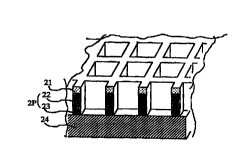
FIG. 3 is a perspective view showing the
structure of the transparent member obtained in this
example for use as a shield against electromagnetic
waves. The PET film is indicated at 21, the copper thin-
film layer at 22 and the electrolytically plated copper
thick-film layer at 23. These two layers substantially
provide a copper pattern layer 2P. Indicated at 24 is
the colored copper oxide layer.
CA 02282532 1999-08-23
-60-
Table 2
Example Opening Tt Electro- Moire Visibility
Ratio of (~) magnetic fringe
Copper wave shield
Pattern property
(~) (dB)
100 500 1
H . MHz GHz
Ex.lB 84 76.0 38 37 38 ~ Sharp image
are easily
visible
Ex.2B 81 73.4 43 43 49 o Sharp image
are easily
visible
Comp. 69 65.0 41 42 43 X Marked
Ex.lB fringes low
visibility
Comp. 49 46.8 56 51 52 o Some fringes
Ex.2B Entire screen
apears dark
A copper-deposited PET film obtained by
sputtering under the same conditions as in Example 1B was
subjected to photolithography under the following
conditions to produce an exposed lattice pattern with
square openings. The copper-deposited surface was coated
with a resist of the negative type by a roll coater-to
provide a resist layer with a thickness of 2 um. A
masking positive film bearing an image of lattice pattern
having square openings, 15 um in line width and 150 dun in
CA 02282532 1999-08-23
-61-
pitch was then held in intimate contact with the resist
layer under vacuum. The resulting sheet was thereafter
exposed to the light of an ultraviolet light source at
110 mJ/cm2. The resist was removed from the unexposed
portion (lattice pattern image) with a developer,
followed by washing with water.
Next, the copper-deposited portion of the
exposed lattice pattern having square openings was
electrolytically plated with copper to form a thick film
of copper, using phosphorus-containing copper as the
anode, the pattern as the cathode and an aqueous solution
of copper sulfate and sulfuric acid in mixture as the
plating bath, under the conditions of a bath temperature
of 23° C, a cathode current density of 1.7 A/dm2 and a
plating rate of 0.3 ~zm/min. The PET film thus plated was
thoroughly washed with water and dried. Finally, the
remaining resist film was removed from the exposed
portions (lattice opening image portions) with an aqueous
solution of sodium hydroxide (5~ in concentration),
followed by washing with water and drying. The copper
plating was 1 dun in thickness.
Subsequently, the PET film having the copper
CA 02282532 1999-08-23
-62-
plating pattern and the copper-deposited layer was etched
under the following conditions over the entire surface
thereof. The PET film was fixedly placed in the
container of an etching apparatus, and immersed in a
hydrogen peroxide-sulfuric acid etchant at 20° C with
movement to etch away the copper-deposited portions of
lattice opening image portions corresponding to the
exposed portions. The etching was thus effected for 20
seconds and immediately discontinued upon removal of the
copper-deposited portions, followed by washing with water
and drying. The copper pattern with square openings thus
obtained had a line width of 15 ~.im which was the same as
that of the pattern image on the masking positive film,
hence a 1:1 reproduction. The pattern layer had a total
thickness of 1 pnn. Although the copper plating pattern
is also etched at the same time, the result described
indicates that copper-deposited layer in the lattice
opening image portions is etched away in preference, and
that the copper plating pattern remains substantially
unetched (with no side etching). _ -
The PET film having the resulting copper
pattern was then held in contact with a sulfiding bath at
CA 02282532 1999-08-23
-63-
40° C for 60 seconds, the bath being prepared by adding
quick lime, casein and potassium sulfide to sulfur
serving as the main component and dissolving the mixture
in distilled water. The film was thereafter immediately
withdrawn from the bath, washed with water and dried.
The pattern was colored black, and the color was vivider
and darker than in Example 1B. The sheet obtained was
measured as to the same items as in Example 1B, with the
results given in Table 2.
C~parative Examn 1B
A lattice pattern of copper having square
openings was formed on a PET film under the same
conditions as in Example 2B except that the masking
positive film used had an image of the lattice pattern,
30 um in line width and 180 um in pitch. The copper
pattern obtained was 29 dun in line width and 1 ~.un in
overall thickness. Table 2 shows the other measurements
obtained.
A lattice pattern of copper having'square
openings was formed on a PET film under the same
conditions as in Example 2B except that the masking
CA 02282532 1999-08-23
-64-
positive film used had an image of the lattice pattern,
30 dun in line width and 100 dun in pitch. The copper
pattern obtained was 29 ~.im in line width and 1 dun in
overall thickness. Table 2 shows the other measurements
obtained.
E~~le 1C
The transparent sheet used was a biaxially
oriented polyethylene terephthalate film (hereinafter
referred to as "PET film"), 125 ~zm in thickness, 400 x
1000 mm in size and 90~ in Tt. The PET film was first
pretreated over one surface thereof by glow discharge.
The pretreated PET film was disposed as opposed to ITO
(target) within the vacuum container of a magnetron
sputtering apparatus, and the ITO was sputtered under the
following conditions to deposit a thin ITO film on the
entire surface of the film.
* Sputtering operation pressure....a vacuum of 2 x 10⁻³
torr obtained by replacing the air in the vacuum
container with argon gas containing 4.5~ of oxygen
* Sputtering temperature....90° C '
* Sputtering time...........4 seconds
The ITO thin-film layer thus formed by sputter
CA 02282532 2003-05-05
._ ~j y
deposition was 200 I~ in thickness, 400 S2/Ct in surface
resistivity and 88.9 in Tt.
Next, the surface of the ITO thin film was
coated with a photoresist of the positive type by a roll
coater to a thickness of ~? ~zm. fhe r:oating was then
irradiated with ultraviolet rays at an intensity of 1.30
mJ/cm2, with a masking negative film held in intimate
contact with the coating surface, the masking film
bearing an image of lattice pattern having square
openings, 15 ~zm in tine width anci 1~(~ ~Zm in pit~c:h. The
irradiated pattern portion corresponding to the pattern
image was developed f'or r:-em~val .
Accordingly, the resist in the portions
corresponding to the opening image portions remained
masked. The resulting film will hereinafter be referred
to as "ITO pattern PET film."'
Subsequently, the 1T0 pattern PET film was
immersed first in a palladium electroless plating bath
(product of Nikko Metal Plating Co., Ltd., Product No.
CG-535A, 3 to 3. 5 ire pH) at, room temperature 'fo~:~ 1
minute, thoroughly washed, and then immersed in a nickel
electroless plating bath (product ref Ni.kko Metal Plating
CA 02282532 1999-08-23
-66-
Co., Ltd., Product No. NICOM N, 4.5 to 5 in pH) at 70° C
for 5 minutes to form a nickel layer.
The palladium thus applied and the nickel layer
thus formed provide a ground layer (in this case, 0.2 dun
in thickness) for the electrolytic plating of copper to
be performed subsequently. The presence of the ground
layer permits the ITO pattern layer to bond to the copper
plating thick-film layer to be formed, whereby a copper
pattern of improved strength will be provided.
Accordingly, the provision of the ground layer
is an example of pretreatment which is to be performed
when the conductive transparent thin-film layer 32 to be
formed over the entire area is formed from ITO as the
lower layer. If the thin-film layer is prepared from a
material other than ITO, a different pretreatment (which
is not always conducted, or a different method may be
resorted to) will be performed.
The resulting PET film having the ground layer
on ITO pattern layer was then immersed in a plating bath
wherein an aqueous solution of mixture of copper sulfate
and sulfuric acid served as the cathode, with the ITO
pattern layer serving as the anode, for electrolytic
CA 02282532 2003-05-05
_,. ~ '~
plating ~2 Aldm~ in cathode currerut density, and 0.28
um/mi.n in plating rate) at room temperature. The copper
deposited by the plating was 1.1 ~~m an thickness. The
film thus obtained will hereinafter be referred to as the
"copper plating pattern PET film.w'
Next, the resist film remaining in the pattern
opening portions of the copper p:~.~~ti.r~g pattern PET film
was dissolved with acetone for removal, whereby a lattice
copper pattern with square c:>peninc~s was formed as an
upper.-layer on the ITS conductive transparent thin-film
layer provided as a lawer layer over the entire area of
the PET film. The pattern obtained was 14 pm in line
width. Table 3 shows other measui:ements as to
electromagnetic waved shield properties, Tt and mo ue
fringes.
Incidentally, the* openz.ng ratio was calculated
from Equation 1.
CA 02282532 2003-05-05
_~~_
Tsbl.e
3
Ele ITC> thinTt Shield MQire Cpexi-
Cu propeerties
pattern
line widthfilm ~'~;~~.~~c~a.t fringe ing
~
Camp. /pitch '~ 10~) 500 1.000 ratio
Ex. S~I~) a _._..~~ ~ ~"~ ..~ L~L
.
Ex. 141150 Lc~~aer '73.0ail ~0 52 cps 82.2
1C
la~re~- t
15/100 L7pper 02.058 57 56 " 72.2
layer.
15/150 " 72 a3 .~2 54 "' 81.
"? 0
Ex.
3C
15/200 " 7~a.950 ~0 54 " 85.6
15/250 " 77.347 49 56 " 88.3
---___ ~_____,~__________________________________________.~_~.___
15/100 ~ 6'S.'~0 48 49 " 72
n .2
151150 " .7:1.443 43 49 " 81.0
C. Ex. 1C
15/200 " 7?.040 40 45 " 85.6
15/250 " '79.93~ f7 42 " 88.3
C. Fx. 2C No Yes 89.410 3 2 " 100
C. F~. 3C 29.9/180Lc7wer F0.2~'7 66 &9 x X9.4
la er ... ~
CA 02282532 2003-05-05
~._~g_
The PET film having the square lattice copper
pattern and prepared in Example 1~: was oxidized under the
following conditions to color the copper surface of the
pattern to form a blackish brown crolored layer 3.
The PET film was immersed in its entirety in a
bath which was <~n aqueous solutioru obtained by dissolving
a mixture of sodium hydroxide and sodium chlorite in
water and which was heated to ~~0° ~, then withdrawn
from the bath, washed with water and dried. The copper
pattern surface was oxidized to a blackish brown copper
oxide layer. This ~:o.~.ored layer eras 0.8 ~.~m in thickness.
The resulting sheet and the sheet obtained in Example 1
were each attached to a PDP in suspension, and images on
.the screen were viewed through the sheet. Consequently
the sheet of the present example made the viewer feel at
ease the moment when the screen became visible, giving no
feeling of visual fatigue even if the screen was watched
further for a prolonged period cyf time.
No differences were found between the sheet of
this example and that of Example I with respect to other
properties, i.e., electromagnetic wave shield properties,
CA 02282532 2003-05-05
7()_
Tt and moire fring~,s .
FTG. 6 shows the structure obtained in Example
1 as well as in Example 2. T.ndicated at 31 is a PET
film, at 32 a transparent TTO thin-film layer formed as a
lower layer over the entire surface <af the film, at :33 a
copper plating layer formed by electrolytic plating, and
at 34 a blackish colored Layer of copper oxide.
Four pieces of the same PET film as used in
Example 1C were prepared and simi.Larly pretreated by glow
discharge. Each piece of PET film was disposed as
opposed to a copper target within them vacuum container of
a magnetron sputtering apparatus, and the air in the
container was completely replaced by argon gas to obtain
a vacuum of 2 x 10~' torn lJnder this operation. pressure
and with application of electric power of 9 kW (DC), the
copper was deposited ran the film wtaile causing the film
to travel at a rate of 1 mlmin. This procedure was
repeated three times to deposit a copper thin-film layer
having a thickness of 0 . 12 ~n (~() . C~1 ) .
A portion of each piece of film was cut off and
bent through 180 deg for testing, but the thin-film layer
CA 02282532 1999-08-23
-71-
was unlikely to peel off.
Next, the four pieces of PET film thus obtained
were photolithographically treated over the surface of
the copper thin film to form lattice patterns having
square openings and different in opening ratio. More
specifically, the thin film surface of each film piece
was coated with a positive photoresist (photodecomposable
type) to a thickness of 2 um. Masking negative films,
all 15 um in line width but different in pitch, i.e., 100
um, 150 um, 200 dun and 250 dun, respectively, in pitch
were prepared, and held in intimate contact with the
coating surfaces of the respective film pieces under
vacuum, followed by irradiation with an ultraviolet light
source at 110 mJ/cmz: The resist of the exposed pattern
portion of each film piece was developed for removal by
dissolving (with the resist remaining in intimate contact
with the pattern opening portions).
Subsequently, the copper thin-film layer of the
square lattice pattern formed on each piece of PET film
obtained as above was electrolytically plated with copper
under the following conditions to superpose a copper
thick layer on the thin-film layer and form a copper
CA 02282532 1999-08-23
-72-
pattern. Finally the resist film remaining in the
pattern opening portions was removed by dissolving. With
the pattern serving as the cathode, and with an aqueous
solution of mixture of copper sulfate and sulfuric acid
used as the plating bath and serving as the anode, the
thin layer was electrolytically plated at a bath
temperature of 23° C, current density of 1.7 A/dm2 and
plating rate of 0.3 um/min. The four film pieces thus
treated were all 2.5 um in the thickness of the copper
pattern resulting from the electrolytic plating.
Each of the four pieces of PET film having the
copper pattern on the copper thin film was subsequently
chemically etched under the following conditions to
remove the copper thin-film layer from the pattern
opening portions by dissolving. The PET film in its
entirety was placed in position within an etching
apparatus and held in contact with a hydrogen
peroxide/sulfuric acid etchant at 20° C for 30 seconds.
The copper thin film was removed from the pattern opening
portions by dissolving, whereupon the etching operation
was discontinued, followed by washing with water and
drying. The film pieces thus obtained were. all 2.41
CA 02282532 2003-05-05
"..~~a_
(~0.01) um in the thickness of the resulting copper
pattern. This 'thickness is not substantially different
from the thickness (2,5 um) before the etching. This is
thought attributable to the followinr~. The copper
pattern portion is etched simultaneously with the copper
thin film of the pattern opening portions, whereas there
is a great difference between the two in thickness, and
there occurs a difference between the two in the quality
of film, with the result that the copper thin film is
etched in preference.
The copper pattern was smaller than the one
obtained by the process of examples 1. in the diminution of
the line width and was reproduced in the ratio c>f 1:1.
Next, quick lime, casein and potassium sulfide were
admixed with sulfur serving as the main component, and
the mixture was dissolved i,n distill.ed water. The copper
pattern surface was held in r_ontact with the solution
serving as a sul.fiding bath at ~0° C far about 6c~ seconds,
then washed with waiters and da:ied. The surface was
colored black, and the color was darker and more vivid
than that of the copper oxide layer of Example ~C.
Next, ITU was sputtered to form a coating over
CA 02282532 2003-05-05
._
the entire surface of the colored copper pattern of each
piece of PET film having the copper pattern thus colored.
The sputtering operation was conducted under the same
conditions as in Example lc except t~raat the sputtering
time was 8 seconds. The ITO film deposited by sputtering
was 410 ~ in thickness and X00 ~/~ in surface
resistivity.
Measurement was made of the four pieces of the
films obtained with respect to the electromagnetic wave
shield properties, Tt and moue fringe relative to the
line width/pitch of the copper pataern formed. Table 3
shows the results.
Comp,~ra~v~ Exam~le_~
Four pieces of PET film were prepared which had
different syare copper patterns by forming the copper
pattern on each piece under exact:x.y the same conditions
as in Example 3C with the exception of forming no ITO
thin-film layer. Each of the f~.L~rw pieces obtained was
checked in the same manner as in Example 3C, with the
results given in Table
The same I~ET film as Cased in Example 1.C was
CA 02282532 2003-05-05
_'~ rJ-
pretreated similarly by glow dlscha:r<~e, and ITO was
deposited on the entire pretreated surface by sputtering
under the same conditions as in Example 3C to form an ITO
thin--film layer having t:he same thlc~.ness. The PET film
obtained with the IT0 transparent thin-film layer only
forrAed thereon was checked in the same manner as in
Example 3C* Table 3 shawl the resurlts.
The procedure of Example 1C was performed to
form an ITO thin-film layer over the entire surface of a
PET film and a lattice copper pattern on the thin-film
layer. under the same conditions a~~ ira Example 1C with the
exception of using a masking negative film having an
image of square lattice pattern which was 30 um in line
width and 180 ~.im in piteh* The measurements obtained of
the resulting sheet in the same manner as in Example 1C
were shown in Table 3, which reveals moue fringes
occurred.
Table 3 shows that exceedingly higher shield
effectiveness against electromagnetic waves is produced
by the combination of the copper pattern and th~~ ITO thin
film than when one of these layers is singly provided.
CA 02282532 1999-08-23
-7 6-
Furthermore, synergistic effectiveness is available
especially at electromagnetic wavelengths higher than 100
MHz. This is a surprising result.
With respect to the balance between the
transparency and the shield properties, when the
transparency is increased, the corresponding diminution
in the wave shield properties is small. This indicates
that the transparency can be increased without impairing
the shield properties, which is a feature to be highly
evaluated.
The present invention which provides the shield
transparent members of the foregoing construction has the
following advantages.
First Aspect of the Invention
The conductive reticular pattern of copper is
formed over the transparent substrate with a thin-film
layer of copper (or an alloy thereof) which is interposed
therebetween and formed directly by sputtering or like
technique, so that the pattern is bonded to the substrate
with a high strength. The member is therefore resistant
to bending or flexure, retaining the pattern against
separation even when used at high temperatures or high
CA 02282532 1999-08-23
_77_
humidities for a prolonged period of time.
Since the conductive copper pattern is directly
formed as stated above without using adhesive or the like
unlike the conventionally practice, the transparency
remains free of impairment that would result from the use
of such agent.
The electric resistivity of the conductive
pattern required for giving high shield properties is in
a narrower range, while copper is plated to a greater
thickness. The member therefore exhibits electromagnetic
wave shield effectiveness and has high transparency.
The shield transparent member of the invention
can be prepared by the process according to Item 9, which
involves no likelihood of side etching the pattern,
assuring ease of fabrication and achieving a high yield.
The surface layer of the conductive reticular
pattern can be colored brown to black with a copper oxide
or copper sulfide. The presence of the colored layer
leads to ease of viewing and diminishes visual fatigue
even if the device equipped with the member is watched
for a prolonged period of time.
Second Aspect of the Invention
CA 02282532 2003-05-05
..,.
The member of the :invention has the s~:ructure
described, hence the following advantages.
The transparent member of the invention for use
as a shield against electromagnetic waves has h_egh shield
properties and transparency and is further given
characteristics to obviate or dl..minish the occurrence of
moire fringes conventional.l.y experienced. The reticular
copper pattern has a brown to black colored surface,
which ensures improved vi.sibil.it~r.
Because of these characteristics, the
transparent member, when used as installed at the front
side of screen of tree PDP or the like, fully blocks the
electromagnetic waves emitted by the PDP or like device
or those to be received from autside, rendering the
screen images visible distinctly and c~omfarta:bly.
The shield transparent member is usable also
for CRT and other electronic infarmati_on devices besides
PDP, rendering the interior erf the device. visible and
blocking the electromagnetic waves emitted by the device
or those conversely received from other devise to prevent
the waves from causing an err~oneou~; operation.
Third Aspect of the Invention
CA 02282532 2003-05-05
_79_
A greater improvement is made in the effect to
block electromagnetic waves than where the component
layers are each singly provided the copper pattern only,
or conductive transparent thin-~f.ilm ~.ayer onlya , and a
synergistic improvement iv achierred especially in a high
electromagnetic wavelength region.
It has become ,possible tar give improved
transparency without ~.mpairing the shield effectiveness.
This overthrows an antinomic relationship generally
existing between the two propert:i~3s.
The brown to black colored layer provided over
the surface of the reticula r coppr.r pattern affords
visibility. Further the mo ue fringes occurring
especially in the case of lattice copper patterns having
square or rectangular openings cara be eliminated or
diminished.
Because of these advantages described,, the
transparent member finds wider app:>lication for use as a
shield against electramagnetic waves for PDP, CRT and
other electronic devices which emit, electromagnetic
waves.