Note: Descriptions are shown in the official language in which they were submitted.
CA 02282776 2003-10-29
- 1 -
METHOD AND APPARATUS FOR HIGH SPEED
ANALOG TO DIGITAL CONVERSION
Field of Invention
This invention relates to analog to digital converters. In particular, this
invention relates to a method and apparatus for high speed, high definition
analog to digital
conversion of a video signal for use in telecine transfer and other video
conversion processes.
Background of the Invention
Telecine transfer is a process by which a cinematographic film is transferred
to
video. A telecine apparatus scans a negative or print of a cinematographic
film and produces
an analog video signal comprising a sequence of values representing the
brightness and
colour of each image position in the scan. An analog-to-digital converter is
used to digitize
the analog video signal for storage on a media such as magnetic tape or video
disc.
Existing telecine systems represent a trade-off between speed and resolution.
When the analog signal is conwerted to a digital signal, the quantization
level of the analog to
digital converter (ADC) determines the transfer speed and the resultant
resolution of the
digital image. For example, an 8 bit ADC digitizes an analog signal at a
higher rate than a 12
bit ADC but provides significantly lower resolution.
This balance becomes particularly important in the case of high definition
video, which requires a relatively higher quantization resolution in order to
accommodate the
increased resolution of the image. In prior art analog to digital converters
higher resolution
can only be achieved at the expense of the transfer rate.
Some prior art systems have combined fine and coarse resolution analog-to-
digital converters in an attempt to increase the resolution of the digitized
signal without
substantially reducing the conversion rate.
For example, U.S. Patent No. 5,053,771 issued on October 1, 1991 to
McDermott, discloses an analog-to-digital converter that utilizes an input
signal range
selection device to select segments of the input signal for digitization using
a finer resolution
CA 02282776 2003-10-29
-2-
converter, based on the asymmetric distribution of image information in the
analog signal.
Setup parameters are stored during a "pre-scan" operation which selects those
segments of
each scene that require higher resolution scanning, and during the transfer
process these
parameters are used to control the conversion of selected segments of each
scene by
switching between coarse and fine resolution ADC's.
This technique effectively pre-scans the film to determine which segments of
the scene exposure sequence require a finer quantization to preserve the
resolution of the
image, and uses this information to control the quantization resolution during
actual
digitization. However, pre-scanning the film is a time consuming step, and the
need to isolate
scene segments for fine resolution conversion and control digitization using a
prearranged
sequence of control signals complicates the converter considerably.
It would accordingly be advantageous to provide an analog to digital converter
which provides the high definition of a fine resolution ADC without
sacrificing the speed of
the conversion or introducing additional steps into the conversion process.
Summary of the Invention
The present invention provides a method and apparatus for converting an
analog signal to a digital signal, utilizing an analog to digital converter
which provides a high
resolution video image suitable for high definition applications at a
conversion rate
comparable to that of a lower resolution ADC.
The invention accomplishes this by providing an analog to digital converter
comprising a diplexer filter which utilizes a fine resolution ADC to digitize
the low band
component of the analog video signal, and a coarse resolution ADC to digitize
the full
spectrum of the analog video signal. The coarse resolution signal is
subtracted from the fine
resolution signal to create a summed signal that includes the difference
between the low band
components of the respective ADC outputs. The summed signal is filtered
through a low
pass digital filter to filter out the high band components and pass the
quantization error. The
coarse resolution signal is delayed as necessary to match any delay in the
filter, and the
quantization error is added to the output of the coarse resolution ADC to
effectively restore
CA 02282776 1999-09-17
-3-
the 12 bit resolution of the low band component. The output is a digital
signal having a
resolution suitable for high definition applications such as HDTV.
The present invention thus provides a method of converting an analog signal
to a digital signal, comprising the steps of digitizing a low band component
of the analog
signal to produce a fine resolution signal, digitizing high and low band
components of the
analog signal to produce a coarse resolution signal, subtracting the coarse
resolution signal
from the fine resolution signal to produce a summed signal containing a
difference between
low band components of the fine resolution signal and the coarse resolution
signal, filtering
the summed signal through a low pass digital filter to eliminate high band
components of the
summed signal and pass the difference between low band components, and summing
the
filtered signal with the coarse resolution signal to produce a digital output
signal.
The present invention further provides a converter for converting an analog
signal to a digital signal, comprising a fine resolution analog to digital
converter for digitizing
a low band component of the analog signal and producing a fine resolution
digital signal, a
coarse resolution analog to digital converter for digitizing high and low band
components of
the analog signal and producing a coarse resolution digital signal, a
processor for subtracting
the coarse resolution signal from the fine resolution signal to produce a
summed signal
containing a difference between low band components of the coarse resolution
signal and the
fme resolution signal, a low pass digital filter for eliminating a high band
component of the
summed signal and passing the difference between low band components, and a
processor for
adding the filtered signal to the coarse resolution signal to produce a
digital output signal.
In a preferred embodiment of the invention the fine resolution ADC samples at
a lower sampling rate than the coarse resolution ADC and the fine resolution
signal is
upsampled to the sampling rate of the coarse resolution signal before summing.
In a further preferred embodiment a delay is provided to delay the fine
resolution signal to match any delay in the low pass digital filter before
summing the
quantization error and the coarse resolution signal.
CA 02282776 2003-10-29
-4-
Brief Description of the Drawings
In drawings which illustrate by way of example only a preferred embodiment
of the invention,
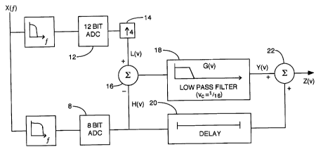
Figure 1 is a schematic diagram illustrating an analog to digital filter
according to the invention.
Detailed Description of the Invention
The invention digitizes an analog input signal X(f) representing the film
density of each image position. scanned in a scene from a cinematographic film
or negative,
for example by a scanner in a telecine apparatus. The film density information
in the analog
signal is related to corresponding values for conversion into a digital
signal, as is described in
U.S. Patent No. 5,053,771 issued to McDermott on October l, 1991. The
invention may be
used to digitize any analog signal, and is particularly advantageously used in
the digitization
of a video signal including a signal generated by an imaging orthicon or
stored on magnetic
tape or other media.
According to the invention, the analog input signal X(f) is processed in
parallel by a coarse resolution ADC 8 and a fine resolution ADC 12.
The coarse resolution ADC 8 digitizes the full spectrum of the input signal
X(f), and outputs a coarse resolution signal containing both low and high band
components.
The fine resolution ADC 12 digitizes only the low band component of the input
signal X(f)
(for example, up to 20 MHz).
In the embodiment illustrated the coarse resolution ADC 8 outputs a coarse
resolution signal at a sampling rate of 160 MSamples/s and the fine resolution
ADC 12
outputs a fine resolution signal at a sampling rate of 40 MSamples/s. In the
preferred
embodiment illustrated the sampling rate of the coarse resolution ADC 8 is an
integral
multiple of the sampling rate of the fine resolution ADC 12, and the fine
resolution signal is
upsampled through an interpolator 14 by a factor of four, to match the 160
MSamples/s
sampling rate of the coarse resolution signal.
CA 02282776 1999-09-17
-5-
The fine resolution ADC 12 outputs a fine resolution signal which is
upsampled by the interpolator 14 to produce a fine resolution signal L(v)
consisting of the
primary spectrum Lo(v) and the image spectra L,(v):
( 1 ) L(v) = Lo(v) + L,(v)
where v is the normalized frequency referred to the sampling rate of the
coarse resolution
ADC 8.
The coarse resolution ADC 8 outputs a coarse resolution signal H(v), which
consists of a low band component HL(v) and a high band component HH(v):
(2) H(v) = H~(v) + H,,(v)
H~(v) contains the same low band component present in the primary spectrum
Lo(v) of the fine resolution signal. However, H~(v) is quantized to 8 bits
while Lo(v) is
quantized to 12 bits. The difference between H~(v) and Lo(v) can be considered
a
quantization error s (v), such that
(3) H~(v) = Lo(v) + s (v)
Substituting equation (3) into equation (2), the coarse resolution output H(v)
can be expressed as
(4) H(v) = Lo(v) + E(v) + H,,(v).
The fine resolution signal L(v) and the coarse resolution signal H(v) are
processed by a processor 16 comprising an inverter/adder, which subtracts the
coarse
resolution signal H(v) from the fine resolution signal L(v) by generating a
complement of
H(v) and summing the complementary signal - H(v) with the fine resolution
signal L(v) to
produce a summed signal L(v) - H(v). The summed signal L(v) - H(v) consists of
the high
band components of L,(v) and -H,,(v), and a quantization error -e(v):
(5) L(v) - H(v) = Lo(v) + L,(v) - (Lo(v) + s(v) + H"(v))
or
CA 02282776 1999-09-17
-6-
(6) L(v) - H(v) = Lo(v) + L,(v) - Lo(v) - s(v) - H"(v)
or
(7) L(v) - H(v) = L,(v) - E(v) - H"(v)
The summed signal L(v) - H(v) is processed though a low pass digital filter
18,
in the preferred embodiment illustrated sampling at 160 MSamples/s and having
a cutoff
frequency v~ of approximately 10 MSamples/s. The filter 18 eliminates the high
band
components L,(v) and -H"(v) and passes the low band quantization error -s(v),
outputting a
signal Y(v) represented by
(8) Y(v) = G(v) [ L(v) - H(v) ]
where G(v) is the frequency response of the low pass filter 18.
Substituting equation (7) into equation (8), yields
(9) Y(v) = G(v) [ L,(v) - s(v) - H"(v) ]
Since at high frequencies G(v) - 0, the low pass filter 18 eliminates (L,(v) -
H"(v)), the high band component of the summed signal, and passes the
quantization error -
s(v). The coarse resolution signal H(v) is delayed by a digital delay 20 as
necessary to match
any delay in the summed signal L(v) - H(v) caused by the filter 18, and adder
22 sums the
output Y(v) of the filter 18, which is essentially the quantization error -
s(v), with the coarse
resolution signal H(v) to produce the digital output signal Z(v).
Summing the quantization error -E(v) with the coarse resolution signal H~(v)
produces H,,(v) - E(v), which is essentially the desired fine resolution low
band output signal
Lo(v) (see equation 3). This can be shown as follows:
( 10) Z(v) = Y(v) + H(v)
Substituting equations (4) and (9) into equation ( 10) yields
(11) Z(v) = G(v) [ L,(v) - s (v) - H"(v) ] + Lo(v) + E(v) + H"(v)
CA 02282776 1999-09-17
-7_
or
(12) Z(v) = G(v) L,(v) - G(v) E(v) - G(v) H"(v) + Lo(v) + e(v) + H,,(v)
or
(13) Z(v) = Lo(v) + HH(v) [ 1 - G(v) ] + s(v) [1 - G(v) ) + L,(v) G(v)
At the low frequencies passed by the low pass filter 18, G(v) = 1 and L,(v) =
0
(by definition). Thus, the high band component H"(v) and the quantization
error s(v) are
eliminated, leaving
(14) Z(v) - Lo(v)
In effect, summing the coarse resolution signal complement -H~(v) with the
fine resolution signal Lo(v) generates a quantization error s(v) (or - E(v))
representing the
difference between the low frequency components of the coarse and fine
resolution signals
H(v) and L(v). At the low frequencies of the low pass filter 18 the
quantization error -s(v)
passes through the filter 18 and is recombined with H~(v) at the filter output
to reconstitute
the fine resolution low band output Lo(v). At high frequencies the output of
the low pass
filter 18 is essentially zero, so the high band component of Z(v) is H"(v)
directly from the
coarse resolution ADC 8. By using a fine resolution ADC 12 to quantize only
the low band
component of the analog input signal, the high speed of the transfer process
is retained
without detracting from the resolution of the output signal.
The fine resolution ADC 12 outputs a high resolution, low bandwidth (i.e. low
noise but visually soft) signal, while the coarse resolution ADC 8 outputs a
low resolution,
high bandwidth (i.e. noisy but visually sharp) signal. Combining the outputs
of the coarse
and fine ADC's 8, 12 according to the invention optimizes the use of the ADC's
8, 12 in the
frequency range most appropriate for each particular ADC 8 or 12. At low
frequencies the
output signal Z(v) is derived completely from the fine resolution ADC 12, and
at high
frequencies the output signal Z(v) is derived completely from the coarse
resolution ADC 8.
The characteristics of the filter 18 determine the extent to which each ADC 8
or 12 contributes to the output signal Z(v) in the transition region, i.e.
where 0 < ~ G(v) ~ < 1,
CA 02282776 1999-09-17
_g_
within which both ADC's 8 and 12 contribute to the output signal Z(v). In the
transition
region of the filter 18 the effective number of bits ranges from 12 bits
within the passband of
the filter 18, through 1 l, 10 and 9 bits within the transition region, to 8
bits in the stop band
of the filter 18. The converter of the invention thus provides a smooth
transition between high
resolution at low frequencies and low resolution at high frequencies.
A preferred embodiment of the invention having been thus described by way
of example only, it will be apparent to those skilled in the art that certain
modifications and
adaptations may be made without departing from the scope of the invention. The
invention is
intended to include all such modifications as fall within the invention as set
out in the
appended claims.