Note: Descriptions are shown in the official language in which they were submitted.
CA 02283024 1999-09-22
PROTECTION FROM OVERHEATING OF A SWITCHING TRANSISTOR
THAT DELIVERS CURRENT TO A DAYTIME RUNNING LIGHT ON A VEHICLE
Technical Field
$ This invention relates to circuits for controlling daytime running lights on
vehicles,
and more particularly to a circuit for protecting from overheating a switching
transistor that
delivers current to a daytime running light on a vehicle.
Background of the Invention
Daytime running lights augment vehicle safety by enhancing the visibility of a
vehicle having daytime running lights. Thus, daytime running lights are
becoming a more
common feature on vehicles. Because of the recognized importance of daytime
running
lights on vehicles, Canada has legislated to require daytime running lights on
vehicles that
are sold in Canada.
1$ In daytime running lights on a vehicle, a high-power output switching
transistor
delivers current to a high wattage daytime running light bulb filament on the
vehicle.
Refernng to Fig. 1, a high-power MOSFET (Metal Oxide Semiconductor Field
Effect
Transistor) 102 is used to deliver current from a power source 104 to the
filament of a
daytime running light 106. The intensity (and thus the brightness) of the
daytime running
light is determined by the duty cycle of a switched DC voltage applied to the
gate of the
MOSFET 102.
Note, that a high power BJT (Bipolar Junction Transistor) may be used instead
of the
MOSFET 102 to deliver current from the power source 104 to the filament of the
daytime
running light 106. As would be apparent to one of ordinary skill in the art,
the present
2$ invention may be used in conjunction with a MOSFET or a BJT or any other
type of high
power switching device from the description herein. The MOSFET 102 is shown as
an
example switching device. However, a MOSFET may be preferred as the switching
device
rather than a BJT because of the higher switching speed and lower resistance
of a MOSFET
when the MOSFET is turned on.
The power source 104 is typically from a battery system of the vehicle, and
the
battery system includes a fuse which blows and open-circuits the drain of the
MOSFET 102
from the power source 104 when excessive current flows though such a fuse.
However, a
partial short load 108 may be coupled to the source of the MOSFET 102. The
partial short
CA 02283024 1999-09-22
load 108 has an impedance which is not low enough to blow the fuse of the
battery system.
Nevertheless, the impedance of the partial short load 108 may be low enough to
cause high
current to flow through the switching MOSFET 102.
Such high current flowing through the switching MOSFET 102 results in high
heat
and thus damage to the switching MOSFET 102. The damage to the switching
MOSFET
102 results in an effective resistance 110. As high current continues to flow
through the
effective resistance 110, excessive overheating and/or even a fire may result
in malfunction
of the daytime running light system and could potentially be a further hazard
to the vehicle.
Prior art protection circuits, for preventing damage to the switching
transistor 102,
control the current flowing though the switching transistor 102 by controlling
the gate
voltage if the switching transistor is a MOSFET or by controlling the base
current if the
switching transistor is a BJT (Bipolar Junction Transistor). U. S. Patent No.
4,926,283 to
Qualich, U. S. Patent No. 4,595,966 to Huber et al, U. S. Patent No. 4,750,079
to Fay et al.,
U. S. Patent No. 5,272,392 to Wong et al., U. S. Patent No. 5,390,069 to
Marshall, U. S.
Patent No. 5,438,237 to Mullins et al., and U. S. Patent No. 5,694,282 to
Yockey, teach a
protection circuit 112 which controls the current flowing through a MOSFET
output
transistor by correspondingly controlling the gate to source voltage of the
MOSFET output
transistor. U. S. Patent No. 4,360,852 to Gilmore and U. S. Patent No.
4,800,331 to Vesce et
al. teach a protection circuit 112 which controls the current flowing through
a BJT output
transistor by correspondingly controlling the base current of the BJT output
transistor.
Unfortunately, with the prior art protection circuit 112, a conductive path
still exists
from the power source 104 through the effective resistance 110 of the damaged
MOSFET
102 to the partial short load 108. Even with the prior art protection circuit
112, excessive
current may still flow through such a conductive path. Such excessive current
may cause
sufficient damage to the switching transistor 102 such that the daytime
running light
becomes inoperative. Additionally, such excessive current may cause excessive
overheating
and even a fire resulting in further hazard to the vehicle.
In addition, the prior art protection circuit 112 does not include a latching
circuit to
keep the daytime running light turned off once the switching transistor
reaches an excessive
temperature. Without the latching circuit, the daytime running light may flash
on and off as
2
CA 02283024 1999-09-22
the switching transistor alternately cools off and turns back on and then
heats up and turns
back off from the mechanism of the prior art protection circuit. Such flashing
on and off of
the daytime running light may be a traffic hazard on the road and also causes
further
degradation of the switching transistor 102.
Summary of the Invention
Accordingly, in light of these disadvantages of the prior art protection
circuit, the
present invention is an improved mechanism for protecting from overheating a
switching
transistor that delivers current from a power source to a daytime running
light on a vehicle.
The protection circuit of the present invention open-circuits the switching
transistor from the
power source when the temperature at the switching transistor is sensed to be
above a
predetermined temperature. In this manner, the conductive path from the power
source
through.the switching transistor is open-circuited such that current cannot
continuously flow
through the switching transistor. Thus, overheating of the switching
transistor from
excessive current flow is prevented with the present invention.
Furthermore, a latching circuit in the protection circuit of the present
invenrion
maintains the switching device to be turned off once the temperature at the
switching
transistor reaches the predetermined temperature.
Generally, the present invention is a circuit for protecting a switching
transistor from
overheating. The switching transistor drives a daytime running light on a
vehicle by
delivering current from a power source to a daytime running light filament.
The circuit of
the present invention includes a sensor, such as a thermistor, operatively
coupled to the
switching transistor, for monitoring temperature at the switching transistor.
The circuit of
the present invention also includes a switching device, such as a relay
switch, operatively
coupled between the power source and the switching transistor. The switching
transistor
delivers current from the power source to the daytime running light when the
switching
device is closed. In addition, the circuit of the present invention includes a
control circuit,
operatively coupled to the sensor and the switching device, for controlling
the switching
device to open when the sensor senses that the temperature at the switching
transistor is
greater than a predetermined temperature to open-circuit the switching
transistor from the
power source.
3
CA 02283024 1999-09-22
The present invention may be used to particular advantage when the circuit of
the
present invention further includes a latching circuit for maintaining the
switching device
open once the switching device has been opened. The switching device closes
again when
the temperature at the switching transistor has returned to being lower than
the
predetermined temperature and when the power source is reapplied to the
protection circuit.
These and other features and advantages of the present invention will be
better
understood by considering the following detailed description of the invention
which is
presented with the attached drawings.
Brief Description of the Drawings
Fig. 1 shows a switching transistor for delivering power to a daytime running
light on
a vehicle and shows a protection circuit for protecting the switching
transistor from
overheating, according to the prior art;
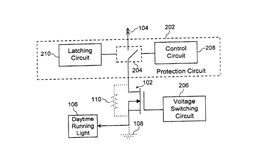
Fig. 2 shows a switching transistor for delivering power to a daytime running
light on
a vehicle and shows a block diagram of a protection circuit for protecting the
switching
transistor from overheating, according to the present invention;
Fig. 3 shows implementation of the protection circuit for protecting the
switching
transistor as shown in Fig. 2, according to one embodiment of the present
invention; and
Fig. 4 shows implementation of the protection circuit for protecting the
switching
transistor as shown in Fig. 2, according to another embodiment of the present
invention.
The figures referred to herein are drawn for clarity of illustration and are
not
necessarily drawn to scale. Elements having the same reference number in Figs.
1-4 refer to
elements having similar structure and function.
Detailed Description
Referring to Fig. 2, a protection circuit 202 of the present invention for
protecting the
switching transistor 102 from overheating includes a switching device 204
coupled between
the power source 104 and the drain of the switching transistor 102. The
switching transistor
102 delivers current from the power source 104 to the filament of the daytime
running light
106 when the switching device 204 is closed. A voltage switching circuit 206
drives the gate
of the switching transistor 102 with a switched DC voltage having a duty cycle
that
4
CA 02283024 1999-09-22
determines the power and thus intensity (i.e., the brightness) of the daytime
running light
106. The voltage switching circuit 206 may be implemented in any way known to
one of
ordinary skill in the art for switching a DC voltage. .
A sensor (not shown in Fig. 2) is coupled to the switching transistor 102 for
monitoring the temperature at the switching transistor 102. When the
temperature at the
switching transistor 102 is sensed to be greater than a predetermined
temperature, a control
circuit 208, coupled to the sensor and the switching device 204, controls the
switching
device 204 to open. When the switching device 204 opens, the drain of the
switching
transistor 102 is open-circuited from the power source 104 such that current
cannot flow
from the drain to the source of the switching transistor 102.
By thus preventing excessive current flow through the switching transistor
102, the
switching transistor 102 is prevented from further overheating due to
excessive current flow
through the effective resistance 110 of the switching transistor 102. The
effective resistance
110 results from damage to the MOSFET 102 when high current flows through the
MOSFET 102 during a reaction time of the protection circuit 202.
Additionally, the present invention includes a latching circuit 210 coupled to
the
switching device 204 for maintaining the switching device 204 open until the
temperature at
the MOSFET 102 is below the predetermined temperature and until the power
source 104 is
reapplied to the protection circuit 202. Without the latching circuit, the
switching device 204
may alternately open and close as the switching transistor alternately cools
off after the
switching device 204 is opened and heats up after the switching device 204 is
closed. Such a
repeated opening and closing of the switching device 204 leads to further
degradation of the
switching transistor 102 and to undesirable flashing on and off of the daytime
running light
which may be a traffic hazard on the road.
Thus, a latching circuit 210 is included to maintain the switching device 204
to be
opened once the temperature at the switching transistor 102 reaches a
predetermined
temperature. The switching device 204 closes again when the temperature at the
MOSFET
102 is below the predetermined temperature and when the power source 104 is
reapplied to
the protection circuit 202.
Referring to Fig. 3, an example implementation of the protection circuit 202
of Fib
5
CA 02283024 1999-09-22
is shown. The switching device 204 is comprised of a relay switch 301 which is
controlled
to open and close depending on the current flowing through a coil 302. The
relay switch 301
is coupled between the drain of the switching MOSFET 102 and a battery system
333 via a
first fuse 331. The coil 302 is coupled to the battery system 333 via a second
fuse 332 and
an ignition system 335 of the vehicle. If sufficient current flows through the
coil 302, then
the relay switch 301 is closed; otherwise, the relay switch 301 is opened.
The sensor for monitoring the temperature at the switching transistor 102 is a
thermistor 304. The thermistor 304 is disposed to form a temperature-
conductive path with
the switching transistor 102. For example, the thermistor 304 may be disposed
on a heat
sink mounted to a junction of the switching transistor 102. The thermistor 304
has a
resistance that varies with temperature. The thermistor 304 is coupled as a
resistive-divider
with a first resistor 306 between a regulated voltage node 339 from a voltage
regulator 337
and a ground node 308.
The control circuit 208 of Fig. 2 is comprised of a first BJT (Bipolar
Junction
Transistor) 312 and a second BJT (Bipolar Junction Transistor) 314 in Fig. 3.
A capacitor
310 may be connected in parallel with the thermistor 304 to provide filtering
of electrical
noise that may otherwise cause inappropriate operation of the first BJT 312.
The present
invention may be practiced with or without the inclusion of the capacitor 310.
A second
resistor 316 and a third resistor 318 form a voltage divider for biasing the
base of the first
BJT 312. A fourth resistor 320 and a fifth resistor 322 form a voltage divider
for biasing the
base of the second BJT 314.
The control circuit 208, comprising the first BJT 312 and the second BJT 314
in
Fig. 3, operates in the following manner. When the temperature at the
switching transistor
102 rises, the temperature and thus the resistance of the thermistor 304
increases. As a
result, the voltage at the base and thus the collector current of the first
BJT 312 increase.
The collector of the first BJT 312 is coupled to the base of the second BJT
314 via a diode
324. Thus, when the collector current of the first BJT 312 increases, the base
current of the
second BJT 314 decreases. When the base current of the second BJT 314
decreases, the
collector current of the second BJT 314 also decreases.
When the temperature at the switching transistor 102 rises to a predetermined
6
CA 02283024 1999-09-22
temperature, the collector current of the second BJT 314 decreases to a
sufficiently low level
such that the relay switch 301 opens. Since the coil 302 is coupled to the
collector of the
second BJT 314, the current Mowing through the coil 302 is not sufficient to
close the relay
switch 301. Thus, when the temperature at the switching transistor 102 reaches
the
predetermined temperature, the power source from the battery system 333 of the
vehicle is
open-circuited from the drain of the switching MOSFET 102. In that case,
current does not
flow from the power source 333 through the switching MOSFET 102. Thus, the
present
invention thereby prevents overheating of the switching MOSFET 102 from
excessive
current flow through the effective resistance 110 of the switching MOSFET 102.
The latching circuit 210 of Fig. 2 is comprised of the first BJT 312 and a
third BJT
(Bipolar Junction Transistor) 326 in Fig. 3. A sixth resistor 328 and a
seventh resistor 330
form a voltage divider for biasing the base of the third BJT 326. The first
BJT 312 which is
an NPN BJT and the third BJT 326 which is a PNP BJT are coupled in a latching
configuration. In that configuration, the base of the first BJT 312 is coupled
to the collector
I 5 of the third BJT 326, and the base of the third BJT 326 is coupled to the
collector of the first
BJT 312.
The latching circuit 210, comprising the first BJT 312 and the third BJT 326
in
Fig. 3, operates in the following manner. When the temperature of the
switching transistor
102 rises and the resistance of the thermistor 304 increases, the voltage at
the base of the first
BJT 312 increases. The first BJT 312 turns on with more current from the
increase of its
base voltage.
The collector of the first BJT 312 is coupled to the base of the third BJT
326. Thus,
when the first NPN BJT 312 has higher collector current, the third PNP BJT 326
also turns
on with more current since the higher collector current of the first BJT 312
results in higher
base cun:ent of the third BJT 326. In turn, when the third PNP BJT 326 turns
on with higher
collector current, the first BJT 312 also turns on with more current since the
higher collector
current of the third BJT 326 results in higher base current of the first BJT
312. Thus, the
first BJT 312 and the third BJT 326 are coupled in a latching configuration
and keep each
other turned on once one of the two BJTs 312 and 326 turns on.
Since the first BJT 312 is maintained on in this manner, the second BJT 314 is
kept
7
CA 02283024 1999-09-22
turned offonce the switching transistor 102 reaches the predetermined
temperature. With
the second BJT 314 turned off, the relay switch 301 is also maintained to be
open until the
temperature at the MOSFET 102 decreases below the predetermined temperature
and until
the power source 333 is removed and reapplied to the protection circuit 202 of
the present
invention. The power source 333 may be removed and reapplied from the ignition
system
335 of the vehicle having the daytime running light 106. Alternatively, the
power source
333 may be removed and reapplied to the protection circuit 202 by
disconnecting and then
reconnecting the power source 333 via any other mechanisms known to one of
ordinary skill.
in the art.
Thus, with such a latching circuit 210, the daytime running light 106 is
maintained
off once the switching transistor 102 overheats. Thus, the traffic hazard and
the faster
degradation of the switching transistor 102, which may result when the daytime
running light
flashes on and off, are avoided with the latching circuit 210.
In this manner, the protection circuit of the present invention prevents
destruction or
degradation of the switching transistor 102 from overheating when a partial
short load 108 is
coupled to the switching transistor 102. The first fuse 331 is typically
included with the
battery system 333, and the second fuse 332 is typically included with the
ignition system
335 of the vehicle. These fuses 331 and 332 prevent excessive current flow
through the
battery system 333. However, when a partial short load 108 is coupled to the
switching
transistor, the impedance of the partial short load 108 may not be low enough
to blow those
fuses 331 and 332.
Nevertheless, the impedance of the partial short load 108 may be low enough to
cause excessive current to flow through the switching transistor 102. Such
excessive current
flowing thmugh the MOSFET 102 may result in the effective resistance 110. If a
conductive
path from the power source 333 through the effective resistance 110 remains,
excessive heat
or even a fire may be generated resulting in malfunction of the daytime
running light system.
By open-circuiting the switching transistor 102 from the power source 333 when
overheating is detected, current is cut-off from the switching transistor 102
immediately
upon detection of overheating. In contrast to the prior art protection circuit
of Fig. 1, current
does not continue to flow through the effective resistance 110 upon damage to
the MOSFET
CA 02283024 1999-09-22
102. The prior art protection circuit of Fig. 1 controls the gate voltage of
the switching
transistor 102. Thus, in the prior art, current may continue to flow through
the effective
resistance 110 upon damage to MOSFET 102 since a conductive path from the
power source
through the effective resistance 110 remains.
Referring to Fig. 4, an alternative implementation of the protection circuit
202 of Fig.
2 includes the control circuit 208 having a comparator 402. Referring to Fig.
4, a first
resistor 404 and a second resistor 405 with a first coupling capacitor 407 set
a reference
voltage at a positive node 410 of the comparator 402. A second coupling
capacitor 412 is
coupled between the positive node 410 and a negative node 414 of the
comparator 402. The
thenmistor 304 is coupled to the negative node 414 of the comparator 402
through a third
resistor 416. A bias voltage at the negative node 414 of the comparator 402 is
set by the
third resistor 416 and a fourth resistor 418.
Referring to Fig. 4, the control circuit 208 also includes a first BJT
(Bipolar Junction
Transistor) 420 having its collector coupled to the coil 302 of the switching
device 204. The
first BJT has an emitter coupled to ground 308 via a first diode 422. The base
of the first
BJT 420 is coupled to an output node 424 of the comparator 402 via a second
diode 426.
The base of the first BJT 420 is also coupled to ground via a fifth resistor
428. The first
resistor 404, a sixth resistor 406, and a seventh resistor 408 set a bias
voltage at the output
node 424 of the comparator 402. The sixth resistor 406 also forms a feedback
circuit
between the positive node 410 and the output node 424 of the comparator 402.
The control circuit 208, as implemented in Fig. 4 with the comparator 402 and
the
first BJT 420, operates in the following manner. A reference voltage is set at
the positive
node 410 of the comparator 402 by the voltage divider comprising the first
resistor 404 and
the second resistor 405 coupled between the regulated voltage node 339 and the
ground node
308. Initially, when the temperature at the thermistor 304 is low, the voltage
at the output
node 424 of the comparator 402 is high.
When the temperature at the switching transistor 102 rises (such as when the
partial
short load 108 is coupled to the switching transistor 102 for example), the
temperature and
resistance of the thermistor 304 increase. As the resistance of the thermistor
304 increases,
the voltage at the negative node 414 of the comparator 402 increases. As the
resistance of
9
CA 02283024 1999-09-22
the thermistor 304 increases, eventually, the voltage at the negative node 414
exceeds the
reference voltage set at the positive node 410 of the comparator 402. In that
event, the
voltage at the output node 424 of the comparator 402 decreases dramatically to
a low
voltage. As a result, the base voltage of the first BJT 420 decreases to a low
voltage, and the
collector current through the first BJT 420 decreases.
When the temperature at the switching transistor 102 reaches a predetermined
temperature, the collector current of the first BJT 420 decreases to a
sufficiently low level
such that the relay switch 301 opens. In that case, the current flowing
through the coil 302 is
not sufficient to close the relay switch 301. Thus, when the temperature at
the switching
transistor 102 reaches the predetermined temperature, the power source 333 is
open-circuited
from the drain of the switching MOSFET 102. In that case, current cannot flow
from the
power source 333 through the effective resistance 110 of the switching MOSFET
102. Thus,
the present invention thereby prevents further overheating of the switching
MOSFET 102
from continuous current flow after initial damage to the MOSFET 102.
Referring to Fig. 4, the alternative implementation of the protection circuit
also
includes a latching circuit comprised of the sixth resistor 406 and the first
BJT 420. The
sixth resistor 406 forms a feedback circuit in the feedback path from the
positive input node
410 to the output node 424 of the comparator 402. When the temperature at the
thermistor
304 has reached the predetermined temperature resulting in low voltage at the
output node
424, the sixth resistor 406 is effectively in parallel connection with the
first resistor 404.
With such a feedback circuit, the positive input node 410 of the comparator
402 is
maintained to have a low voltage. Thus, even if the temperature at the
thermistor 304
decreases back down, the voltage at the negative input 414 remains higher than
the low
voltage maintained at the positive input node 410. Thus, the output node 304
is latched to
remain in a low voltage, and the relay switch 301 is maintained to be open.
This latching of the relay switch 301 may be reset when the temperature at the
MOSFET 102 decreases below the predetermined temperature and by removing and
reapplying the power source 333 to the protection circuit of the present
invention. The
power source 333 may be removed and reapplied from the ignition system 335 of
the vehicle
having the daytime running light 106. Alternatively, the power source 333 may
be removed
CA 02283024 1999-09-22
and reapplied to the protection circuit 202 by disconnecting and then
reconnecting the power
source 333 via any other mechanisms known to one of ordinary skill in the art.
With such a latching circuit, the daytime running light is maintained off once
the
switching transistor 102 overheats to the predetermined temperature. Thus, the
traffic hazard
and faster degradation of the switching transistor 102, which may result when
the daytime
running light flashes on and off, are avoided with the latching circuit.
The alternative implementation of the protection circuit of Fig. 4 also
includes a
parking brake latching circuit comprised of a second BJT 430 coupled to the
first BJT 420
and to a parking brake switch 450 of a parking brake system on the vehicle
having the
daytime running light 106. An eighth resistor 432 and a ninth resistor 434
bias the base of
the second BJT 430. The collector of the second BJT 430 is coupled to the base
of the first
BJT 420 through a tenth resistor 436. The collector of the first BJT 420 is
coupled to the
base of the second BJT 430 through an eleventh resistor 438. In this manner
the first BJT
420 and the second BJT 430 are coupled in a latching configuration.
A first node of the parking brake switch 450 is coupled to the base of the
first BJT
420 via a twelfth resistor 452, a third diode 454, and a fourth diode 456. The
first node of
the parking brake switch 450 is also coupled to the regulated voltage node 339
from the
voltage regulator 337 via a thirteenth resistor 458 and the fourth diode 456.
A second node
of the parking brake 450 is coupled to the ground node 308.
Before the vehicle is started, the parking brake system is turned on such that
the
vehicle is in parked mode. When the vehicle is started, the daytime running
light 106 is
maintained to be turned off such that all of the battery power from the
battery system 333 is
used to start the vehicle. The latching configuration of the first BJT 420 and
the second BJT
430 ensures that the daytime running light 106 is maintained off when the
vehicle is in
parked mode as now described herein.
When the parking brake system is turned on, the parking brake switch 450 is
closed
to couple the base of the first BJT 420 to the ground node 308. With the base
of the first
BJT 420 coupled to the ground node 308, the first BJT 420 turns off. With the
first BJT 420
turned off, the second BJT 430 is also turned off because of the latching
configuration of the
first BJT 420 and the second BJT 430. In addition, the first BJT 420 and the
second BJT
11
CA 02283024 1999-09-22
430 continue to keep each other turned off because of the latching
configuration. Thus, the
daytime running light 106 is maintained off when the vehicle is in parked
mode.
After the vehicle has started and the parking brake system is in drive mode,
the
parking brake switch 450 is turned off (i.e., the base of the first BJT 420 is
open circuited
from the ground node 308), and the voltage at the base of the first BJT 420
charges back up.
Thus, the first BJT 420 turns on, and in turn, the second BJT 430 is also
turned on.
Subsequently, the latching configuration of the first BJT 420 and the second
BJT 430
maintains the first BJT 420 and the second BJT 430 to be turned on regardless
of the state of
the parking brake switch 450 once the vehicle has been started. The first BJT
420 and the
second BJT 430 may turn off subsequently when the temperature at the
thenmistor 304 is
above the predetermined temperature.
The foregoing is by way of example only and is not intended to be limiting.
For
example, the advantageous features of the present invention may be used in
conjunction with
any other type of switching transistor 102 aside from just the example of the
MOSFET. In
addition, any type of sensor 304 for sensing the temperature at the switching
transistor 102
may be used aside from just the example of the thermistor. Also, any type of
switching
device 204 aside from just the example of the relay switch may be used with
the present
invention. Furthermore, other implementations for the control circuit 208 and
the latching
circuit 210 as apparent to one of ordinary skill in the art may be used with
the present
invention.
Therefore, the present invention is limited only as defined in the following
claims
and equivalents thereof.
12