Note: Descriptions are shown in the official language in which they were submitted.
. CA 02283180 1999-09-02
r r, . c a n r .
r . r,
r -1-. . , . .. .,. . ,
APPARATUS A1V'D METHOD FOR PERFORMING TIMING RECOVERY
BACKGROUND OF THE INVENTION
Field of the Invention.
This invention relates in general to a timing recovery system and method,
and more particularly to a phase-locked loop timing recovery system and method
which is
highly effective in eliminating re-activation.
_Description of Related Art.
At a receiver in a typical communication system, an analog-to-digital
converter is utilized to convert a received continuous-time signal into a
discrete-time
format. One problem which is encountered in this type of system is that the
local receiver
clock and the remote transmitter clock are asynchronous. If the receiver clock
is slower
1o than the transmitter cloak, after a long enough period of time, one sample
of the received
continuous-time signal will be lost. On the other hand, if the local receiver
clock is faster
than the remote transmitter clock, after a long enough period of time, an
extra sample of
the received continuous-time signal will be obtained. Thus, the problem of
recovering the
clock signal is an important problem in many communication systems.
Recently, several high speed digital data services have become
commercially available. These high speed digital data services are known as
the
ISDN(Integral Services Digital Network) basic rate, HDSL(High Speed Digital
Subscriber Loop), HDSL2(High Speed Digital Subscriber Loop 2), ADSL(Asymmetric
Digital Subscriber Loop), and TI services.
2o In these transmission system, the transceiver needs to recover the clock
signal to provide the high speed services. In particular; a phase-locked loop
(PLL) is need
to obtain the clock signal. At the slave side(normally called Remote side,
RT), the loop
timing needed to be acquired from the received signal sent from the master
side(normally
called Central Office side, CO). The RT transmitter sends back a signal to the
CO side
with the synchronous time base acquired in its receiver phase-locked loop.
Further, some
systems use the signal carrierless AM/PM (CAP) or quadrature amplitude
modulation
(QAM) signal as the line code, which is very effective when the cable loss is
heavily
~ distorted due to skin effect of the cable and the open-ended stub, bridged
taps.
U.S. Patent 5,581,585 to Takatori et al. discloses a phase-locked loop
3o timing recovery circuit. The circuit includes a feed-forward equalizer 22,
a decision
equalizer feedback unit 24, and a phase detector 26 (Fig. 2). The input signal
received
~4MENDED SHEET
CA 02283180 1999-09-02
'a - ' ~ ..' , '~ ~ ; , ~ " , .
.,. ~ ,
-lA-
over line 12 is sampled by switch 14 using a clock signal. The signal 16
controls the
sample rate and is adjusted by automatic gain control (AGC) 20. The feed
forward
equalizer 22 adapts to the line response so that the node immediately prior to
the decision
feedback equalizer unit 24 sees no precursor intersymbol interference (ISI)
which cannot
s be canceled by the DFE 24.
One prior phase-locked loop method 100 is illustrated in Fig. 1. In Fig. 1,
an input signal 110 is sampled according to a clock signal 112 and input to an
analog-to-
digital converter 114. The digital output of the analog-to-digital converter
114 is passed
AMENDED SHEET
CA 02283180 1999-09-02
WO 98/39873 PCT/US98/04179
-2-
through the feed-forward equalizer 120 and the decision feedback equalizer 122
to
produce the output data 124. To recover the clock signal 112, the input is
sampled and
rectified by the rectifier 130. Then the rectified signal is passed through a
high Q
bandpass filter 140. The output of the bandpass filter 140 is then passed to a
comparator
150 for determining the clock signal based upon, for example, a comparison of
the output
of the bandpass filter and a threshold signal.
The phase-locked loop circuit 100 in Fig. 1 needs a high-Q bandpass filter
140 to extract the carrier component of the input signal 110. However, this
method is not
practical to implement with CMOS circuitry, since highly accurate LC
components 160
that are needed to achieve the high Q bandpass filter 140 can not be
accurately controlled
by the current CMOS technology. Hence, such a system 100 needs expensive
external
components.
Yet another prior method 200 is illustrated in Fig. 2. The phase-locked
loop circuit 200 illustrated in Fig. 2 shows the sampling of an input signal
210 according
15 to a derived clock signal 212, which is then provided to an analog-to-
digital converter
214. The digital output of the analog-to-digital converter is passed through
the
fractionally spaced feed-forward equalizer 220 and the decision feedback
equalizer 224 to
produce the output data.
The output of the fractionally spaced feed-forward equalizer 220 provides
2o an input to the phase-locked loop 230. From the output of the fractionally
spaced feed-
forward equalizer 224, the phase is determined by a phase detector 232 which
is then
passed through a loop filter 234. The loop filter 234 controls a voltage-
controlled
oscillator 236 to generate the clock signal 212.
However, the fractionally spaced feed-forward equalizer 220 tends to
25 adjust phase error by itself, i.e., the fractionally spaced feed-forward
equalizer 220 only
needs the frequency adjustment. However, the phase-locked loop 230 also tries
to detect
and adjust for phase error. Therefore, this dual phase error compensation via
the two
paths fight each other and do not converge. Thus, this method requires re-
acquisition
because of the meta-stability caused by the mutual interaction between phase-
locked loop
30 230 and the feed-forward equalizer 224.
Regarding this meta-stability, the feed-forward equalizer 224 has to be a
fractionally spaced feed forward equalizer (FFE) to achieve high transmission
quality of
the bit error rate performance under the hash cable environment described
above. The
fractional spaced feed forward equalizer is basically finite impulse response
(FIR) filter.
35 Since, the FIR filter is fractionally spaced, i.e., the input is sampled N
times faster than
the symbol speed and fed to the FIR which has the unit delay of TsymbollN,
where
f ~ n . ', S -~,
CA 02283180 2004-07-29
3
T symbol is the symbol period, the timing is self-adjusted. Therefore, it is
not
easy to extract correct timing information from the equalizer parameters.
It can been seen, then, that there is a need for an effective
technique to acquire timing in digital data network.
It can be seen that there is a need for a phase-locked loop and
method that is implemented using current CMOS circuit technology and which is
highly effective in eliminating re-activation.
SUMMARY OF THE INVENTION
To overcome the limitations in the prior art described above, and to
overcome other limitations that will become apparent upon reading and
understanding the present specification, the present invention discloses a
phase-locked loop timing recovery system and method which is highly effective
in eliminating re-activation.
The present invention solves the above-described problems by
providing a timing recovery circuit that prevents phase error over-
compensation.
The timing recovery circuit comprises:
a digitizer for receiving an input signal and converting the input
signal to a digital output signal;
a data recovery circuit coupled to the digitizer, for receiving the
digital output signal and recovering data contained therein, the data recovery
circuit comprising a feed-forward equalizer having a plurality of taps
providing
coefficients for filtering and adapting the timing recovery circuit to an
input
signal;
a phase scanner, coupled to the data recovery circuit, the phase
scanner receiving a first signal and a second signal from the data recovery
circuit, determining when phase error over-compensation has occurred in
recovering the data in the digital output signal, and generating a signal for
preventing dual phase compensation in response thereto thereby providing an
accurate recovered clock signal; and
CA 02283180 2004-07-29
4
a phase detector for sampling coefficients from the feed-forward
equalizer, error signals, and output data and for generating a phase signal
used
to generate the recovered clock signal;
wherein the signal for preventing phase error over-compensation is
mixed with the phase signal to generate the recovered clock signal.
A system in accordance with the principles of the present invention
includes a phase scanner for determining when phase error over-compensation
has occurred and generating a signal for preventing dual phase compensation in
response thereto thereby providing an accurate recovered clock signal.
Other embodiments of a system in accordance with the principles
of the invention may include alternative or optional additional aspects. One
such
aspect of the present invention is that the phase scanner compares the tap
coefficients to generate signal for preventing phase over-compensation by the
feed-forward equalizer.
Another aspect of the present invention is that the signal for
preventing phase over-compensation is mixed with the phase signal to generate
the recovered clock signal.
Yet another aspect of the present invention is that the feed-forward
equalizer is a fractionally spaced feed-forward equalizer.
Another aspect of the present invention is that the phase scanner further
includes a comparator for comparing two taps from the feed-forward equalizer
to generate
a comparator output signal indicating whether over-compensation by the feed-
forward
equalizer has occurred, the comparator output signal being mixed with a scan
phase signal
to generate the signal for preventing phase over-compensation by the feed-
forward
equalizer.
Another aspect of the present invention is that the phase detector further
includes a first circuit for processing a center tap from the feed-forward
equalizer and a
reference signal to generate a first control signal and a second circuit for
processing the
error signals and the data output signal to generate a second control signal,
the first and
second control signal being combined to produce the phase control signal.
Still another aspect of the present invention is that the second circuit
further
includes a first mixer for combining a first error signal and a first data
signal to produce a
first product signal and a second mixer for combining a second error signal
and a second
CA 02283180 2004-07-29
4a
data signal to produce a second product signal, the first and second product
signal being
combined and integrated by a predetermined factor to produce the second
control signal.
Another aspect of the present invention is that the digital signal is split
into
a in-phase and quadrature signal, and the feed-forward equalizer further
includes an in-
phase feed-forward equalizer for processing the in-phase signal and a
quadrature feed-
forward equalizer for processing the quadrature signal, and wherein the first
error signal is
an in-phase error signal and the second error signal is a quadrature error
signal and the
first data signal is an in-phase data signal and the second data signal is a
quadrature data
signal.
Yet an other aspect of the invention concerns a timing recovery
circuit, comprising:
a switch for sampling an incoming line code signal, the switch
sampling the incoming signal according to a recovered clock signal;
a analog-to-digital converter, coupled to the switch, for converting
the incoming line code signal to a digital signal;
a feed forward equalizing means, coupled to the analog-to-digital
converter, for receiving the digital signal and for filtering the incoming
signal,
wherein the feed-forward equalizer includes a plurality of taps and the feed-
forward equalizer filtering the input signal to adapt the input signal to the
line
code;
a decision feedback equalizer, coupled to the feed forward
equalizer, for cancelling intersymbol interference in the filtered signal and
generating error signals and a data output signal; and
a phase-locked loop, coupled to the feed forward equalizer, for
generating the recovered clock signal in response to a signal received from
the
feed forward equalizer, the phase-locked loop further comprising:
a phase detector for generating a phase signal based upon tap
coefficients from the feed forward equalizer, and error signals and a data
output
from the decision feedback equalizer; and
a phase scanner, coupled to the feed-forward equalizer, for
determining when phase error over-compensation has occurred and generating
a signal for preventing dual phase compensation in response thereto, the phase
CA 02283180 2004-07-29
4b
signal and the signal for preventing dual phase compensation being combined to
derive a recovered clock signal.
Another aspect of the invention concerns a method for recovering
a clock signal from an input signal, comprising:
receiving an input signal;
filtering the input signal to generate a data signal,
sampling the filtered input signal to determine when phase error
over-compensation has occurred;
generating a signal for preventing dual phase compensation in
response to a determination that the filtered input signal has been phase
error
over-compensated; and
processing the signal for preventing dual phase compensation to
provide a recovered clock signal.
These and various other advantages and features of novelty which
characterize the invention are pointed out with particularity in the claims
annexed hereto and form a part hereof. However, for a better understanding of
the invention, its advantages, and the objects obtained by its use, reference
should be made to the drawings which form a further part hereof, and to
accompanying descriptive matter, in which there are illustrated and described
specific examples of an apparatus in accordance with the invention.
BRIEF DESCRIPTION OF THE DRAWINGS
Referring now to the drawings in which like reference numbers
represent corresponding parts throughout:
Fig. 1 illustrates a first prior phase-locked loop method;
Fig. 2 illustrates a second prior phase-locked loop method;
CA 02283180 1999-09-02
WO 98/39873 PGT/US98/04179
-5-
Fig. 3 illustrates a block diagram of the timing recovery system according
to the present invention;
Figs. 4a and 4b illustrated the detail block diagrams for the main phase
detector and the phase scan respectively;
Fig. 5 shows that CAP isolated pulses for I and Q pulses;
Fig. 6 illustrates the waveforms for the outputs of FFE-i and FFE-q of
Fig 3; and
Fig. 7 illustrates a detailed circuit diagram of a timing recovery circuit
according to the present invention.
In the following description of the exemplary embodiment, reference is
made to the accompanying drawings which form a part hereof, and in which is
shown by
way of illustration the specific embodiment in which the invention may be
practiced. It is
to be understood that other embodiments may be utilized as structural changes
may be
made without departing from the scope of the present invention.
The present invention provides a phase-locked loop and method that is
implemented using current CMOS circuit technology and which is highly
effective in
eliminating re-activation. Particularly, the phase-locked loop system and
method is
2o effective for a system which uses carrierless AM/PM (CAP) or quadrature
amplitude
modulation (QAM) line code.
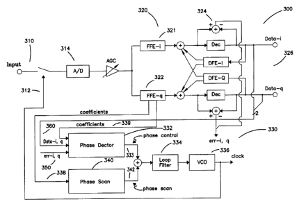
Fig. 3 illustrates a block diagram of the timing recovery system 300
according to the present invention. The timing recovery system 300 samples an
input
signal 310 according to a derived clock signal 312. The sampled input signal
310 is then
provided to an analog-to-digital converter 314. The digital output of the
analog-to-digital
converter 314 is passed through to a feed-forward equalizer 320 and a decision
feedback
equalizer 324 to produce the output data 326. The feed forward equalizer 320
adapts to
the line response so that the node immediately prior to the decision feedback
equalizer
(DFE) 324 sees no precursor intersymbol interference (ISI) which cannot be
cancelled.
3o The output of the feed-forward equalizer 320 also provides an input to a
phase-locked loop 330. The output of the feed-forward equalizer 320 is
provided to a
phase detector 332 for generating a phase control signal 333 that is provided
to a loop
filter 334. The loop filter 334 controls a voltage-controlled oscillator 336
to generate the
clock signal. However, in the timing recovery circuit 300 of Fig. 3,
coefficients 338 from
the feed-forward equalizer 320 are passed to a phase scanner 340 that provides
a phase
CA 02283180 1999-09-02
WO 98/39873 PCT/US98/04179
-6-
scan signal 342 which is combined with the phase control signal 333 from the
phase
detector 332.
The main phase detector 332 creates the useful timing information from
the several tap coefficient values 339 in the feed-forward equalizer 320,
error signals 350,
and recovered data 360. The frequency scan block 340 monitors the relation
between
feed-forward equalizer coefficient values 338 and when it judges that the
coefficient
values 338 are in the wrong state, the frequency scanner 340 forces the phase-
locked loop
330 to create a phase jump to eliminate the phase-locked loop from being stuck
at the
wrong stable phase.
to Two control signals 333, 342 from the main phase detector 332 and phase
scanner 340 respectively are added together and fed to the loop filter 334 to
drive the
voltage control oscillator. The controlled clock signal 312 then is used to
determine the
sampling instance of the input signal 310 which is quantized by the A/D
converter 314.
Figs. 4a and 4b illustrated the detail block diagrams for the main phase
detector 410 and the phase scan 450 respectively. In Fig. 4a, by way of
example, only
one feed-forward equalizer coefficient 412, H(nl), is used in the phase
detector. The
reference value 414, REF, is subtracted from coefficient H(nl) 412 which is
then
multiplied by the amplifier 416 by a gain factor 418, G. This process creates
one of the
two control signals, control-1 420.
2o On the other hand, the two products 422, 424 are calculated from the
combination of err-i 426, err-q 428, data-i 430, and data-q 432. The two
products 422,
424 are added 434 and integrated 436 by a factor, Z to generate the second
control signal,
control-2 440. The second control signal, control-2 440, is added with control-
1 to form
the final phase control signal 442 at the output of phase detector.
Fig. 4b illustrates an detailed embodiment for the phase scanner 450. In
Fig. 4b, two coefficients 452, 454 are compared in comparator 460. The output
462 of the
comparator 460 is a logic one if the first coefficient 452 to the comparator
460 is greater
than the second coefficient 454 to the comparator 460. The output 462 of the
comparator
460 is a logic zero if the first coefficient 452 to the comparator 460 is less
than or equal to
3o the second coefficient 454 to the comparator 460. The output 462 of the
comparator 460
is mixed with the scan phase 470 to generate the phase scan control signal
472.
Fig. 5 shows that CAP isolated pulses for I 510 and Q 520 pulses. These
pulses S 10, 520 are fed to the two parallel feed-forward equalizers, FFE-i
321 and FFE-q
322, respectively as shown in Fig. 3.
The waveforms 600 shown in Fig. 6 are the outputs of FFE-i 321 and FFE-
q 322 of Fig. 3 for those CAP isolated pulses. For example, for the case for
the null cable
CA 02283180 1999-09-02
WO 98/39873 PCT/US98/04179
-7_
and after feed-forward equalizers are converged, CAP I and Q isolated pulses
are fed to
the input at different times and plotted on the same time axis. As can be seen
in this
figure, plot A 620 and C 624 are the output of FFE-i 321 and FFE-q 322 when I
pulse is
sent and plot B 622 and D 626 are FFE-q 321 and FFE-i 322 outputs driven by
the CAP
Q pulse. Fig. 6 demonstrates that the timing information is created by the
combination of
products as shown below in equation 1.
Timing Information = err-q*out-i - err-i*out-q Eqn. 1
1 o Fig. 7 illustrates a detailed circuit diagram of a timing recovery circuit
700
according to the present invention. In Fig. 7, the center tap of the FFE-q 722
is used for
the H(nl) 770 previously described in Fig. 4a and Reference is set to zero.
The gain 772,
G, is set to 5Ø The comparison of +/-2 tap positions 774, 776 of FFE-q 721
is used to
drive the Phase Scanner 740 as described in Fig. 4b. The control of AGC is
performed
according to equation 2:
AGC=AGC-(err-i*out-i + err-q*out-q)/2**mue Eqn. 2
where AGC is the AGC gain and mue is the typically select to be in a range
between 14
2o and 20.
As shown in Fig. 7, the scan path 740 is used to eliminate the problem of
dual phase error compensations. The scan path forces the feed-forward
equalizer 720 not
to make a phase compensation. This can be done by monitoring the two feed-
forward
equalizer FFE-q 722 coefficient values: (H(n3)) 776 and (H(n2)) 774. This can
be
explained by looking at Fig. 5.
If the best timing phase is assumed to be the top of the I-signal, around
t=8.2 530, from the nature of the CAP signal, in this example, the Q-signal
has zero-
crossing 540 at around this optimal timing phase. When the feed-forward
equalizer tries
to compensate the phase error from this optimal timing, feed-forward equalizer
3o coefficients shown in Fig. 7, H(n2) 774 and H(n3) 776 will change their
values. For
example, when the phase is delayed, the H(n2) 774 value becomes bigger and
H(n3) 776
becomes smaller. The scan control 740 uses these characteristics and when it
detects that
the feed-forward equalizer FFE-q 722 has over-compensated for the phase error,
the scan
control 740 sends an output 742 which is added to phase control signals
control-1 780 and
control-2 782. Thus, the scan control eliminates dual phase error
compensation.
CA 02283180 1999-09-02
WO 98/39873 PCT/US98/04179
_g_
The foregoing description of the exemplary embodiment of the invention
has been presented for the purposes of illustration and description. It is not
intended to be
exhaustive or to limit the invention to the precise form disclosed. Many
modifications
and variations are possible in light of the above teaching. It is intended
that the scope of
the invention be limited not with this detailed description, but rather by the
claims
appended hereto.