Note: Descriptions are shown in the official language in which they were submitted.
CA 02283359 1999-09-24
POWER TRANSFORMER WITH INTERNAL DIFFERENTIAL MODE
DISTORTION CANCELLATION
Field of the Invention
This invention relates in general to power transformers and more particularly
to a power transformer design with internal circuitry for canceling
differential mode
harmonic distortion.
Background of the Invention
Power transformers are well known in the art for providing rated voltage and
1 o current to electric and electronic devices while isolating those devices
from the AC
current mains. Ideally, the mains should deliver pure undistorted sinusoidal
signals to
the primary side of the power transformer. However, in practical applications,
this is
often not the case. Harmonic components of the fundamental frequency (50 or 60
Hertz) are almost always present, as well as unrelated higher frequency
voltages
~5 which may be caused by any of a number of sources. For example, spike
signals from
lightning or the switching of motors, radio frequency signals, digital signals
from
computer systems, asymmetrical loading of the mains, communication signals,
etc.,
all may contribute to harmonic distortion of the mains power signal.
It is also known that such distortion can, depending on severity, interfere
with
2o the optimal functioning of the electrical or electronic equipment connected
to the
mains, or cause damage to the equipment. In Europe, for instance, three
classes have
been defined under the recent CE regulations relating to mains distortion.
Class A
equipment is insensitive to distortion. Class B equipment is influenced to a
limited
extent by mains distortion without affecting fundamental tasks. Class C
equipment
25 ceases functioning under the influence of distortion, but by resetting the
equipment,
the functioning of the equipment can continue.
Accordingly, the elimination of mains distortion is widely recognized in the
art as being highly desirable.
One solution to the problem of eliminating harmonic distortion involves
3o rectifying and buffering the distorted signal to create new pure
undistorted sinusoidal
voltage signals. This solution is well known in the art of uninterruptable
power
supplies for use with computers.
CA 02283359 1999-09-24
Another prior art solution involves the use of resonant transformers which
resonate only at the fundamental frequency and therefore attenuate all other
frequencies.
Yet another solution involves the creation of "balanced" power lines by means
of an external isolation transformer wherein the center tap of the secondary
winding is
connected to ground, thereby creating two outputs which pass the differential
mode
distortion in opposite phase.
In all of the foregoing prior art solutions, external elements are required to
be
added to the power transformer in order to remove differential mode
distortion. These
to solutions introduce additional circuit complexity and attendant costs.
A sample of exemplary prior art patents in the field of transformer means
distortion cancellation include:
US Patent 5,640,314 (Glasband et al)
US Patent 5,343,080 (Kammeter)
~ 5 US Patent 5,206,539 (Kammeter)
US Patent 5,434,455 (Kammeter)
Summary of the Invention
According to the present invention, a power transformer is provided with a
series connected auxiliary coil and high-pass filter connected in opposite
phase to the
20 main coil in one or both of the main and secondary windings, so that high
frequency
harmonic distortion is magnetically canceled in the core of the transformer
while the
fundamental power frequency passes unattenuated. This structure provides a
unique
advantage over prior art designs by eliminating costly and expensive external
filtering
circuitry. Furthermore, according to an aspect of the invention the
transformer
25 characteristics (transfer function, impedance, current and phase angle) may
be
controlled by varying circuit parameters of the transformer.
Brief Description of the Drawings
A detailed description of the preferred embodiment and alternative
embodiments is provided herein below with reference to the following drawings,
in
3o which:
Figure 1 is a schematic illustration of the power transformer according to the
present invention with series auxiliary coil and high pass filter connected in
opposite
phase to the primary coil;
Figure 2 is a graph showing power transfer across the transformer of Figure 1
35 as a function of frequency;
CA 02283359 1999-09-24
Figure 3 is a power transformer according to a first alternative embodiment of
the present invention with auxiliary coil and high-pass filter connected in
opposite
phase to the secondary transformer coil;
Figure 4 is a schematic illustration of a power transformer according to a
further alternative embodiment of the present invention with auxiliary coils
and high
pass filter elements connected in opposite phase to both the primary and
secondary
transformer coils;
Figure 5 is a schematic illustration of an embodiment of the invention similar
to Figure 1 wherein the high pass filter element is implemented using a single
to capacitor;
Figure 6 is a detailed circuit diagram of a preferred embodiment of the
invention;
Figure 7 is a schematic illustration similar to Figure 1 with a resistance
connected in series with the capacitance, thereby forming the high-pass filter
device,
15 and with references added representing the number of turns, inductance,
internal
magnetic wire resistance, impedance and mutual inductance of the transformer;
Figures 8A-8D show the transfer function, total primary impedance, total
primary current from the mains, and phase angle between primary voltage and
current
as a function of frequency for the circuit of Figure 7 wherein the primary and
auxiliary
20 winding are bifilar constructed;
Figures 9A-9D represent the same relationships as Figures 8A-8D for the
circuit of Figure 7 wherein the primary windings are bifilar but with an
increased
internal plus external resistance in the auxiliary winding;
Figures l0A-l OD represent the same relationships as Figures 9A-9D for the
25 circuit of Figure 7 wherein the additional series capacitance is raised to
a higher
capacitance level; and
Figures 11A-11D represent the same relationships as Figure 8A-8D for the
circuit of Figure 7 where the windings are not bifilar constructed.
Detailed Description of the Preferred and Alternative Embodiments
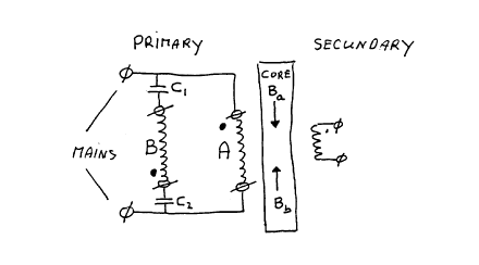
Turning to Figure 1, a power transformer is shown according to the present
invention comprising a primary side and secondary side separated by a magnetic
core,
CA 02283359 1999-09-24
4
in the usual manner. However, in accordance with the present invention, an
auxiliary
primary coil B is provided having the same number of turns as the main primary
winding A, but connected in opposite phase thereto. Furthermore, a pair of
capacitors
C, and C2 are connected in series with the auxiliary coil B, forming a high
pass filter.
It will be apparent to persons of ordinary skill in the art that the high pass
filter
function may be implemented using a single capacitor, series capacitor and
resistor,
or any other appropriate frequency dependent structure, and is not limited to
the two-
capacitor implementation shown in Figure 1.
According to the preferred embodiment, the windings A and B are of bifilar
to construction. However, as discussed in greater detail below, this is not a
requirement
of the invention. Indeed, as discussed in greater detail below, optimal tuning
of the
mutual coupling between the windings permits control of the transformer
transfer
function, phase angle between primary currents and voltages and total primary
impedance. In fact, the main and auxiliary windings may be characterized by
any
15 reasonable mutual coupling between zero (i.e. none) and almost one (i.e.
bifilar).
The selection of bifilar windings A and B ensures very small leakage between
the two windings, so that each winding exercises the same magnetic effect on
the core
of the transformer.
The values of the capacitors C, and Cz are chosen such that above the mains
2o fundamental frequency, the primary impedance becomes small. At such
frequencies,
the capacitors C, and CZ behave as short circuit elements. Accordingly, high
frequency distortion in the mains power signal result in currents flowing in
opposite
directions through both windings A and B. These currents result in magnetic
flux
densities Ba and Bb in the transformer coil. Since the magnetic flux densities
Ba and
25 Bb have equal magnitude but opposite phase, they cancel out, resulting in
zero flux
density in the core of the transformer at frequencies above the cut off
frequency of the
high-pass filter device.
Figure 2 is a simplified graph showing the transfer of power, in dB, from the
primary side to the secondary side of the transformer of Figure 1 as a
function of
3o frequency. According to the prior art, (i.e. transformer design without
distortion
elimination), the pass band for high frequency distortion signals is large. By
way of
contrast, according to the present invention, distortion signals above the
high-pass
filter cut off frequency are significantly attenuated.
CA 02283359 1999-09-24
Figure 3 shows an embodiment of the invention in which the auxiliary coil B
is connected in opposite phase to the main coil A on the secondary side of the
transformer. Thus, where the load generates high frequency distortion signals
(e.g. as
a result of digital switching), these signals are coupled to the transformer
core with
equal and opposite phase by the secondary coils A and B, whereas the mains
fundamental frequency signals are passed only by the secondary coil A, having
been
filtered by capacitors C, and Cz connected to coil B. This configuration is
useful for
preventing high frequency signals generated on the secondary side from being
passed
to the power mains.
to Figure 4 shows an embodiment of the invention with distortion canceling
auxiliary coils B and B' and high pass filter devices C,, C2, and C , , C 2
connected to
the main coils in both the primary and secondary sides of the transformer.
Figure 5 shows an embodiment of the invention similar to Figure l, wherein
only a single capacitor C is used to implement the high pass filter function.
is Thus, according to a general aspect of the present invention, a power
transformer is provided wherein the net flux density in the magnetic core is
canceled
for frequencies above the cut off frequency of a high-pass filter in the
auxiliary coil
(Figures l, 3 and 5) or multiple auxiliary coils (Figure 4). A further feature
of the
invention is that high frequency flux density outside the transformer is
canceled as
2o well, thereby creating smaller external leakage field strength which
permits higher
packaging densities in electronic circuit design.
The present invention is useful in canceling differential mode distortion. The
transfer of common mode distortion through the transformer also takes place as
a
result of capacitance coupling between the primary and secondary windings. In
order
25 to stop this transfer, the capacitive coupling between the windings must be
minimized.
This can be realized by adding electromagnetic shields between the primary and
secondary windings, or by implementing special winding configurations in a
well
known manner. The canceling of common mode distortion does not form part of
the
present invention.
3o Turning now to the detailed circuit of Figure 6, a power transformer is
shown
according to the preferred embodiment a power cord of an electronic device S
is
connected to phases 1 and 2 of a mains power supply. Phase 3 of the power
supply is
connected to ground and the chassis of the device, in a well known manner. In
some
CA 02283359 1999-09-24
cases, grounding of the electronic equipment may not be required. Within the
chassis
of the equipment or device 5 an on/off switch 6 is provided as well surge
protector 8,
for connecting and disconnecting the power mains from the equipment.
The power transformer according to the present invention is designated by
reference numeral 7. The power mains are connected to primary winding 9 of the
power transformer. The phase of the coil is indicated by a dot 18 (wherein
phase
denotes the direction of the winding (i.e. right handed or left handed
winding)). The
mains voltage causes an alternating current 10 to flow through the primary
winding 9.
The current 10 creates an alternating flux density 13 in the magnetic core 11
of the
1 o transformer 7.
A second or auxiliary primary winding 14 is provided at the primary side of
the transformer, which may either by bifilar round with the primary winding 9
or, as
discussed in greater detail below, may be wound in a non-bifilar construction.
For the
bifilar construction, windings 9 and 14 have the same number of turns and
exhibit
15 identical mutual conductance with secondary core 20 via the magnetic core
11.
As shown, the winding 14 is connected in parallel with winding 9 but with
opposite phase (dot 19). A passive filter element 15 (e.g. capacitor) is
connected in
series with the winding 14. As discussed above, the implementation of the
present
invention is not restricted to a single capacitor. Two capacitors may be used
(one on
2o either side of the winding 14, as shown in Figure 1 ) or any other
frequency dependent
structure which functions as a high-pass filter. In general, the high-pass
filter element
will be of passive construction with an impedance which is inverse to the
frequency of
signals applied thereto. Other topologies including combinations of inductors
and
capacitors and resistors may also be used, as well as active filter
structures.
25 An alternating current 16 flows through winding 14 creating an alternating
magnetic flux density 17 in the core of the transformer. Because the primary
windings 9 and 14 are connected with opposite phase, the flux density 17 in
the core
11 is characterized by an opposite vectorial direction to the flux density 13
created by
winding 9. The flux densities 13 and 17 therefore cancel out within the
magnetic
3o core, wherein the degree of cancellation depends on the frequency of the
signal from
the mains, the number of turns of windings 9 and 14 and the frequency
dependencies
of the filter 15, as discussed in greater detail below with reference to
Figures 7-11.
CA 02283359 1999-09-24
For very high frequency signals, the impedance of the filter element 1 S can
be
considered to be zero. Where the number of turns in the primary windings 9 and
14
are equal, the flux densities 13 and 17 are equal in magnitude and opposite in
phase at
the given frequency, thereby canceling each other out completely. The net flux
density in the core therefore equals zero at high frequency. Accordingly,
there is no
coupling of the high frequency signals across the magnetic core to the
secondary
winding 20.
From the foregoing, it will be apparent that the impedance behavior of the
element 15 determines at what frequency the differential mode distortion
signals are
o canceled. Thus, the value of the filter element 15 can be chosen such that
at the mains
fundamental frequency its impedance is sufficiently large that the current 16
in
winding 14 becomes negligible. Then, only the flux density 13 of winding 9 is
present in the core 11 and creates an unrestricted voltage in the secondary
winding 20.
At higher frequencies, the impedance of the filter element 15 decreases,
thereby
15 creating the scenario discussed above wherein the net flux density in the
core 11
vanishes to almost zero. By selecting predetermined impedances of the filter
element
15, the total transfer bandwidth of the transformer can be tuned to exhibit
different
behavior for different applications, as discussed below.
In the foregoing embodiments, the high pass filter device (e.g. device 15 in
2o Figure 6) is characterized by a first order high-pass filter structure.
Where second or
higher order high pass filter structures are required, the device 15 can be
replaced by
combination of external inductors and capacitors. Thus, it is possible to
create a filter
structure with the use of active amplifying elements combined with resistors,
capacitors and inductors for sensing high frequency content on both the
primary and
25 secondary windings and actively regulating the net high frequency content
in the core
to zero. Enhancements of this sort are contemplated by the inventor as being
within
the scope of the present invention.
Turning now to Figure 7, an embodiment of the invention is shown which is
similar to Figure 1, but which specifies and identifies parameters of the
transformer
3o for the purpose of elucidation. Thus, the main primary winding Pl is
characterized by
having Np turns, an inductance LP and internal magnetic resistance R;p, and is
connected to the mains having mains frequency f(x). On the secondary side of
the
transformer, a secondary winding S is provided with NS turns, an inductance LS
and
CA 02283359 1999-09-24
secondary load ZS connected thereto (the internal resistance of the winding S
is
included in ZS). The auxiliary winding P2 plus filtering capacitor C is
provided
according to the invention with Np turns, an inductance Lp, and an internal
plus
external resistance R;p2. The relative phase of the winding P2 with respect to
winding
P1 is indicated by the black dot, in the usual manner.
The winding P1 exhibits a mutual inductance toward winding P2 of MP kp ~ Lp
in which lcp is the coupling coefficient between the primary windings P1 and
P2.
Winding P 1 exhibits a mutual inductance with respect to winding P3 of MSc =
ks
LP LS . Winding P2 exhibits a mutual inductance towards the secondary windings
to P3 of MSZ=k2 ~ MS,, which indicates that the mutual coupling from between
windings
P2 and P3 does not have to equal to the mutual coupling from windings P l and
P3.
Turning to Figures 8-11, different tuning scenarios are set forth resulting
from
the selection of different operating parameters for the transformer. In each
of Figures
8-11 the first graph (graph A) illustrates the transfer function H(x) from
input to
15 output in dB for a frequency range f(x)=l OHz to 100 kHz. According to this
graph, a
normalized transfer function is considered (i.e. NS/NP 1). The second graph
(graph B)
shows total primary impedance ZP(x) of the transformer plus secondary load as
measured between the input terminals (i.e. as connected to the mains). The
vertical
axis in this graph is in k52. In the third graph (graph C), the total primary
current
2o delivered from the mains to the transformer is shown (IP(x)=Vmains/ZP(x)).
The
final graph in each of Figures 8-11 (graph D) shows the phase angle OZp(x)
between
the primary voltage and current (in degrees).
Turning to the scenario of Figure 8, the parameters of the circuit in Figure 7
were chosen such that the windings P1 and P2 were ofbifilar construction (i.e.
k2=1).
2s The mains voltage was 230 VAC and primary inductance Lp = 200 H. The
primary
winding wires were of equal diameter (i.e. R;P,=R;PZ 0.352). The capacitor C
was
selected to be 8.8 x 10⁻⁹F such that at 60 Hertz (the fundamental means
frequency) the
phase angle became zero degrees.
As shown in Figure 8A, an undamped series resonance developed at SkHz
3o where the primary impedance was minimal (i.e. exhibiting reflective
behavior) and the
primary current therefor was maximized at S kHz. Accordingly, with this
selection of
parameters, bifilar tuning resulted in large high frequency currents.
CA 02283359 1999-09-24
9
For the scenario of Figure 9, the parameters of circuit 7 were similar to
those
of the scenario of Figure 8 except that the internal plus external resistance
R;p2 of the
secondary primary winding P2 was increased to l OkS2 so as to damp the
resonance
which had been found at S kHz.
Accordingly, with reference to Figure 9A, the slope of the transfer function
is
seen to have changed. Specifically, the increase in primary current at 5 kHz
has been
reduced. From Figure 9D it will be seen that the phase angle at 60 Hz remains
unaffected. Accordingly, by changing R;PZ, the slope of the transfer function
and the
reflecting behavior of the total transformer can be modified.
to Turning to Figure 10, a similar circuit configuration for Figure 7 was
adopted
as in the scenario for Figure 9 except that the capacitance of capacitor C was
increased
to 8.8 x 10-gF (ten times relative to the scenarios for Figures 8 and 9). As
seen from
Figure l OD, the phase angle between the primary current and primary voltage
is no
longer zero degrees at 60 Hz, but has become zero degrees at 20 Hz. From this,
it can
1s be concluded that by varying the capacitance C, the phase angle between
primary
current and primary voltage can be influenced.
Turning finally to the scenario of Figure 11, the parameters were selected to
be
the same as for the configuration of Figures 8 and 9 except that the windings
P 1 and
P2 were not bifilar constructed. Instead, winding P 1 was wound around the
entire
2o toroidal magnetic coil, whereas winding P2 was segmented (e.g. in the area
between
12 and 3 o'clock in radial degrees around the core) resulting in an increase
in R;pz to
100kS2 Consequently, the primary mutual coupling MP becomes less, and the
mutual
couplings MS, and MSZ become unequal (in the present case k2=0.9). The
capacitor C
was chosen to have the same value as in the cases set forth with reference to
Figures 8
25 and 9, resulting in a zero degree phase at 60 Hz between primary current
and voltage.
The resistance R;PZ was increased to 100kS2 to remove the series resonance at
5 kHz.
Accordingly, it will be appreciated from Figures l0A-lOD that the cut off
frequency and the slope of the effective low pass filter function of the power
transformer can be influenced by changing the mutual coupling between the
different
3o windings. Impedance increases as a function frequency resulting in very
small high
frequency primary currents (i.e. non-reflecting behavior), while the primary
current at
60 Hz is seen to be influenced mainly by the secondary load ZS.
CA 02283359 1999-09-24
From the different case studies presented for the circuit of Figure 7 having
regard to the parameters chosen with reference to Figures 8-11, it will be
seen that the
use of different parameters for the transformer of the present invention
allows for
influencing the transfer function of the transformer, such as cut-off low pass
frequency, effective slope of the transfer function, tuning of the phase angle
between
primary currents and voltages as well as the phase angle between secondary
voltages
and currents, etc.
Additional modifications and variations of the invention may be conceived by
persons of ordinary skill in the art. All such modifications and variations
are believed
1o to be within the sphere and scope of the invention as defined by the claims
appended
hereto.