Note: Descriptions are shown in the official language in which they were submitted.
_ CA 02283897 1999-09-16
Substitute Sheet
Attorney Docket No. 8194-74
BUS ARBITRATORS FOR COMMON LOCAL OSCILLATORS
IN CELLULAR RADIOTELEPHONE BASE STATIONS
Field of the Invention
The present invention <~enerally relates to cellular communications
systems. and more particularly. to the inte~~ration of two transceivers onto a
sin~~le
circuit board in a cellular radiotelephone base station.
Background of the Invention
Cellular communications systems are commonly employed to
provide voice and data communications to a plurality of mobile units or
subscribers. Analog cellular systems, such as those designated AMPS. ETACS.
NNIT-4~0, and NIVIT-900, have been deployed successfully throughout the world.
More recently, digital cellular systems such as those designated IS-~4B in
North
America and the Pan-European GSM system have been introduced and deployed.
These systems and other systems are described, for example, in the book
entitled
Cellular Radio Systems by Balston, et al., published by Artech House, Norwood,
NIE, 1993 and European Patent Application Publication EP 0 696 112 A2.
Frequency reuse is commonly employed in cellular technology
wherein groups of frequencies are allocated for use in regions of limited
geographic coverage known as cells. Cells containing equivalent groups of
frequencies are geographically separated to allow mobile units in different
cells to
simultaneously use the same frequency without interfering with each other. By
doing so, many thousands of subscribers may be
-1-
r
CA 02283897 1999-09-16
WO 98/45958 PCT/US98/06534
served by a system with only several hundred frequencies. In the United
States, for example, Federal authorities have allocated to cellular
communications a block of the UHF frequency spectrum that is further
subdivided into pairs of narrow frequency bands called channels. Channel
pairing results from the frequency duplex arrangement wherein the transmit
and receive frequencies in each pair are offset by 45 megahertz (MHz). At
present, there are 832, 30-KHz wide, radio channels allocated to cellular
mobile communications in the United States. To address the capacity
limitations of this analog system, a digital transmission standard designated
IS-54B has been provided, wherein those frequency channels are further
subdivided into three time slots.
In addition, capacity limitations have been addressed by using
microcells, that is, low power cellular transmissions that provide coverage
over a smaller area. The smaller microcells allow more cells to exist within
a predefined geographic area, thereby increasing the number of users that
can be serviced within that geographic area. A particular application of
microcell technology is indoor cellular radiotelephone services.
As illustrated in FIG. 1, an indoor cellular communication
system 20 as in the prior art includes one or more mobile stations or units
22, one or more wall mounted base stations 24, a radio control interface
26, and a mobile switching center (MSC) 28. Although only one cell 30 is
shown in FIG. 1, a typical indoor cellular network may have several cells
30, each cell usually being serviced by one or more wall mounted base
stations 24. The number of wall mounted base stations 24 depends on the
channel capacity of the cell 30. Each wall mounted base station typically
supports anywhere from 4-12 channels, depending upon its site. The cell
typically has one or more control channels and one or more voiceldata
(hereafter referred to as "traffic") channels allocated to it. The control
channel typically is a dedicated channel used for transmitting cell
30 identification and paging information.
Each wall mounted base station 24 is connected to the radio
control interface 26 by a radio interface link 32. The radio control interface
-2-
E~, .; ~i-~,~~,. c~
~~~Y
CA 02283897 1999-09-16
WO 98/45958 PCT/US98/OG534
26 exchanges signals between the wall mounted base stations 24 and the
mobile switching center 28. Specifically, the radio control interface 26
converts the traffic and control information from the format received over
the radio interface links 32 into a format suitable for transmission over a
dedicated transmission link 34 interconnecting the radio control interface
(RCI) 26 to the MSC 28. In the reverse direction, the RCI 26 converts the
traffic and control information received over transmission link 34 into a
format suitable for transmission over radio interface links 32 to the
respective base stations 24.
The MSC 28 is the central coordinating element of the overall
cellular network 20. It typically includes a cellular processor 36 and a
cellular switch 38, and provides an interface to the public switched
telephone network (PSTN) 40. Through the cellular network 20, a duplex
radio communication link 42 may be effected between two mobile units 22
and a landline telephone user 44. The function of the base stations 24 is
commonly to handle the radio communications with the mobile units 22.
In this capacity, the base stations 24 also supervise the quality of the link
42
and monitor the received signal strength from the mobile units 22.
A typical wall mounted base station 24 as in the prior art is
schematically illustrated in FIG. 2. The base station 24 includes a radio link
interface 50, a power supply 52, and one or more communication channel
transceiver boards 54. In addition, the base station includes an antenna 56
associated with each of the communication channel transceiver boards 54.
The radio link interface 50 provides an interface between the radio control
interface 26 and the communication channel transceiver boards 54. In
essence, the radio link interface 50 multipiexes/demultiplexes the signals
to/from the radio control interface 26 for use by the communication channel
transceiver boards 54. The power supply 52 provides power to the other
components of the base station 24.
Further, the base station 24 includes a number N of
communication channel transceiver boards 54 for effectuating radio
communications with mobile units 22. Power for each of the
-3-
CA 02283897 1999-09-16
WO 98/45958 PCT/ITS98/06534
communication channel transceiver boards is supplied by the power supply
52. Traffic and control signals are exchanged between the communication
channel transceiver boards 54 and the radio link interface 50 over
respective lines 58. In addition, the communication channel transceiver
boards 54 are interconnected with one another by links 60 so that the
transceiver boards 54 can receive traffic signals from more than one antenna
56 for reception diversity.
Each communication channel transceiver board 54 typically
comprises a circuit board 66 having a single transceiver 68, for example, a
radiotelephone, as illustrated in FIG. 3. The transceiver 68 includes a
controller 70, a receive local oscillator (RXLO) 72, a transmit local
oscillator
(TXLO) 74, a frequency generator (FG) 76, a duplexer 78, an antenna 79,
mixers 80 in the receive signal path, and mixers 81 in the transmit signal
path. The controller 70 communicates with the RXLO 72, TXLO 74, and
FG 76 to control the conversion of received radio frequency (RF) signals
down to a baseband frequency for processing, and for the conversion of
transmit signals to a radio frequency (RF) signal for transmission over the
communication link 42. Further, the controller 70 exchanges traffic and
control signals with the mobile switching center 28 via the radio link
interface 50 and the radio control interface 26.
The RXLO 72, TXLO 74 and FG 76 are each configured to
receive tuning information such as a division ratio from the controller 70 for
generating a stable frequency signal used in performing conversion of the
traffic signal in the receive signal path via mixer 80 and in the transmit
signal path via mixer 81.
For example, in the receive signal path, the RF signal may be
converted down to a receive intermediate frequency by subtracting the FG
76 signal from the RF signal at the mixer 80 associated with the FG 76. In
general, the two signals are added by the mixer 80 and filtering is used to
isolate the resulting term that represents the difference of the two signals.
The division ratio or tuning information is sent by the controller 70 to the
FG 76 at power up or activation of the transceiver 68. This first conversion
-4-
CA 02283897 1999-09-16
WO 98/45958 PCT/US98/06534
of the received signal is referred to as the first down conversion stage in
the
received signal path. Next, the RXLO 72 further converts the received
signal from the receive intermediate frequency to a base band frequency by
further mixing the signal with a second frequency signal generated by the
RXLO 72 at the mixer 80 associated with the RXLO 72. Filtering is then
used to isolate the term that represents the difference of the two signals.
The division ratio for the second frequency signal is also sent by the
controller 70 to the RXLO 72 at power up. This is referred to as the second
down conversion stage in the received signal path. At the base band
frequency, the received traffic signal can then be processed by the digital
control logic of the transceiver 68. In a like manner, traffic signals in the
transmit signal path are initially converted from a baseband frequency to a
transmit intermediate frequency in the first up conversion stage at the mixer
81 associated with the TXLO 74 using a division ratio provided to the TXLO
74 by the controller 70. The traffic signal is then converted up from the
transmit intermediate frequency to a radio frequency in the second up
conversion stage at the mixer 81 associated with a FG 76.
Note that the transmit intermediate frequency generally is
mixed with the same local oscillator frequency used in the first down
conversion in the received signal path. Therefore, if the same local
oscillator frequency is used in both the first down conversion stage in the
received signal path and the second up conversion stage in the transmit
signal path, then only one FG 76 would be needed for transceiver 68.
However, since the transmit and receive intermediate frequencies differ, a
separate local oscillator may be necessary for each of the receive signal path
and the transmit signal path so that the frequencies may be converted
to/from the baseband frequency.
The RXLO 72, TXLO 74, and FG 76 can be programmed with
respective division ratios in the following manner. During each power up
or activation of the transceiver 68, the controller 70 sends several
commands over a serial bus 84 which interconnects the controller 70 with
the RXLO 72, the TXLO 74, and the FG 76. Each command sent over the
-5-
CA 02283897 1999-09-16
WO 98/45958 PCT/US98/06534
serial bus 84 is addressed to a separate one of the RXLO 72, TXLO 74 and
FG 76. The commands typically comprise a clock signal sent over one line
of the bus, a M-bit data word sent over another line of the bus, and a select
signal sent over one of the remaining lines of the serial bus, wherein each
of the remaining bus lines is dedicated to one of the RXLO 72, TXLO 74 or
FG 76. Each of the RXLO 72, TXLO 74 and FG 76 has a register that
receives the data word sent over the serial bus, though the data is only read
into the device if a select signal designating that device is also received.
Otherwise, the data word is merely shifted out of the register and the data
word associated with the next select signal is shifted in with the next
command. Thus, when the controller 70 writes to the RXLO 72, all three
devices receive the data word but only the RXLO 72 actually reads because
it is the only device that receives a select signal that identifies the RXLO
72.
Indoor cellular systems such as the one described above have
become widely popular for several reasons. First, a cellular customer cari
use the same telephone everywhere he/she goes. Second, the cellular
telephone of the customer does not need additional circuitry to allow for
indoor use as do some cellular telephones that operate as cordless
telephones indoors. Third, indoor cellular systems provide larger coverage
areas indoors than do typical cellular telephones operating in a cordless
mode indoors. Fourth, the capacity of an indoor cell can be increased
easily by adding additional wall mounted base stations.
However, a limitation of indoor cellular systems is the size
and cost of the wall mounted base stations 24. The size of a wall mounted
base station 24 can easily become obtrusive when designed to include more
circuit boards 66 so as to increase channel capacity. Thus, endlessly adding
more circuit boards to increase the number of channels is usually not a
viable option. Therefore, additional wall mounted base stations must be
added at a sizeable cost. Therefore, a need exists in the market for smaller
and less obtrusive wall mounted base stations that cost less and service
more channels.
-6-
CA 02283897 1999-09-16
WO 98/45958 PCT/US98/06534
Summary of the Invention
It is therefore an object of the present invention to provide a
cellular base station with a transceiver circuit board having two separate
S transceivers that share common resources.
It is another object of the present invention to provide a
cellular base station transceiver circuit board having two transceivers that
share a common local oscillator.
It is another object of the present invention to provide two
cellular base station transceivers that share a common local oscillator
without any handshaking or communication between the two transceivers.
It is yet another object of the present invention to provide a
cellular base station having a reduced size, fewer parts, and lower cost than
prior art base stations configured for indoor use.
These and other objects of the present invention are provided
by a cellular radiotelephone base station that is configured for indoor use
and that includes a transceiver circuit board having two transceivers and an
arbitrator for managing shared resources such as common local oscillators
thereon. During power up or activation of the transceivers, the arbitrator
detects the first one of the transceivers that tries to send a command to the
common local oscillator and then connects the controller of that transceiver
to the shared common local oscillator to the exclusion of the other
transceiver. Since the controllers send the same command to the common
local oscillator at power up, it does not matter which one actually
communicates the command to the common local oscillator. Therefore, the
control logic of the controllers does not need to be modified for the present
invention, nor do the controllers need to communicate with one another
when writing a command to the shared common local oscillator. Further,
because the transceivers share the common local oscillator, fewer parts may
be used on the transceiver circuit board, which can reduce both the cost
and size of the transceiver circuit boards, and thus, the cost and size of the
wall mounted base stations.
_7_
CA 02283897 1999-09-16
WO 98/45958 PCT/US98/06534
In particular, according to the present invention, a circuit
board for use in a cellular radiotelephone base station comprises a first
cellular radio transceiver including a first controller that controls the
operation of the first transceiver, a second cellular radio transceiver
including a second controller that controls the operation of the second
transceiver, a common local oscillator that generates a frequency signal for
use by the first and second transceivers in tuning a radio signal, and an .
arbitrator that is connected to the first and second controllers and that
determines which of the first and second controllers communicates with the
common local oscillator.
In accordance with a feature of the present invention, the
arbitrator may be connected to the first and second controllers by first and
second bus lines, respectively, wherein the arbitrator monitors the first and
second bus lines to determine the first one of the controllers that attempts
to
communicate with the common loca) oscillator so that the controller which
attempts to communicate with the common local oscillator first is given
control of the common local oscillator to the exclusion of the other
controller. In addition, the arbitrator is responsive to a reset signal from
the
controller that has control for resetting the arbitrator so that the
controllers
may once again vie for control of the common local oscillator.
In accordance with another feature of the present invention,
the circuit board may include a second common local oscillator that is
shared by the first and second transceivers in substantially the same manner
as described above. For instance, the first common local oscillator may be
provided for tuning radio signals in the received signal paths of the first
and
second transceivers, and the second common local oscillator may be
provided for tuning radio signals in the transmit signal paths of the first
and
second transceivers. Therefore, only two local oscillators are necessary for a
circuit board having two transceivers.
The arbitrator can be implemented as a state machine by a
programmable device such as a programmable logic device (PLD), a
programmable array logic (PAL) device, a field programmable gate array
_g_
CA 02283897 1999-09-16
WO 98/45958 PCT/US98/06534
(FPGA) device, a complex programmable logic device (CPLD) or an
application specific integrated circuit (ASIC). Alternatively, the arbitrator
can be implemented by a programmable device in combination with a
tristate buffer. In the case of the latter, the programmable device monitors
the first and second serial buses and sends a connect signal to the tristate
buffer that either connects the first serial bus or the second serial bus to
the
common local oscillator when one of the controllers first attempts to
communicate with the common local oscillator. As before, the
programmable device can be any suitable programmable device such as a
PLD, PAL, FPGA, CPLD or ASIC device.
A method in accordance with the present invention for sharing
a common local oscillator by a first transceiver and a second transceiver that
are co-located on a circuit board and configured for use in a cellular
radiotelephone base station, wherein the first transceiver includes a first
controller and the second transceiver includes a second controller,
comprises the following steps. One step includes detecting when one of
the first and second controllers attempts to communicate with the common
local oscillator. Another step includes connecting the controller that
attempts to communicate with the common local oscillator to the common
local oscillator for line communication therebetween. A further step
includes monitoring the first and second controllers for a signal to determine
which of the first and second controllers attempts to communicate with the
common local oscillator first.
Other features and advantages of the present invention will
become apparent to one with skill in the art upon examination of the
following drawings and detailed description. It is intended that all such
additional features and advantages be included herein in the scope of the
present invention, as defined by the appended claims.
_g_
CA 02283897 1999-09-16
WO 98/45958 PCT/US98/06534
Brief Descri~~tion of the Drawings
FIG. 1 is a schematic block diagram illustrating basic
components of an indoor cellular communication system as in the prior art;
FIG. 2 is a schematic block diagram illustrating the functional
components of a wall mounted base station of the indoor cellular
communication system of FIG. 1;
FIG. 3 is a schematic block diagram iilustrating the functional
elements of a communication channel transceiver board of the wall
mounted base station of FIG. 2;
FIG. 4 is a schematic block diagram illustrating the functional
elements of a communication channel transceiver board of a wall mounted
base station according to the present invention;
FIG. 5 is a schematic block diagram illustrating the functional
elements of a communication channel transceiver board in accordance with
the present invention, wherein the arbitrator is implemented by a
programmable array logic device and a tristate buffer; and
FIG. 6 is a state diagram illustrating the operation of an
arbitrator according to the present invention.
Description of Preferred Embodiments
The present invention will now be described more fully
hereinafter with reference to the accompanying drawings, in which
preferred embodiments of the invention are shown. This invention may,
however, be embodied in different forms and should not be construed as
limited to the embodiments set forth herein. Rather, these embodiments are
provided so that this disclosure will be thorough and complete, and will
fully convey the scope of the invention to those skilled in the art. The
elements of the drawings are not necessarily to scale, emphasis instead
being placed upon clearly illustrating the principles of the present
invention.
Furthermore, like reference numbers refer to like elements throughout.
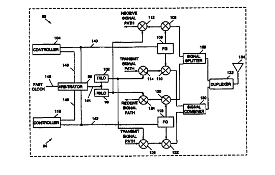
With reference to FIG. 4, illustrated is a dual transceiver board
90 in accordance with the present invention. The dual transceiver board 90
-10-
CA 02283897 1999-09-16
WO 98/45958 PCT/US98/06534
is suitable for implementation, or instance, in the wall mounted base station
24 (FIG. 2) of the indoor cellular communication system 20 (FIG. 1 ). The
dual transceiver board 90 includes a first transceiver 92 and a second
transceiver 94 integrated thereon. This is a particularly advantageous
configuration for an indoor wall mounted base station because the size of
the base station is critical for indoor cellular systems where the base
stations
are mounted to a wall in a work area of a building. A wall mounted base
station incorporating dual transceiver boards only needs half the number of
transceiver boards as previously needed to provide the same number of
channels. Thus, the size of the wall mounted base station can be reduced
from that of conventional wall mounted base stations.
The dual transceiver board 90 also includes an arbitrator 96
for managing common resources shared by the first and second transceivers
92, 94. For purposes of the present disclosure, the shared resources are a
receive local oscillator (RXLO) 98 and a transmit local oscillator (TXLO)
102. Thus, rather than providing a separate RXLO and TXLO for each of
the first and second transceiver 92, 94, the present invention provides for
the sharing of a single RXLO 98 and a single TXLO 102 by both transceivers
92, 94, thereby reducing board space, part count, and costs associated with
a wall mounted base station.
The first transceiver 92 includes a controller 104, RXLO 98,
TXLO 102, a frequency generator (FG) 106, and mixers 108, 110, 112, and
114. Likewise, the second transceiver 94 includes a controller 116, RXLO
98, TXLO 102, a FG 118, and mixers 120, 122, 124, and 126. The first
and second transceivers 92, 94 are configured substantially the same, and
therefore, the following discussion will merely address the configuration of
the first transceiver 92. The controller 104 is connected to the arbitrator 96
and the FG 106 by a serial bus 140. The controller 104 is further
connected to the arbitrator by reset line 146.
As illustrated in FIG. 4, the arbitrator 96 interconnects the
controller 104 with the RXLO 98 and the TXLO 102 via a common serial
bus 144. The RXLO 98 is connected to the mixer 112 for performing the
-1 1-
CA 02283897 1999-09-16
WO 98/45958 PCT/US98/06534
second down conversion of the received signal form the receive
intermediate frequency to the baseband frequency. The TXLO 102 is
connected to the mixer 114 for performing the first up conversion of the
transmit signal from the baseband frequency to the transmit intermediate
frequency. In addition, a fast clock signal is provided to the arbitrator 96
via a clock line 148. The FG 106 is connected to the mixer 108 for
performing the first down conversion of the receive signal in the received
signal path from a radio frequency to the receive intermediate frequency,
and to mixer 110 for performing the second up conversion of the transmit
signal in the transmit signal path from the transmit intermediate frequency to
a radio frequency for transmission over a communication link.
The transmit signals of the first and second transceivers 92, 94
are combined by a signal combiner 130 which sends the combined signal
to a duplexer 132 which isolates the transmit signal from the receive signal
on an antenna 134. The received signals for each of the first and second
transceivers 92, 94 are separated by a signal spl fitter 136. Further, it is
known that the signals received over antenna 134 may be shared with other
transceivers in order to provide diversity reception.
With regard to the shared RXLO 98 and the TXLO 102, it is
noted that both the first and second transceivers 92, 94 have approximately
the same receive intermediate frequency in their receive signal paths and
approximately the same transmit intermediate frequency in their transmit
signal paths. This enables a single RXLO to be shared by multiple
transceivers for performing the second down conversion of the receive
signal, and a single TXLO to be shared by multiple transceivers for
performing the first up conversion of the transmit signal. The FG's 106,
118, however, generate different frequency signals that are particular to the
channel of the respective transceivers, and therefore, are not shared
resources.
In accordance with a feature of the present invention, the
arbitrator 96 manages the.sharing of the RXLO 98 and the TXLO 92 by the
first and second transceivers 92, 94. The arbitrator essentially acts as a
-12-
CA 02283897 1999-09-16
WO 98/45958 PCT/US98/06534
switch that connects either the controller 104 or the controller 116 to the
common serial bus 144 so that the connected controller can write
commands to the RXLO 98 and the TXLO 92 at power up or activation of
the transceivers 92, 94. Without the arbitrator 96, the controllers 104, 116
may write commands over one another which would corrupt the data being
sent to the shared resource. By including the arbitrator 96, the two
transceivers 92, 94 can share the RXLO 98 and the TXLO 102 without any
handshaking or communication between the two controllers 104, 116. This
is an advantageous design because the control logic, and more specifically,
the operating code, of a transceiver controller configured for use with a
single transceiver circuit board can be used in controllers 104, 116 of the
present invention without modification.
Thus, the controllers 104, 116 essentially operate as though
they were connected to a dedicated RXLO or TXLO, as described in the
Background section with reference to a single transceiver circuit board.
During the power up or activation of the transceivers 92, 94, each of the
controllers 104, 116 sends one command to each of the RXLO 98, TXLO
102 and their respective FG 106, 118. The commands are sent over serial
buses 140 and 142, respectively, and are intended to lock the oscillator to
the appropriate frequency. The serial buses 140, 142 are preferably five
wire serial buses, wherein each command includes a command clock signal
on a first line, data (e.g., a division ration) on a second line, a select
RXLO
signal on a third line, a select TXLO signal on a fourth line, and a select FG
signal is on a fifth line.
The commands directed to the FG's 106, 118 include the FG
select signal on the fifth line. The respective FG's 106, 118 receive the data
signal into a register and then read in the data when the select FG signal is
received. The other commands directed to the RXLO and TXLO are also
received by the FG's 106, 118 but are not read because they are not
accompanied by a select FG signal on the fifth line. The commands
directed to the RXLO 98 and TXLO 102 are received by the arbitrator 96
over the serial buses 140 and 142. In a substantially continuous manner,
-13-
CA 02283897 1999-09-16
WO 98/45958 PCT/US98/06534
the arbitrator samples the serial buses 140, 142 for an incoming command
clock signal. The fast clock signal provided over clock line 148 is used to
establish a sampling rate for sampling the serial buses 140, 142. Preferably,
the fast clock signal is approximately 19.44 megahertz (MHz). Since the
command clock signal on the serial bus line is typically less than 1 MHz,
the sampling rate is sufficiently fast to detect the command clock signal and
connect the corresponding serial bus 140, 142 with the common serial bus
144 without losing data. It will be understood that the fast clock signal
needs to be faster than the command clock since there is a delay from the
time when the command clock signal is detected by the arbitrator 96 to
when the arbitrator 96 connects the selected serial bus line to the common
serial bus 144. This delay causes the first command clock signal that passes
through the arbitrator 96 to be shorter by maximum of one fast clock cycle.
Thus, the fast clock signal should be chosen so that the shortening of the
first serial clock pulse will not affect the data received by the RXLO 98 and
TXLO 102.
Accordingly, once the arbitrator 96 detects that the one of the
controllers 104, 116 is attempting to send a command over one of the serial
buses 140, 142, the arbitrator connects the serial bus of the controller that
attempts first to the common serial bus 144. Once the selected controller is
connected to the common serial bus 144, the arbitrator blocks the other
controller from writing to the RXLO 98 and TXLO 102. The controller that
is connected to the common serial bus 144 can then write commands to the
RXLO 98 and the TXLO 102 for tuning them to their appropriate
frequencies for use by both transceivers 92, 94. Again, since the controllers
104, 116 send the same commands to the RXLO 98 and TXLO 102, it does
not matter which one actually sends the command.
The arbitrator 96 is also connected to each controller 104,
116 by a reset line 146. The reset line 146 enables the controller that is
connected to the common serial bus 144 to reset the arbitrator 96. When a
reset signal is sent to the arbitrator 96, once again the arbitrator begins to
monitor serial buses 140, 142. Therefore, the first controller than attempts
-14-
CA 02283897 1999-09-16
WO 98!45958 PCT/US98/06534
to write on one of the serial buses 140, 142 is connected to the common
serial bus 144. Alternatively, the arbitrator 96 may be configured to be
responsive to a reset signal from either control 104, 116 rather than move
the controller connected to the common serial bus 144.
The arbitrator 96 is preferably implemented as a state machine
by a programmable device such as a programmable logic device (PLD), a
programmable array logic (PAL) device, field programmable gate array
(FPGA) device, a complex programmable logic device (CPLD), or an
application specific integrated (ASIC) device. The programmable device
implementing the arbitrator 96 can be programmed, for example, using
ABEL code. An example of suitable ABEL code for implementing an
embodiment of the arbitrator 96 follows:
Module to
Declarations
"Clocks
fast clk pin;
"Inputs
clkl pin; "serial clk from logic 1
data! pin; "serial data from logic t
sel_1o11 pin; "lo select from logic 1
sel_1o12 pin; "lo select from logic 1
resell pin; "reset from logic!
"outputs
clock pin istype 'com';
data pin istype 'com';
sel 1 pin istype 'com';
sel_2 pin istype 'com';
q0, q1 pin istype 'reg,d,buffer'; "state machine reg
"state diagram
lo_select - [ql,q0]; "State Machine setup
s 1 - 0;
s2 - 1.
. s3 - 2;
s4 - 3;
equations
-15-
CA 02283897 1999-09-16
WO 98/45958 PCT/US98/06534
to select.clk ~ fast clk:
state diagram to select
state s 1:
clock - 0;
data = 0;
sel_1 - 0;
sel_2 - 0;
If (clkl # (clkl & clk2)) then s2;
else if clk2 then s3;
else st;
state s2:
clock - clkl;
data - datal;
sel_1 - se!_1o11;
sel-2 - sel_1o12;
If !resetl then s1;
else s2;
state s3:
clock = clk2;
data - data2;
sel_1 ~ sel_1o21;
sel 2 - sel_1o22;
If!reset2 then s1;
else s3;
state s4:
end
if s4 then s1;
Alternatively, the arbitrator 96 can be implemented by a
programmable device i50 and a tristate buffer 152, as illustrated in FIG. 5.
The programmable device 750 can be implemented by any suitable
programmable device such as a PLD, PAL, FPGA, CPLD or ASIC device. In
this configuration, the programmable device 150 monitors the command
clock signal lines 154 of the respective controller 104, 116. Upon detecting
a command clock signal on one of the lines 154, the programmable device
150 generates a selection signal that is sent to the tristate buffer over
either
line 156 to select controller 116 or over line 158 to select controller 104.
The tristate buffer 152 performs the switching function based upon the
signals received over lines 156, 158. When a select signal is received by
the tristate buffer 152 it connects the serial bus of the selected controller
to
the common serial bus 144. The reset lines 146 are connected to the
-16-
CA 02283897 1999-09-16
WO 98/45958 PCT/US98/06534
programmable device 150 for resetting the programmable device 150 and
allowing arbitration once again for control of the shared local oscillator.
The programmable device 150 can be programmed, for
example, using ABEL code. An example of suitable ABEL code for
implementing an embodiment of the present invention follows:
Module to raref
Declarations
"Clocks
clk_1944 pin; "fast clock signal
"Inputs
clkl pin; "serial clk from controller 1
resell pin; "dsptxres from logic 1
clk2 pin; "serial clk from controller 2
reset2 pin; "dsptxres from logic 1
"Outputs
select_lo 1 pin istype 'com'; "select side one serial to bus
select_lo 2 pin istype 'com'; "select side two serial to bus
q0,q1 pin istype 'reg d,buffer'; "state machine to
"state diagram
lo_select - [ql,q0]; "State Machine setup
s 1 - 0;
sz - 1;
s3 - 2;
s4 - 3;
equations
to select.clk - clk_1944;
state diagram to select
state s1:
select l0_1 - 1;
select to_2 - 1;
If (clkl # (ciki & clk2)) then s2;
else if clk2 then s3;
else si;
-17-
CA 02283897 1999-09-16
WO 98/45958 PCT/US98/06534
state s2:
select~lo_1 - 0;
select l0_2 - 1;
If!resetl then st;
else s2;
state s3:
select_lo_1 = 1;
select l0 2 - 0;
If!reset2 then s1;
else s3;
state s4:
if s4 then s1;
end
The operation of the present invention in accordance with
either embodiment above can be illustrated by a state machine 160
provided in FIG. 6. In the state machine i60 there are two controllers that
can potentially control the common resource(s), e.g., a RXLO and/or a
TXLO. A first controller has associated with it a clock line CLK1, a serial
data line BUS1, and a reset line RESET1, and a second controller has
associated with it a clock line CLK2, a serial data fine BUS2, and a reset
line RESET2. Further, the common resource is connected to common serial
data line COMMON BUS. State machine 160 starts off in STATE1 where
there is no activity on the clock line of either controller's serial clock
line,
and stays in STATE1 until one of the controllers attempts to write to a
common resource. Then one fast clock cycle after activity occurs on either
of the serial clock lines, the state machine 160 jumps to STATE2 or 3
depending upon which controller was trying to write to the common
resource. In either STATE2 or 3, the controlling controllers' serial data line
is connected to the common serial data line and the other controller is not
allowed access to the common serial data line. The state machine 160
jumps back to STATE1 when it receives a reset signal from the controller
that it connected to the common serial data line. If activity is detected on
both clock lines simultaneously, then the state machine 160 jumps to
STATE2 where the serial data line of the first controller is connected to the
-18-
CA 02283897 1999-09-16
WO 98/45958 PCT/US98/Ob534
common serial data line as a default. However, the default connection
could alternatively have been made to the serial data line of the second
controller since both controllers write equivalent commands to the common
resource.
In the drawings and specification, there have been disclosed
typical preferred embodiments of the invention and, although specific terms
are employed, they are used in a generic and descriptive sense only and not
for purposes of limitation, the scope of the invention being set forth in the
following claims.
_19_