Note: Descriptions are shown in the official language in which they were submitted.
CA 02283945 2005-03-15
.
to
SPREAD SPECTRUM PHASE MODULATION FOR SUPPRESSION OF
ELECTROMAGNETIC INTERFERENCE IN PARALLEL DATA CIiANNELS
t5 ~ BAC1KGRQLtND OF THE INVENTION
Technical held
The present invention relates generally to electronic circwitry for parallel
clock and data
2o transmission. More particularly, ahe -present invention relates to reducing
electromagnetic
inte~'erence (EMI) during such transmission.
Description of Related An
25 As electronic and computer technology continues to evolve, commwnication of
data
among different devices, either situated nearby or at a distance, becomes
increasingly important.
It is also increasingly desirable to provide such data commwnications at very
.high speeds, ,
especially in view of the large amount of data required for data
communications in intensive .
data consuming systems using graphical or video information, multiple inpwt-
output channels, ' .
30 local area networks; and the like. Hence, it is now more desirable than
ever to provide for high
speed data communications among different chips on a circi9it board, different
circuit boards in a
system, and different systems with each other.
A problem of increasing significance for such data communications is
substantial
CA 02283945 1999-09-16
WO 99/38281 PCT/US99/01246
electromagnetic interference (EMI) radiation, often exceeding acceptable
levels. As the number
of data lines and the rate of data driving and transmission increases, the EMI
emitted increases
correspondingly.
An early prior art method of reducing EMI radiation involves physical
shielding.
Physical shielding may reduce EMI radiation, but physical shielding may be
cumbersome and
costly, and may not be effective enough to sufficiently reduce EMI radiation
depending on the
frequencies involved.
Electromagnetic interference may have an adverse influence on the operations
of
electronic equipment. Thus, there are strict regulations on electromagnetic
emission covering
~o both industrial and consumer electronic equipment. Recently, there is
increasing pressure to
reduce EMI from such equipment.
An on-board parallel clock and data channel as shown by the example in Fig. 1
is a
primary source of EMI for some systems. In the following analysis, we assume a
dual edge
clocking scheme for simplicity and since it is more favorable to the EMI
problem. In the far-
~5 field, each metal wire may be considered as a single point, and the EMI
power radiated by the
wire trace is calculated as P(f) oc I'(f) . f'', where f is the signal
frequency and I(f) is the current
through the wire. For example, assuming that 8 bit data wires carry an
identical alternating O1
sequence with a clock of 62.5 megahertz (MHz) with rising and falling times of
1 nanosecond
(ns), an EMI peak occurs at 812.5 MHz as shown in Fig. 2(c). Note that only
the current
2o waveform shown in Fig. 2(b) is related with EMI rather than the voltage
waveform shown in
Fig. 2(a).
In order to reduce the peak EMI, either the power spectrum of EMI must be
evenly
spread over a wide frequency range or high frequency components of the current
must be
reduced.
25 One of the conventional techniques is direct-sequence spread spectrum
(DSSS), where
each data is exor'ed with a pseudo-random sequence and then exor'ed with the
same sequence to
recover data in the receiver. This spreads the data in frequency prior to
transmission and
"despreads" it at the receiver, as shown by the example illustrated in Fig. 3.
However, the DSSS technique has a substantial disadvantages and problems. One
3o disadvantage is that the DSSS technique can be applied to data signals, but
not to a clock signal.
This is because the clock signal must be glitch and fitter free. In the
example shown in Fig. 3,
the EMI reduction is merely to negative 19.1 dB (decibels) at 812.5 MHz, and
the remaining
peak arises primarily from the unspread clock Line. [ I dB = 10 log,o(P~/P, ),
where P, and P
CA 02283945 2005-03-15
represent the power of two signals.] One of the problems is that the DSSS
technique requires
pseudo-random (PN) code generators in both transmitter and receiver for
scrambling/descrambling and synchronization between transmitter and receiver.
SUMMARY OF THE INVENTION
The above described problems and disadvantages are overcome by the present
invention. The present invention relates to a new spread spectrum phase
modulation (SSPM)
technique that is applicable to both data and clock signals. The SSPM
technique is more
suitable to board level designs than the direct-sequence spread spectrum
(DSSS) technique.
In addition, SSPM may be combined with controlled edge rate signaling to
outperform DSSS.
Accordingly, in one aspect of the present invention there is provided a
transmitter for
spread spectrum phase modulation and parallel transmission of a clock signal
and multiple
data signals, the transmitter comprising:
a clock signal source for generating the clock signal;
a plurality of data signal sources for generating the multiple data signals;
a control voltage source for generating a first control voltage;
a first voltage-controlled delay line couple to the clock signal source to
receive the
clock signal and coupled to the control voltage source to receive the first
control voltage, the
first voltage-controlled delay line delaying the clock signal according to the
first control
voltage, and
a plurality of voltage-controlled delay lines coupled to the plurality of data
signal
sources to receive the multiple data signals and coupled to the control
voltage source to
receive the first control voltage, the plurality of voltage-controlled delay
lines delaying the
multiple data signals according to the first control voltage.
According to another aspect of the present invention there is provided a
method of
transmitting a clock signal and parallel data signals, comprising:
generating the clock signal using a clock signal source;
receiving the parallel data signals from a plurality of data signal sources;
providing the clock signal to a clock delay line that is coupled to the clock
signal
source and that is coupled to a control source to receive a control signal to
delay the clock
signal;
providing the parallel data signals to a plurality of data delay lines that
are coupled to
the data signal sources and that are coupled to the control source to receive
the control signal
3
CA 02283945 2005-03-15
to delay the parallel data signals;
controlling a common delay applied to the clock signal and to the parallel
data signals
by applying a common control signal to the clock delay line and to the data
delay lines;
varying the common control signal to vary the phase of the clock and multiple
data
signals between and EARLY and a LATE phase; and
providing intermediate transition phases between the EARLY and LATE phases,
wherein the transition phases occupy at least 16 cycles.
According to yet another aspect of the present invention there is provided a
method of
transmitting a clock signal and parallel data signals, comprising:
transmitting a clock signal on a clock line;
transmitting the parallel data signals on a plurality of data lines;
wherein spread spectrum phase modulation is applied to the clock signal and
the
parallel data signals to minimize skew between the clock signal and the
parallel data
channels;
varying the phase of the clock and multiple data signals between and EARLY and
a
LATE phase; and
providing intermediate transition phase between the EARLY and LATE phases,
wherein the transition phases occupy at least 16 cycles.
3a
CA 02283945 2005-03-15
BRIEF DESCRIPTION OF THE DRAWINGS
An embodiment of the present invention will now be described more fully with
reference to the accompanying drawings in which:
Fig. 1 is a schematic diagram showing a typical configuration including a
transmitter,
a receiver, and a channel comprising a clock line and $ data lines.
Fig. 2(a) is a graph illustrating a voltage waveform output by a pad of a
transmitter to
a wire of a channel.
Fig. 2(b) is a graph illustrating a current waveform output by a pad of a
transmitter to
a wire of a channel.
Fig. 2(c) is a graph illustrating a power spectrum due to the current waveform
of Fig.
2(b).
Fig. 3(a) is a schematic diagram showing a direct-sequence spread spectrum
communication system, including pseudo-random code generators within a
transmitter and a
receiver
Fig. 3(b) is a graph illustrating the spreading of a data signal and the non-
spreading of
a clock signal by way of the direct-sequence spread spectrum technique.
Fig. 3(c) is a graph illustrating the reduction of the peak values in the
power spectrum
when the direct-sequence spread spectrum technique is applied.
Fig. 4(a) is a graph illustrating phase modulation of a signal in accordance
with a
preferred embodiment of the present invention.
Fig. 4(b) is a graph illustrating the phase of the signal dithered by a pseudo-
random
code
3b
CA 02283945 1999-09-16
WO 99/38281 PCT/US99/01246
in accordance with a preferred embodiment of the present invention.
Fig. 5(a) is a schematic diagram illustrating a spread spectrum phase
modulation
communication system in accordance with a preferred embodiment of the present
invention.
Fig. 5(b) is a graph illustrating the improved reduction of the peak values in
the power
spectrum when the spread spectrum phase modulation technique is applied in
accordance with a
preferred embodiment of the present invention.
Fig. 6(a) is a graph illustrating an output voltage wavefoml having an
increased
transition time in accordance with a preferred embodiment of the present
invention.
Fig. 6(b) is a graph illustrating an output current waveform having an
increased
to transition time in accordance with a preferred embodiment of the present
invention.
Fig. 6(c) is a graph illustrating the further improved reduction of the peak
values in the
power spectrum when the transition time is increased and the spread spectrum
phase modulation
technique is applied in accordance with a preferred embodiment of the present
invention.
Fig. 7 is a schematic diagram showing SSPM transmitter circuitry in accordance
with a
15 preferred embodiment of the present invention.
Fig. 8(a) is a schematic diagram showing circuitry for a T/2 Phase Detector in
accordance with a preferred embodiment of the present invention.
Fig. 8(b) is a graph illustrating clock and phase detection signals in
accordance with a
preferred embodiment of the present invention.
2o Fig. 8(c) is a graph of phase difference vs. control voltage variation in
accordance with a
preferred embodiment of the present invention.
DESCRIPTION OF THE PREFERRED EMBODIMENTS
25 Spread Spectrum Phase Modulation and EMI Reduction
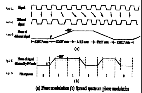
Fig. 4(a) shows a signal waveform under phase modulation. The original and
unmodulated signal 402 is shown in the top line of Fig. 4(a). The phase
modulated, or dithered,
signal 404 and its phase 406 are shown in the second and third lines of Fig.
4(a).
As shown, the phase 406 varies continuously between 0 degrees (EARLY state)
and
3o negative 180 degrees (LATE state). To prevent excessive phase change
between the two
successive phase values (EARLY state and LATE state), a SLOW state (EARLY to
LATE
transition) and a FAST state (LATE to EARLY transition) are inserted between
transitions to
and from EARLY and LATE states. In accordance with a preferred embodiment of
the present
CA 02283945 1999-09-16
WO 99/38281 PCT/US99/01246
invention, the SLOW and FAST states occupy at least 16 cycles, and the phase
change between
two successive cycles is limited to 12 degrees. Of course, within the scope of
the present
invention, the number of cycles occupied and the phase change between two
successive cycles
may vary from the particular numbers above.
Fig. 4(b) is a graph illustrating the phase 408 of the signal dithered by a
pseudo-random
code (PN sequence) 410 in accordance with a preferred embodiment of the
present invention.
For purposes of illustration, the pseudo-random sequence 410 shown starts with
the sequence
011010. Techniques for generating such pseudo-random sequences are known to
those of
ordinary skill in the pertinent art.
to When the phase modulation is controlled by a PN sequence 410 such as shown
in Fig.
4(b), the resultant power spectrum will be spread like the power spectrum in
Fig. 5(b). The
power spectrum in Fig. 5(b) has peaks with a maximum power of negative 14.6 dB
at l GHz. In
comparison, the power spectrum in Fig. 2(b) has peaks with a maximum power of
0 dB. Thus,
applying spread spectrum phase modulation in this way to the signal results in
a magnitude 14.6
15 dB reduction in peak EMI.
Although the 14.6 dB reduction from this implementation of SSPM is
substantial, it is
less than the 19.1 dB reduction from the implementation of DSSS shown in Fig.
3(c).
Nevertheless, this implementation of SSPM is advantageous over DSSS because,
unlike DSSS,
SSPM does not require a pseudo-random code generator in the receiver and so
requires simpler
2o circuitry in comparison to the circuitry for DSSS shown in Fig. 3(a).
A SSPM transmitter circuit 502 for parallel transmission of a clock signal and
multiple
data signals and for phase modulation of those clock and data signals is shown
in Fig. 5(a). The
circuit 502 includes: a clock signal source 504 for generating the clock
signal (CLK); a plurality
of data signal sources 506 for generating the multiple data signals (D0, Dl,
D2, ..., D7); a
25 control voltage source 508 for generating a control voltage (Vctrl l ); a
first voltage-controlled
delay line 510 coupled to the clock signal source 504 to receive the clock
signal and coupled to
the control voltage source 508 to receive the control voltage, the first
voltage-controlled delay
line delaying the clock signal according to the control voltage; and a
plurality of voltage-
controlled delay lines 512 coupled to the plurality of data signal sources 506
to receive the
3o multiple data signals and coupled to the control voltage source 508 to
receive the control
voltage, the plurality of voltage-controlled delay lines delaying the multiple
data signals
according to the control voltage. The output of the circuit 502 is also shown
in Fig. 5(a). The
first voltage-controlled delay line 510 outputs a dithered clock (dithered
CLK) signal 514. The
CA 02283945 1999-09-16
WO 99/38281 PCTNS99/01246
plurality of voltage-controlled delay lines 512 output dithered data signals
516.
Thus, the spread spectrum phase modulation (SSPM) technique can be applied to
both
clock and data without skew errors between data and clock as shown in Fig.
5(a). The absence
of skew errors is achieved by phase-modulating the clock and data through
voltage-controlled
delay lines (VCDLs 510 and 512) of which delays are controlled by the same
control voltage. It
is desirable that the phase difference between maximum and minimum delays
applied by the
VCDLs should be 180 degrees. This is because as the phase difference between
maximum and
minimum delays gets away from 180 degrees, the EMI reduction gets smaller
according to our
simulations.
Effect of Increased Transition Time (ITT) of Data Outputs
In order to reduce the high frequency component of the current, increasing the
transition
time (ts) is desirable. However, the slow edge rate cannot be applied to a
clock signal, so EMI
reduction on a clock signal is not expected.
t5 Since the negative 19.1 dB peak at 812.5 MHz in the case of DSSS is due
primarily to
the clock signal, no further peak reduction would occur by increasing the
transition time (ts) in
the case of DSSS. In contrast, since the negative 14.6 dB peak at 1 GHz in she
case of SSPM is
not due primarily to the clock signal, that peak will be substantially further
reduced occur by
increasing the transition time (ts) in the case of SSPM.
20 Fig. 6(a) is a graph illustrating an output voltage waveform having an
increased
transition time (ts) in accordance with a preferred embodiment of the present
invention. The
increased transition time (ts) is more distinctly shown in Fig. 6(b) which
shows the
corresponding output current waveform. The transition time (ts) for the
waveforms shown in
Figs. 6(a) and 6(b) is 5 nanoseconds (ns). In comparison, the transition time
(ts) for the
25 waveforms shown in Figs. 2(a) and 2(b) is 1 nanosecond (ns).
Fig. 6(c) is a graph illustrating the further improved reduction of the peak
values in the
power spectrum when the transition time (ts) is increased to 5 ns, and the
spread spectrum
phase modulation technique is applied in accordance with a preferred
embodiment of the present
invention. As can be seen from Fig. 6(c), the peak at 1 GHz is further reduced
to negative 31.3
3o dB.
Fig. 7 is a schematic diagram showing SSPM transmitter circuitry 700 in
accordance
with a preferred embodiment of the present invention. The transmitter
circuitry 700 includes the
phase selection circuit (PSC) 508 and a delay lock loop (DLL) 702. Both the
PSC 508 and the
CA 02283945 1999-09-16
WO 99/38281 PCTNS99/01246
DLL 702 supply control voltages to a voltage-controlled delay line (VCDL) 510.
The same or
similar circuitry would be used to supply control voltages to the other
voltage-controlled delay
lines 512.
The transmitted signal (the CLK signal in the instance shown in Fig. 7) is
modulated by
the VCDL 510. The delay applied by the VCDL 510 is controlled by two control
voltages:
Vctrl l and Vctrl2.
The generation of Vctrl l by the PSC 508 is controlled by a switching
algorithm, and
Vctrl l is used for interpolating the delay applied by the VCDL 510. For
example, the VCDL
510 generates a minimum delay (0) when Vctrll is switched to V,S. As another
example, the
VCDL 510 generates a maximum delay (T/2) when Vctrl 1 is switched to Vo.
According to a
preferred embodiment of the present invention, Vctrl l is continuously
switched from V, s to V,4,
V,3, V,,, and so on to Vo, then to V,, V,, V3, and so on to V,S, etc.
The DLL 702 generates Vctrl2 corresponding to a half period (T/2) delay
difference. The
DLL 702 includes a T/2 Phase Detector 704 with CLKO and CLKI input signals,
and UP and
DOWN output signals. The DLL 702 adjusts Vctrl2 until a rising edge of the
CLKO signal and
the falling edge of the CLK1 signal are aligned.
As Vctrl 1 is continously switched between V, 5 and Vo according to the
switching
algorithm according to a pseudo-random (PN) sequence 410, the delay applied by
the VCDL
510 varies between 0 and T/2. Furthermore, because a low-pass filter 706 is
used in the
2o generation of Vctrl l, the phase and delay vary smoothly.
Fig. 8(a) is a schematic diagram showing circuitry for a T/2 Phase Detector
704 in
accordance with a preferred embodiment of the present invention. The T/2 Phase
Detector 704
comprises a dynamic phase detector that has two input signals CLKO and CLK1
and two output
signals UP and DOWN.
For generating the UP signal output, the CLK1 signal is input to a first
inverter 802 and
to gates of a first PMOS transistor 804 and a first NMOS transistor 806. The
source of the first
PMOS transistor 804 is coupled to a supply voltage, and the drain of the first
PMOS transistor
804 is coupled to the source of a second PMOS transistor 808. The source of
the first NMOS
transistor 806 is coupled to the drain of the second PMOS transistor 808, and
the drain of the
first NMOS transistor 806 is coupled to an electrical ground. The CLKO signal
is input to a
second inverter 810.
In addition, the output of the first inverter 802 is coupled to a gate of a
third PMOS
transistor 812. The output of the second inverter 810 and the gate of the
second PMOS
7
CA 02283945 1999-09-16
WO 99/38281 PCT/US99/O1Z46
transistor 808 are coupled to a gate of a second NMOS transistor 814. The node
between the
drain of the second PMOS transistor 808 and the source of the first NMOS
transistor 806 is
coupled to the gate of a third NMOS transistor 816.
Furthermore, the source of the third PMOS transistor 812 is coupled to a
supply voltage,
and the drain of the third PMOS transistor is coupled to an input of a third
inverter 818. The
source of the second NMOS transistor 814 is also coupled to the input of the
third inverter 818,
and the drain of the second NMOS transistor 814 is coupled to the source of
the third NMOS
transistor 816. The drain of the third NMOS transistor 816 is coupled to an
electrical ground.
Finally, the output of the third inverter 818 comprises the UP output signal.
For generating the DOWN signal output, the circuitry is the same as that for
generating
the UP signal, except that the CLKO and CLK 1 input signals are reversed as
shown in the
bottom half of Fig. 8(a).
The circuitry shown in Fig. 8(a) comprises a dynamic phase detector with fewer
transistors and higher precision than prior dynamic phase detectors. Owing to
the high precision
~5 of its dynamic logic operation, the T/2 Phase Detector 704 can operate
without any phase offset.
Fig. 8(b) is a graph illustrating clock and phase detection signals in
accordance with a
preferred embodiment of the present invention. As shown in Fig. 8(b), the
widths of UP and
DOWN pulses are proportional to the phase difference of the inputs CLKO and
CLK1. Further,
there are no pulses in lock state.
2o Fig. 8(c) is a graph of phase difference vs. control voltage variation in
accordance with a
preferred embodiment of the present invention.