Note: Descriptions are shown in the official language in which they were submitted.
CA 02283953 1999-09-27
COMPACT HIGH-CAPACITY SWITCH
FIELD OF THE INVENTION
The present invention relates to digital switching
technology in general and, more particularly, to a compact, very
high-capacity switch for use in an optical transport network.
BACKGROUND OF THE INVENTION
The ever-increasing popularity of the Internet as a
vehicle for transmitting information of all sorts, including
electronic mail messages, voice conversations, photographs, data
files and live broadcasts, has led to an explosion in the volume
of digital traffic travelling on today's backbone of mainly low-
capacity (e.g., OC-3 and OC-48) links. The expression "OC-x" is
used to denote "optical carrier" and refers to a digital optical
signal having a rate of "x" times the basic rate of 51.84 Mbps,
where "x" can typically take on the values 3, 12, 48 or 192.
Thus, for example, an OC-48 signal has a rate of 2.488 Gbps,
which is approximately equal to 2.5 Gbps or 2.5 billion bits per
second.
The demand for greater network capacity brought on
largely by the advent of the information age has led to the
introduction of OC-192 links as well as a technology known as
WDM or wavelength division multiplexing. In WDM, multiple
individual optical carriers - be they OC-3 signals, OC-48
signals, OC-192 signals or any other type of signal - each
occupy distinct wavelengths of light along a span of fiber optic
cable. As multiple wavelengths are independently occupied by
various signals, the amount of information carried by a single
1
CA 02283953 1999-09-27
optical fiber can be dramatically increased with respect to the
usual case in which only a single wavelength of light is used.
It is anticipated that future transport capabilities
will be on the order of several terabits per second (Tbps, equal
to 1012 bits per second) per fiber. At the transport level, this
will likely be accommodated through the use of WDM with 100 or
more wavelengths on a single fiber, and with each wavelength
carrying an OC-192 feed (i.e., a digital optical signal at
approximately 10 Gbps). If a large number of such multi-
wavelength fibers pass through a network node, the switching
equipment at the node will be required to support capacities in
the multi-terabit-per-second range in order to provide
sufficient switching granularity for interconnecting wavelengths
from each span in a non-blocking manner. However,
conventionally available technology does not allow such
extremely high switching capacities to be achieved.
That is to say, while there has been a rapid evolution
of WDM-enabled transport technology to the point where currently
used techniques are expected to adequately support future
transport requirements, the field of switching technology has
not experienced improvements of a similar magnitude. As a
result, the telecommunications industry currently lacks access
to switches capable of cross-connecting several hundred or
several thousand multi-gigabit-per-second feeds in accordance
with an arbitrary mapping in a non-blocking way to achieve
switching capacities in the multi-terabit-per-second range.
In the quest for extremely high switching capacity,
current telecommunications service providers may suggest
extending the very concepts which have brought switching
technology to its present state. However, such concepts, which
2
CA 02283953 1999-09-27
include time-division multiplexing, time switching and space
switching, are not easily adapted to handle the switching of
multiple signals contemporaneously sharing the same transmission
medium (as is generally the case in a WDM scenario).
Furthermore, a straightforward extension of currently used
switching techniques into the terabit-per-second range leads to
central office equipment having an unacceptably high power
consumption largely as a result of a grossly impractical
physical volume.
Thus, when faced with a need to switch multiple
terabits of digital information per second inside a reasonable
volume and within reasonable limits of power consumption, it is
apparent that reliance cannot be placed upon conventionally
available switching technology.
StJNIIKARY OF THE INVENTION
The present invention provides a solution to the
above-mentioned problems inherent to currently used switching
technologies, by providing a high-capacity switch, capable of
operation in at least the multi-Tbps range, that is sufficiently
compact to fit into a single equipment shelf.
According to the invention, the implementational
difficulties associated with constructing large commutative
switches are alleviated by distributing the functionality of
various elements of a large conceptual commutative switch among
multiple circuit cards.
Thus, the invention may be summarized as a switching
unit, equipped with a plurality of port cards and a plurality of
switch cards. Each port card has at least one first M-way
3
CA 02283953 1999-09-27
commutator and a corresponding number of second M-way
commutators, wherein the total number of first M-way commutators
over all the port cards is N and wherein the total number of
second M-way commutators over all the port cards is also N.
Each switch card has at least one first N-way commutator and a
corresponding number of second N-way commutators, wherein the
total number of first N-way commutators over all the switch
cards is M and wherein the total number of second N-way
commutators over all the switch cards is also M.
Each switch card further has a unit for controllably
time switching a plurality of signals output by each first N-way
commutator and providing a plurality of switched signals to the
corresponding second N-way commutator. The mth output of the
nth first M-way commutator is connected to the nth input of the
mth first N-way commutator and wherein the nth output of the mth
second N-way commutator is connected to the mth input of the nth
second M-way commutator, for 1 <= m <= M and 1 <= n <= N.
Preferably, the M-way commutators and the N-way
commutators have harmonically related commutation step rates,
whereby the first M-way commutators on the port cards and the
first N-way commutators on the switch cards work as a P-way
commutator and whereby the second M-way commutators on the port
cards and the second N-way commutators on the switch cards work
as a P-way commutator, where P = M*N.
Preferably, the port cards are substantially parallel
to one another, wherein the switch cards are substantially
parallel to one another and wherein the normal to any port card
and the normal to any switch card are not parallel.
4
CA 02283953 1999-09-27
Preferably, the port cards are substantially parallel
to one another, wherein the switch cards are substantially
parallel to one another and wherein the port cards are
substantially orthogonal to the switch cards.
Preferably, the switching unit is further equipped
with a mid-plane connected to the port cards and to the switch
cards, wherein the connections between the first M-way
commutators and the first N-way commutators and the connections
between the second N-way commutators and the second M-way
commutators are provided by electrical paths through the mid-
plane.
Preferably, the commutators and the time switching
units cooperate to provide non-blocking time and space switching
of signals at the inputs of the first M-way commutators.
The invention may also be summarized as a port card or
a switch card as described above.
The invention may also be summarized as a compound
commutator equipped with a plurality N of first commutators
distributed among a plurality of substantially parallel first
circuit cards, each first commutator having M inputs, M outputs
and a common first commutation step rate, and a plurality M of
second commutators distributed among a plurality of
substantially parallel second circuit cards, each second
commutator having N inputs, N outputs and a common second
commutation step rate. The mth output of the nth first
commutator is connected to the nth input of the mth second
commutator for all 1 <= m <= M and 1 <= n <= N. The first and
second commutation step rates are harmonically related and the
5
CA 02283953 1999-09-27
normal to any first circuit card and the normal to any second
circuit card are not parallel.
BRIEF DESCRIPTION OF THE DRAWINGS
These and other aspects and features of the present
invention will become apparent to those of ordinary skill in the
art upon review of the following description of specific
embodiments of the invention in conjunction with the
accompanying drawings, in which:
Fig. 1A is a perspective view of a high-capacity
optical cross-connect including a set of parallel port cards
connected to a set of parallel switch cards at a mid-plane,
according to the preferred embodiment of the present invention;
Fig. 1B is a side elevational view of the optical
cross-connect of Fig. 1A;
Fig. 1C is an overhead view of the optical cross-
connect of Fig. 1A;
Fig. 1D is a perspective view of a high-capacity
optical cross-connect including two sets of parallel port cards
connected to a set of parallel switch cards by two mid-planes;
Fig. 2 is a block diagram of a port card, according to
the preferred embodiment of the present invention;
Fig. 3 is a block diagram of a 16x16 commutator;
6
CA 02283953 1999-09-27
Fig. 4A is a front elevational view of the mid-plane,
showing a plurality of connectors and high-speed data connection
areas;
Fig. 4B shows in more detail part of the mid-plane as
seen in the view of Fig. 4A;
Fig. 5 is a block diagram of a switch card, according
to the preferred embodiment of the present invention;
Fig. 6 shows an input/output diagram of a 4x4
commutator;
Fig. 7 is a functional diagram of the optical cross-
connect of Fig. 1A;
Fig. 8 shows how a partial PxN commutator can be
constructed from a PxP commutator;
Fig. 9 is a block diagram of a 4x4 commutator;
Fig. 10 is a block diagram of a PxP commutator
distributed as N MxM commutators connected to M NxN commutators,
where P = M*N;
Fig. 11 is a block diagram of a control processor
card;
Fig. 12 shows a micro-electro-mechanical device for
protecting traffic going to and coming from a failed port card;
Fig. 13 is a perspective view of a high-capacity
optical cross-connect including a sets of parallel port cards
7
CA 02283953 1999-09-27
connected to a set of parallel switch cards without the
intermediary of a mid-plane;
Fig. 14 shows a block diagram of a two-by-two space
time switch; and
Fig. 15 shows how an orthogonal interconnection of
commutators in Fig. 10 simplifies the wiring arrangement between
the sets of commutators.
DETAILED DESCRIPTION OF THE PREFERRED EMBODIMENT
Before the present invention is described in any
detail, it is useful to introduce the concept of a commutator
and that of a commutative switch, which are used extensively
throughout the remainder of the detailed description. An MxM
(or "M-way") commutator is an M-input, M-output circuit that
transfers the data arriving on each of its M inputs over to each
one of its M outputs for 1/Mth of the time in a repetitive
cyclical manner.
With reference to Fig. 9, there is shown in more
detail one possible way in which a four-input, four-output
commutator 900 can be built. Similar concepts will apply to
building a larger commutator. In the case of 4x4 commutator
900, four inputs A, B, C, D lead to two 2x2 switches 226C1,
226C2 and four outputs E, F, G, H are taken from another pair of
2x2 switches 226D1, 226D2. One output of switch 226C1 is
connected to one input of switch 226D1, the other output of
switch 226C1 is connected to one input of switch 226D2, one
output of switch 226C2 is connected to the other input of switch
226D1 and the other output of switch 226C2 is connected to the
other input of switch 226D2.
8
CA 02283953 1999-09-27
Each individual switch is programmed to toggle between
a straight-through mapping and a cross-over mapping at evenly
spaced time intervals. The rate of toggling an individual
switch depends on the position of the switch in the commutator.
Specifically, switches 226C1, 226C2 are caused to toggle (step)
at a rate known as the commutation step rate (CSR), while
switches 226D1, 226D2 are caused to toggle at half this rate.
As a result, the exact same switching cycle repeats every four
steps. The frequency at which the entire cycle repeats itself
is known as the commutation cycle rate (CCR) and, in this case,
is equal to CSR/4.
Operation of the commutator 900 is now described with
reference to Fig. 6, where data elements present at each of the
four inputs A, B, C, D is shown as being indexed by a time
subscript which begins at 0 seconds (on the far right) and
increases towards the left on a per-second basis. It is assumed
for the purposes of illustration that a new data element arrives
every second and that switches 226C1 and 226C2 are toggled every
two seconds (i.e., the commutator 900 has a CSR of % seconds-1).
This leads to a cycle time of 4*2 = 8 seconds. Also, it is
assumed that the data collected at the outputs E, F, G, H
suffers no delay as it passes through the commutator 900.
During the first two seconds, outputs E, F, G and H
contain data from inputs A, C, B and D, respectively. After 2
seconds, switches 226C1 and 226C2 toggle and outputs E, F, G and
H are respectively connected to inputs B, D, A and C. This is
the state of affairs for the next two seconds, at which point
switches 226C1 and 226C2 switch back to their initial mappings.
In addition, at this point half-way through the cycle, switches
226D1 and 226D2 toggle their respective mappings. Thus, during
9
CA 02283953 1999-09-27
the next two seconds, the data at outputs E, F, G and H comes
from inputs C, A, D and B, respectively. Two seconds later,
switches 226C1 and 226C2 are again toggled, and outputs E, F, G
and H contain data from inputs D, B, C and A, respectively.
This mapping remains in place until 8 seconds have gone by, at
which point the entire cycle is repeated.
Thus, it is seen that the effect of the commutator 900
is to distribute data from each of the 4 inputs among the 4
outputs during one-quarter of the time. The order in which the
inputs A, B, C, D appear on the outputs E, F, G, H can be
changed by changing the toggling rate associated with the
various switches. Those skilled in the art will appreciate that
the original input data streams A, B, C, D can be recovered by
passing the commutated output data streams E, F, G, H through an
identical commutator running at the same CSR and CCR, except
where the outputs of the second commutator are used as inputs
and vice versa.
Reference is now made to Fig. 3, which shows in more
detail one possible way in which a sixteen-input, sixteen-output
commutator 930 can be implemented. Of course, there are many
other ways of building a commutator. The sixteen input ports
930A-930P correspond in actuality to a totality of input ports
belonging to a first set of eight two-by-two switches 226A1-8,
while the sixteen output ports 930A', 930B'-930P' correspond in
actuality to a totality of output ports belonging to a fourth
set of eight two-by-two switches 226D1-8. Between the first and
fourth sets of switches lie second and third sets of eight two-
by-two switches, respectively shown at 226B1-8 and 226C1-8 in
Fig. 3.
CA 02283953 1999-09-27
The four sets of eight two-by-two switches 226A1-8,
226B1-8, 226C1-8, 226D1-8 are interconnected as follows. The
outputs of switch 226A1 are connected to the inputs of switches
226B1 and 226B5, the outputs of switch 226A2 are connected to
the inputs of switches 226B2 and 226B6, the outputs of switch
226A3 are connected to the inputs of switches 226B3 and 226B7
and the outputs of switch 226A4 are connected to the inputs of
switches 226B4 and 226B8. Switches 226A5 through 226A8 are
connected to switches 226B1 through 226B8 in a similar fashion.
Next, the outputs of switch 226B1 are connected to the
inputs of switches 226C1 and 226C3, the outputs of switch 226B2
are connected to the inputs of switches 226C2 and 226C4, the
outputs of switch 226B3 are connected to the inputs of switches
226C3 and 226C1 and the outputs of switch 226B4 are connected to
the inputs of switches 226C4 and 226C2. An identical connection
pattern exists among switches 226B5 through 226B8 and switches
226C5 through 226C8.
Finally, one output of switch 226C1 is connected to
one input of switch 226D1, the other output of switch 226C1 is
connected to one input of switch 226D2, one output of switch
226C2 is connected to the other input of switch 226D1 and the
other output of switch 226C2 is connected to the other input of
switch 226D2. An identical connection pattern exists between
pairs of switches 226C3, 226C4 and 226D2, 226D4, between pairs
of switches 226C5, 226C6 and 226D5, 226D6 and between pairs of
switches 226C7, 226C8 and 226D7, 226D8.
Each individual switch is programmed to toggle between
a straight-through mapping and a cross-over mapping at evenly
spaced time intervals. A command to toggle each switch is
received from a common control unit (not shown) via control
11
CA 02283953 1999-09-27
lines 228A, 228B, 228C, 228D. The rate of toggling an
individual switch depends on the set to which the switch
belongs. Specifically, switches 226D1-8 in the fourth set are
programmed to switch at a rate known as the commutation step
rate (CSR). Switches in the third, second and first sets are
programmed to switch at rates of CSR/2, CSR/4 and CSR/8,
respectively. As a result, the exact same switching cycle
repeats at intervals that are 16 times as long as the interval
of a single step. The frequency at which the entire cycle
repeats itself, known as the commutation cycle rate (CCR), is
equal to CSR/16 ore one-sixteenth of the commutation step rate.
Without going into more detail, it will be appreciated
that the effect of the commutator 930 is to distribute data from
each of the 16 inputs 930A-930P among the 16 outputs 930A'-930P'
during one-sixteenth of the time. Those skilled in the art will
also appreciate that the original input data streams can be
recovered by passing the commutated output data streams through
an identical commutator running at the same CSR and CCR, except
where the outputs of the second commutator are used as inputs
and vice versa.
Reference is now had to U.S. Patent 4,450,557 issued
to E. Munter, assigned to the assignee of the present invention
and incorporated by reference herein in its entirety. U.S.
Patent 4,450,557 describes a manner of achieving non-blocking
time and space switching of a plurality of frame-based input
signals.
Specifically, with reference to Fig. 14, a switch 1400
according to U.S. Patent 4,450,557 has 2 inputs S, T and 2
outputs U, V. The switch 1400 comprises two sets of switches
1410, 1415 flanking either side of set of data memories 1420.
12
CA 02283953 1999-09-27
Another set of switches 1430 is connected between a pair of
connection memories 1440 and respective data memories 1420. The
rate of switching the switches 1410, 1415, 1430 is the same and
is fixed.
The connection memories 1440 contain a desired time
slot interchange map for each output U, V. Because of the
interaction of switches 1410, 1415, 1430, and because the
specific connection memory 1440 used to read from a given data
memory 1420 varies as a function of time, the time slot
interchange maps stored by the connection memories 1440 can be
used to achieve non-blocking time and space switching.
In the general case where there are more than two
inputs and more than two outputs, non-blocking time and space
switching can be conceptually achieved by providing commutators
instead of switches 1410, 1415, 1430. However, in the case of a
very large and high-capacity switch, a straightforward extension
of the concepts introduced in U.S. Patent 4,450,557 leads to a
grossly impractical realization of a commutative switch. For
example, when it is desired to build a PxP non-blocking switch,
the required size of the commutators on either side of the data
memory bank is PxP. Thus, if it is desired to build a 2.56 Tbps
switch capable of accepting inputs of 10 Gbps per input, then P
= 2.56 Tbps / 10 Gbps = 256 and the required commutator size is
therefore 256x256.
However, using currently available technology, it is
virtually impossible to build commutators of this size. Simply
by observing the increase in complexity brought on by moving
from commutator 900 (in Fig. 9) to commutator 930 (in Fig. 3),
it can be understood that moving from a 16x16 commutator to a
256x256 commutator requires an excessively complex wiring
13
CA 02283953 1999-09-27
pattern. Furthermore, it is highly impractical to construct
integral devices with 256 high-speed inputs and 256 high-speed
outputs.
According to the invention, the implementational
difficulties associated with constructing large commutative
switches are alleviated by distributing the functionality of
various elements of the switch among multiple circuit cards.
To begin with, large commutators are built from
smaller ones using a procedure such as the following, which
applies to the construction of a PxP commutator:
1) Factorize P into M and N;
2) Assemble a first group of N commutators (each of
size M x M) and a second group of M commutators
(each of size N x N);
3) Connect the mth output of the nth commutator in the
first group to the nth input of the mth commutator in
the second group, where 1 S m S M and 1 S n S N; and
4) Set the CSR for the commutators in one group equal
to the CCR of the commutators in the other group.
With reference to Fig. 10, there is shown a PxP
commutator 1000 constructed in accordance with the above
procedure. Specifically, P = M*N and there are N commutators
lOlOA-1010N of size MxM (i.e., M-way commutators) connected to M
commutators 1020A-1020M of size NxN (i.e., N-way commutators).
The MxM commutators 1010A-1010N have a CSR denoted CSRM and the
NxN commutators 1020A-1020M have a CSR denoted CSRN. By
14
CA 02283953 1999-09-27
harmonically relating CSRM and CSRN, commutator 1000 can be made
to behave as a PxP commutator.
It is noted in Fig. 10 that if the two sets of
commutators 1010A-1010N, 1020A-1020M lie in the same plane, then
the interconnect region between the commutators exhibits a
complicated wiring pattern. It has been recognized by the
inventors that this wiring pattern can be significantly
simplified by placing the commutators in one set in a different
plane than the commutators in the other set. For example, the
desired effect can be achieved by placing commutators 1020A-
1020M orthogonally with respect to commutators 1010A-lOlON, as
shown in Fig. 15. It is seen that the wiring pattern is greatly
simplified, as each connection between two commutators is a
straight-through connection and can be made to have
substantially the same length, leading to improved conditions
for signal propagation.
Thus, it has been shown how a PxP commutator (where P
M*N) can be divided into a set of N commutators connected to a
set of M commutators. This fact is used to partition a large
conceptual commutative switch into workable elements. For
example, with reference to Fig. 7, there are shown various
functional elements of a large commutative switch 700 according
to the preferred embodiment of the present invention. Also
shown is the manner in which the functional elements of the
switch 700 are physically distributed among a set of circuit
cards 201A-K, 202A-K, 300A-300L.
Functionally, the P-input, P-output switch 700 consists
mainly of two large distributed PxP commutators 740, 745
flanking either side of a large distributed time switch 750.
Commutator 740 is built from N commutators 230A-230N (each of
CA 02283953 1999-09-27
size MxM) and M commutators 320A-320M (each of size NxN)
according to the above described method. Similarly, commutator
745 has been built from M commutators 330A-330M (each of size
NxN) and N commutators 235A-235N (each of size MxM) according to
the above described method. The interconnect pattern within
each of the compound commutators 740, 745 is greatly simplified
by providing orthogonality between the circuit cards comprising
commutators 230A-230N and those comprising commutators 320A-
320M, and between the circuit cards comprising commutators 235A-
235N and those comprising commutators 330A-330M.
The commutators 740, 745 and the time switch 750 are
distributed among K receive port cards 202A-202K, K transmit
port cards 201A-201K and L switch cards 300A-300L. In the
preferred embodiment, K is equal to N and L is equal to M/2. Of
course, it is to be understood that the number of port cards and
the number of switch cards is arbitrary and may depend on the
amount of processing required to support the components on each
card.
Each of the receive port cards 202A-202K is equipped
with a respective one of the commutators 230A-230N and a
respective one of a plurality of receive processing sections
760A-760K connected to the respective commutator. Similarly,
each of the transmit port cards 201A-201K is equipped with a
respective one of the commutators 235A-235N and a respective one
of a plurality of receive processing sections 765A-765K
connected to the respective commutator.
Also, because L = M/2, each of the switch cards 300A-
300L is equipped with two of the commutators 320A-320M, two of
the commutators 330A-330M and a common processing section 730
connected to each commutator.
16
CA 02283953 1999-09-27
It is apparent from Fig. 7 that the interconnect region
existing between sets of commutators 230A-N and 320A-M is
complex. If an attempt is made at building a backplane through
which receive port cards 202A-202K can be connected to switch
cards 300A-300L, then such a backplane would have to be 16
traffic layers thick (leading to a thickness of approximately 48
physical layers) in order to accommodate the complex
interconnection requirements. Such backplanes are not only
expensive to build, but take up a sizable physical volume and
must be handled with extreme care. A similar scenario arises if
the switch cards 300A-300L are to be connected to the transmit
port cards 201A-201K via a standard backplane.
In order to alleviate such interconnection
difficulties, the invention exploits the advantages of
orthogonality described earlier with respect to Fig. 15 and
provides a mid-plane architecture which is now described with
reference to Figs. 1A through 1D.
Preferably, each of the receive port cards 202A-202K
is grouped together with a respective one of the transmit port
cards 201A-201K into a single universal (combined transmit and
receive) port card that provides both input and output
functionality. Accordingly, Figs. 1A, 1B and 1C depict a
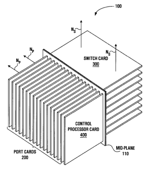
switching unit 100 in accordance with the preferred embodiment
of the present invention, where one parallel set of universal
port cards 200A-200K (herein after referred to simply as "port
cards") is shown connected to a parallel set of switch cards
300A-300L via a single mid-plane 110. The switching unit 100
also comprises at one or more control processor cards 400 which
could be connected to the mid-plane 110 in any suitable way,
17
CA 02283953 1999-09-27
such as in parallel with the port cards 200A-200K as shown in
Fig. 1A.
Alternatively, Fig. 1D shows an embodiment in which the
switch cards 300A-300L are connected to the receive port cards
202A-202K via a first mid-plane 110 and are connected to the
transmit port cards 201A-201K via a second mid-plane 111. Each
of the switch cards 300A-300L is tilted at 90 degrees with
respect to the plane of each of the receive port cards 202A-202K
and transmit port cards 201A-201K. The first mid-plane 110
provides an electrical connection between each of the receive
port cards 202A-202K and all of the switch cards 300A-300L,
while the second mid-plane 111 provides an electrical connection
between each of the switch cards 300A-300L and all of the
transmit port cards 201A-201K.
The switching unit 100 may also be referred to as an
optical cross-connect (OXC), since it provides the capacity and
granularity to interconnect entire payloads of optical bit
streams. These optical bit streams enter and exit the OXC 100
through processing sections 760A-K, 765A-K in the port cards
200A-200K, which were briefly touched upon earlier with
reference to Fig. 7 and will be described in further detail
herein below. The optical bit streams are exchanged (via
optical fiber) between the OXC 100 and central office equipment
in one or more locations.
By way of the mid-plane 110, each of the port cards
200A-200K has a high-speed connection to all of the switch cards
300A-300L and each of the switch cards 300A-300L has a high-
speed connection to all of the port cards 200A-200K. This can
be achieved by orienting the port cards 200A-200K and the switch
cards 300A-300L in different directions and providing a simple
18
CA 02283953 1999-09-27
electrical interconnect mapping through the mid-plane 110.
Using a more general formulation, a simple interconnect mapping
can be used as long as the normal orientation of the port cards
200A-200K (indicated by arrows NP) is not parallel to the normal
orientation of the switch cards 300A-300L (indicated by arrows
Ns).
A preferred orientation of the port cards 200A-200K
relative to the switch cards 300A-300L is shown in Figs. lA, 1B
and 1C, where NP is at right angles to Ns. Alternatively, the
port cards and switch cards could meet each other obliquely
rather than orthogonally, in which case the angle between Ns and
NP would be greater or less than 90 degrees. In either case, the
interconnect problem of Fig. 10 is solved, leading to an
interconnect pattern more similar to that in Fig. 15.
It is to be understood that any suitable mechanical
structure (such as a chassis and a set of card guides) could be
used for maintaining the port cards 200A-200K and the switch
cards 300A-300L substantially fixed in relation to each other.
Preferably, the chosen support structure will allow the port
cards 200A-200K and the switch cards 300A-300L to be removed by
an operator if such cards are found defective or for any other
reason.
The mid-plane 110 serves two functions. Firstly, it
allows for electrical contact between each port card and all
switch cards, and between each switch card and all port cards.
This can be achieved merely by providing an opening through
which complementary pins on the port card switch cards can mate.
Alternatively, this can be achieved by providing an electrical
pathway between an arrangement of conductive pins on a port side
19
CA 02283953 1999-09-27
110P and a similar arrangement of conductive pins on a switch
side 110S.
Specifically, with reference now to Fig. 4A, in which
is shown in greater detail the physical layout of the mid-plane
110 as viewed from the port side 110P, the port side 110P is
seen to comprise a number of connectors (shown in solid outline
at 120A-120K) for accommodating respective port cards. Shown in
dotted outline at 150A-150L is a similar but perpendicularly
oriented arrangement of connectors for accommodating respective
switch cards on the switch side 110S of the mid-plane 110. Of
course, if the port cards 200A-200K are obliquely arranged
relative to the switch cards 300A-300L, then the pairs of
connectors 120i, 150j will be obliquely oriented for 1 <= i <= k
and 1 <= j <= L.
In addition, a connector 180 for connecting the
control processor card 400 to the mid-plane 110 is shown on the
port side 110P. Of course, the connector 180 could be located
on the switch side 110S and it could be oriented differently
(i.e., not in parallel with any of connectors 120A-120K or 150A-
150L). Furthermore, there may additional connectors for
connecting duplicate control processor cards (in case of failure
of control processor card 400).
Each of the connectors 120A-120K consists of a
plurality of high-speed data connection areas 130, one for each
switch card. Thus, in the case where there are K port cards and
L switch cards in the OXC 100, the high-speed data connection
areas 130 will be laid out in a matrix structure having K
columns of L rows. As shown in Fig. 4B, each high-speed data
connection area 130 has an array of one or more high-speed data
pins 140. Between the high-speed data connection areas 130 are
CA 02283953 1999-09-27
located "auxiliary" pins 145 which could be used for power,
grounding, timing and control.
The term "pin" is used loosely so as to designate any
electrical contact point, which includes balanced (single-ended)
and differential conductors, such as copper pins and vias,
surface mounted pins, through-board pins, double-sided pins et
cetera. Also, the term "pin" is used indiscriminately to
generically designate both actual protruding pins and
receptacles for complementarily mating with such protrusions.
Similarly, each of the connectors 150A-150L consists
of a plurality of high-speed data connection areas 160, one for
each port card. Thus, in the case where there are K port cards
and L switch cards in the OXC 100, the high-speed data
connection areas 160 will be laid out in a matrix structure
having L rows of K columns. As shown in Fig. 4B, each high-
speed data connection area 160 has an array of one or more high-
speed data pins 170. Between the high-speed data connection
areas 160 are located auxiliary pins 175 which could be used for
power, grounding, timing and control.
The mid-plane 110 provides electrical contact between
the high-speed data pins 140 in each high-speed data connection
area 130 on the port side 110P and respective high-speed data
pins 170 in a corresponding high-speed data connection area 160
on the switch side 110S. Since the number of high-speed data
connection areas (and the number of high-speed data pins per
high-speed data connection area) on both sides of the mid-plane
is the same, there is a one-to-one correspondence between the
high-speed data connection areas (and the high-speed data pins)
on either side.
21
CA 02283953 1999-09-27
In order to establish an electrical connection between
two high-speed data pins (one on either side of the mid-plane
110), any suitable technique may be used. For example, the two
high-speed data pins in question could be connected by
electrical vias and pathways through one or more printed circuit
board layers in the mid-plane 110. In general, the shorter the
path, the less the propagation delay and distortion, and the
higher the performance.
Also, it is noted from Fig. 4B that although
connection areas 130, 160 intersect, the high-speed data pins
140 on one side of the mid-plane are slightly offset from the
data pins 170 on the other side. This can be done to allow
conventional pins mounted on one side of the mid-plane 110 to
run all the way through the mid-plane and emerge on the other
side. Of course, those skilled in the art will appreciate that
the pins on opposite sides of the mid-plane may overlap if
surface-mounting technology is used. Alternatively, one ling
pin can be used to mate with both the port card and the switch
card.
The second function of the mid-plane 110 is to enable
the provision of "auxiliary" functions such as power, grounding,
timing and control. Therefore, the mid-plane 110 does not
provide electrical direct contact between the auxiliary pins 145
on the port side 110P and the auxiliary pins 175 on the switch
side 110S. Rather, the auxiliary pins associated with each of
the connectors 120A-120K, 150A-150L are electrically connected
(via pathways through one or more conductive layers in the mid-
plane) to either the control processor card 400 or the central
office.
22
CA 02283953 1999-09-27
Auxiliary functions involving the central office
include power and grounding. To provide power to the circuit
cards in the OXC 100, a separate power line could be provided
from the central office to a single area on one side of the mid-
plane 110, which area is then electrically connected to an
auxiliary pin on each of the connectors 120A-120K, 150A-150L.
To provide grounding of the circuit cards in the OXC 100, one
auxiliary pin from each of the connectors 120A-120K, 150A-150L
could lead to a common area on the mid-plane 110 which could be
connected to a local ground reference or to a ground reference
shared with the central office.
The remaining functions (e.g., timing and control)
involve the control processor card 400, which is now described
in further detail with reference to Fig. 11. The control
processor card 400 is constructed so as to mate with a connector
180 on the mid-plane which, in the preferred embodiment, is
located on the port side 110P of the mid-plane 110 and is
parallel to connectors 120A-120K.
With reference to Fig. 11, therefore, the control
processor card 400 accepts extracted clock signals from the mid-
plane via signal lines 1115A-1115K. Each of the signal lines
1115A-1115K carries a clock signal extracted by a respective one
of the port cards 200A-200K and delivered to the mid-plane via
one of the auxiliary pins belonging to the connector associated
with the respective port card.
The extracted clock signals on signal lines 1115A-
1115K (arriving from the port cards via pins such as pin 212E on
port card 200 in Fig. 2) are fed to a selector 1120 which allows
only one of these extracted clock signals to pass through to
signal line 1125 in response to a control signal received from a
23
CA 02283953 1999-09-27
central processor 1110 along a control line 1105. The selected
extracted clock signal carried by signal line 1125 is fed to a
clock recovery unit 1130. The clock recovery unit 1130
comprises circuitry such as a phase-locked loop (PLL) for
locking the OXC clock source to the precise frequency of the
network reference clock signal.
The precise timing reference produced by the clock
recovery unit 1130 is used as a high-speed clock for
synchronizing the entire OXC 100. This high-speed clock is fed
to a clock driver 1140 along a signal line 1135. The driver
1140 comprises circuitry for outputting the high-speed clock to
the mid-plane along individual clock lines 1145, one for each
circuit card (i.e., one high-speed clock signal is destined for
each of the port card 200A-200K and each of the switch cards
300A-300L).
Thus, a centralized source (e.g., the clock recovery
unit 1130) distributes a clock signal to one auxiliary pin in
each of the connectors 120A-120K, 150A-150K along an individual
point-to-point electrical pathway through the mid-plane 110. To
ensure accurate timing distribution, the pathways should all be
designed to have the same length irrespective of the distance
between the control processor card 400 and the target auxiliary
pin on each of the connectors 120A-120K, 150A-150L. This can be
achieved by using an indirect folded electrical path for
connectors associated with closer cards and choosing a more
direct pathway for connectors associated with more distant
cards.
In addition, the control processor exchanges control
information with one or more auxiliary pins on each of the
connectors 120A-120K, 150A-150L. This control information is
24
CA 02283953 1999-09-27
preferably exchanged at a speed that is suitable for the
interconnection of a central processor to a number of dependent
entities, which is usually substantially lower than the speed at
which the extracted clock signals or the high-speed clock signal
are exchanged. Thus, a serial or parallel bus architecture
(e.g., bus 1160) can be used. The bus is connected to central
processor 1110.
The central processor 1110 is preferably a micro-
processor running an algorithm. This algorithm contains a
portion for selecting the selected extracted clock signal which
could be based on the precise timing reference produced by the
clock recovery unit 1130. Another portion of the algorithm is
concerned with processing the control information received from
the circuit cards along the bus 1160 and generating control
information for transmission to the various circuit cards. The
central processor 1110 is preferably connected to a port 1150
leading to the central office, where a higher level of
processing may take place.
Reference is now made to Fig. 2, which shows a generic
port card 200 according to the preferred embodiment of the
invention, equipped with a connector 210, a pair of MxM
commutators 230, 235 and a pair of processing sections 760, 765
connected to commutators 230, 235, respectively. Port card 200
structurally represents any of the port cards 200A-200K in the
OXC 100.
Connector 210 is disposed along an edge 201 of the
port card 200 and comprises L high-speed data connection areas
210A-210L, one for each switch card. The high-speed data
connection areas 210A-210L each comprise a set of high-speed
data pins for communicating high-speed data with respective
CA 02283953 1999-09-27
high-speed data pins 140 belonging to a connection area 130 on
the port side 110P of the mid-plane 110. Also, connector 210
comprises a plurality of auxiliary pins 212C, 212T, 212G, 212P
and 212E which are interspersed among the high-speed connection
areas 210A-212L.
Generally, the high-speed data pins in each high-speed
connection area transport an aggregate bandwidth of R*K/L Gbps,
where R is the bandwidth of each of P signals being processed by
commutators 740, 745 (in Fig. 7), K is the number of port cards
and L is the number of switch cards. A possible value for R is
10, corresponding to an OC-192 signal, although the invention
will work for any value of R. Without loss of generality, it
can be assumed that a single high-speed data pin can carry one
of P signals at R Gbps and therefore the number of pins per
high-speed connection area is K/L in each direction of
communication (to and from the mid-plane 110).
Thus, if there are twice as many port cards as switch
cards (as shown in the illustrated embodiment), then the number
of high-speed data pins per high-speed connection area will be
four. Therefore, high-speed data connection area 210A in
particular is shown to comprise four high-speed data pins, 211A,
212A, 213A, 214A, among which pins 211A and 212A transport high-
speed data from commutator 230 to the mid-plane 110 and pins
213A and 214A carry high-speed data from the mid-plane to
commutator 235.
Preferably, each high-speed data pin 211A, 212A, 213A,
214A is a single pin carrying data at R Gbps (e.g., 10 Gbps) or
is a group of Q pins carrying R/Q Gbps per pin.
26
CA 02283953 1999-09-27
Connector 210 is matched with a corresponding one of
the connectors 120A-120K on the port side 110P of the mid-plane
110. In fact, each of the pins associated with connector 210
are aligned with respective pins in the corresponding connector
on the port side 110P of the mid-plane 110 and are provided with
a complementary mating assembly. Thus, when port card 200 is
connected to the port side 110P of the mid-plane, the high-speed
data pins associated with each connection area 210A-210L
electrically mate with the corresponding set of high-speed data
pins in the corresponding connection areas 130 belonging to the
corresponding port-side connector, while the auxiliary pins from
connector 210 electrically mate with the auxiliary pins
belonging to the corresponding port-side connector.
In order to ensure good electrical contact between a
pair of connectors (connector 210 on the port card 200 and a
corresponding connector on the port side 110P of the mid-plane
110), it is possible to rely on a frictional contact force.
However, in the case where several hundred pins may be used, it
is preferable to use known ZIF (zero insertion force) connectors
which provide a means for applying a contact force after
physical positioning of the card and, even more importantly, a
means for removing the contact force prior to physical movement
of the card.
At the other end of the port card 200 is provided an
optical receive circuit 270 for accepting a plurality of optical
signals from a set of external input optical fibers,
collectively denoted by reference numeral 280. The data rate of
the signal arriving on each of the external input optical fibers
280 is matched to the commutator port capacity, either by
straight mapping or by a synchronized multiplexer or
demultiplexer. Collectively, the bandwidth of all the signals
27
CA 02283953 1999-09-27
entering the optical receive circuit should equal M*R Gbps,
where M is the size of the NxN commutator in the port card and R
is the rate handled by each pin 211A, 212A, 213A, 214A. Thus,
there may be one or more external input fibers 280 entering the
optical receive circuit 270.
The optical receive circuit 270 (which could be
multiple individual optical receive circuits) comprises opto-
electronic conversion circuitry for converting the optical
signals arriving on external input optical fiber(s) 280 into a
plurality of digital electronic signals which are fed to a bank
of processing and conditioning units 250A-250X along respective
signal lines 260A-260X. If the incoming optical signals carry
data at rates that are higher than R Gbps, then the optical
receive circuitry 270 preferably comprises additional circuitry
for synchronously demultiplexing the signals into individual
electronic signals having a rate of R Gbps. If the incoming
optical signals carry data at rates that less than R Gbps, then
the optical receive circuitry 270 preferably comprises
additional circuitry for synchronously combining multiple the
signals into individual electronic signals having a rate of R
Gbps.
Each of the processing and conditioning units 250A-
250X preferably comprises circuitry for monitoring the quality
of the respective signal received from the optical receive
circuit 270. If the incoming signal is a SONET signal, for
example, then this signal will consist of frames and each frame
will generally have a header portion reserved for carrying
control information. In this case, each of the processing and
conditioning units 250A-250X will preferably comprise circuitry
such as a frame find unit (for locating the boundaries of
incoming frames and extracting a clock) and a processor (for
28
CA 02283953 1999-09-27
processing the information in the header of each frame).
Similar processing circuitry could be provided for switching
entire 10-gigabit Ethernet or 1-Gigabit Ethernet signals (as
opposed to routing individual frames).
Any control information to be sent by the processing
and conditioning units 250A-250X to the control processor card
400 can be exchanged via a control bus 290, which could be a
serial bus or a parallel bus. For example, in the particular
case of processing and conditioning unit 250A, signal quality
information could be output onto control bus 290 via a control
link 291. Also, in order to allow processing and conditioning
unit 250A to be accessed by an external operator (e.g., during
re-programming), access could be provided by a control link 298
emanating from the same control bus 290. Control bus 290 is
connected to auxiliary pin 212C, which is designed to mate with
a complementary auxiliary pin on the port side of the mid-plane
which is electrically connected to the control bus 1160 on the
control processor card 400.
Furthermore, the clock signal extracted by one or more
of the processing and conditioning units (in this case
processing and conditioning unit 250A) could be used as the
extracted clock signal which is connected to auxiliary pin 212E
or multiples thereof. Alternatively, each of the processing and
conditioning units 250A-250X could output an extracted clock
signal to a selector, the output of which would be connected to
auxiliary pin 212E. Auxiliary pin 212E is designed to mate with
a complementary pin on the port side of the mid-plane which is
electrically connected to a respective one of the signal lines
1115A-1115K leading to the selector 1120 in the control
processor card 400. Thus, an extracted clock is fed to the
29
CA 02283953 1999-09-27
clock recovery circuit 1130 on the control processor card 400
for use as a reference clock.
The set of processing and conditioning units 250A-250X
is connected to via an optional TDM mux 240 to a set of input
ports 230A-230M of MxM commutator 230. The optional TDM mux 240
is present in order to provide the capability to multiplex
several signals at a lower rate (less than R Gbps) into a signal
having a rate of R Gbps. Not shown is an optional
demultiplexer, which would be used to separate a higher-
bandwidth signal into multiple individual signals of bandwidth R
Gbps each.
In any event, there will be M signals (at R Gbps each)
arriving at the commutator 230. Commutator 230 is an MxM
commutator with a commutation step rate that is controllable by
a sequencing signal arriving on a sequencing signal line 297.
The sequencing signal is output by a sequencing unit 296. The
sequencing unit 296 basically consists of clock divider
circuitry for dividing a high-speed clock received from
auxiliary pin 212T. Auxiliary pin 212T is designed to mate with
a complementary pin on the port side of the mid-plane which is
electrically connected to a respective one of the clock lines
1145 leading from the clock driver 1140 in the control processor
card 400.
In synchronism with the sequencing signal, commutator
230 sequentially switches its M inputs over to M outputs 230A'-
230M' which are respectively connected to a plurality of signal
lines 220A-220M. Signal lines 220A-220M then lead to respective
high-speed data pins on the various high-speed connection areas
210A-lOL on connector 210. In the illustrated embodiment, there
are L = M/2 high-speed data connection areas 210A-210L but M
CA 02283953 1999-09-27
signal lines 220A-220M. Thus, two signal lines are connected to
each one of the high-speed data connection areas 210A-210L.
In the reverse direction, commutator 235 has M inputs,
among which each pair is connected to a pair of high-speed data
pins in each of the high-speed data connection areas 210A-210L.
Commutator 235 is identical to commutator 230 but because
commutator 235 handles signals which have already been switched
by the switch cards 300A-300L, it performs the inverse function
of commutator 230 and therefore, from a sequencing perspective,
it is connected backwards so as to reintegrate the slices of
data. However, the CSR and CCR remain the same and commutator
235 switches of signals present at its M inputs 235A-235M over
to M outputs 235M'-235M' in a repetitive cyclical manner in
accordance with the sequencing signal received along sequencing
signal line 297.
The output ports 235A'-235M' of commutator 235 are
connected to a respective plurality of processing and
conditioning units 255A-255X via an optional demux 245. if
used, the demux 245 serves to separate one high-capacity signal
exiting the commutator 235 at R Gbps into multiple lower-
capacity signals.
Processing and conditioning units 245A-245X may
comprise circuitry for inserting control information into the
header of selected SONET or 10-gigabit Ethernet frames received
from the demux 245. This control information could be provided
via control links sharing a control bus. By way of example,
Fig. 2 shows processing and conditioning unit 255A as being
connected to control bus 290 via an input control link 294 and
an output control link 295.
31
CA 02283953 1999-09-27
Processing and conditioning units 255A-255P are
connected to an optical transmit circuit 275 by a respective
plurality of signal lines 265A-265X. The optical transmit
circuit 275 comprises circuitry for converting the digital
electronic signals received from the processing and conditioning
units into respective single-wavelength optical signals.
Because pins 213A and 214A carry signals at R Gbps, the totality
of optical signals output by the optical transmit circuit 275
(or multiple such circuits) will have an aggregate capacity of
M*R Gbps. The single-wavelength optical signals generated by
the optical transmit circuit 275 is output onto a respective set
of external output optical fibers 285.
Thus, when the example port card 200 having MxM
commutators 230, 235 is connected to the port side 110P of the
mid-plane 110, commutator 230 will provide L sets of M/L high-
speed data signals at R Gbps each, with each set of signals
being transmitted to a respective one of the L switch cards
300A-300L via the mid-plane 110, while commutator 235 will
expect to receive L sets of M/L high-speed data signals at R
Gbps each, one set from each switch card via the mid-plane 110.
Straight-through high-speed data connections from the port cards
to the switch cards are provided by the mid-plane 110.
Reference is now made to Fig. 5, which shows a generic
switch card 300 in accordance with the preferred embodiment of
the present invention. Switch card 300 structurally represents
any of the switch cards 300A-300L in the OXC 100, but can be
taken to be switch card 300A in Fig. 7 for purposes of
illustration. Switch card 300 is equipped with a connector 310,
an NxN commutator 320A, an NxN commutator 330A and a processing
section 730 connected to the commutators 320A, 330A. It is
noted that commutators 330A and 330B - although shown in Fig. 7
32
CA 02283953 1999-09-27
- are not illustrated in Fig. 5 in order to avoid unnecessarily
cluttering the Figure. Nevertheless, their existence is assumed
and they are also assumed to be connected to processing section
730.
Connector 310 is disposed along an edge 301 of the
switch card 300 and comprises K high-speed data connection areas
310A-310K, one for each port card. The high-speed data
connection areas 310A-310K each comprise a set of high-speed
data pins for communicating high-speed data with respective
high-speed data pins 170 belonging to a connection area 160 on
the switch side 110S of the mid-plane 110. Also, connector 310
comprises a plurality of auxiliary pins 312C, 312T, 312G and
312P which are interspersed among the high-speed connection
areas 310A-312K.
Generally, the high-speed data pins in each high-speed
connection area transport an aggregate bandwidth of R*K/L Gbps
where, as before, R is the bandwidth of each of P signals being
processed by commutators 740, 745 (in Fig. 7), K is the number
of port cards and L is the number of switch cards. Again,
without loss of generality, it can be assumed that a single
high-speed data pin can carry one of P signals at R Gbps and
therefore the number of pins per high-speed connection area is
K/L in each direction of communication (to and from the mid-
plane 110). Nevertheless, it is within the scope of the
invention to use a multiplicity of lower-speed pins.
Thus, if there are twice as many port cards as switch
cards (as shown in the illustrated embodiment), then the number
of high-speed data pins will be four. Therefore, high-speed
data connection area 310A in particular is shown to comprise
four high-speed data pins, 311A, 312A, 313A, 314A, among which
33
CA 02283953 1999-09-27
pin 312A transports high-speed data from the mid-plane to
commutator 320, pin 313A transports high-speed data from the
mid-plane to commutator 320B, pin 313A transports data form
commutator 3230A to the mid-plane and pin 314A transports high-
speed data from commutator 330B to the mid-plane 110.
Connector 310 is matched with a corresponding one of
the connectors 150A-150K on the switch side 110S of the mid-
plane 110. In fact, each of the pins associated with connector
310 are aligned with respective pins in the corresponding
connector on the switch side 110S of the mid-plane 110 and are
provided with a complementary mating assembly. Thus, when
switch card 300 is connected to the switch side 110S of the mid-
plane, the high-speed data pins associated with each connection
area 310A-310K electrically mate with the corresponding set of
high-speed data pins in the corresponding connection areas 160
belonging to the corresponding switch-side connector, while the
auxiliary pins from connector 310 electrically mate with the
auxiliary pins belonging to the corresponding switch-side
connector.
In order to ensure good electrical contact between a
pair of connectors (connector 310 on the switch card 300 and a
corresponding connector on the switch side 110S of the mid-plane
110), it is possible to rely on a frictional contact force.
However, in the case where several hundred pins may be used, it
is preferable to use known ZIF (zero insertion force) connectors
which provide a mechanism, such as a cam, for applying a contact
force after physical positioning of the card and, even more
importantly, for removing the contact force prior to physical
movement of the card.
34
CA 02283953 1999-09-27
Commutators 320A and 330A are identical NxN
commutators with a CSR denoted CSRN and a CCR denoted CCRN. Each
functions by transferring the signal present at each of N inputs
over to each of N outputs in a repetitive cyclical manner under
control of a sequencing signal. However, there is a difference
in the manner in which the commutators are interconnected.
Specifically, commutator 330A should be connected inversely with
respect to commutator 320A.
The sequencing signal driving the commutators arrives
along a sequencing signal line 342 from a synchronization unit
341. The synchronization unit 341 comprises clock division
circuitry for dividing a high-speed clock received from
auxiliary pin 312T. Specifically, part of the clock division
circuitry is used for producing the sequencing signal and
another part of the clock division circuitry is used for
producing a byte clock on a clock line 343. Auxiliary pin 312T
is designed to mate with a complementary pin (on the switch side
of the mid-plane) which is electrically connected to a
respective one of the clock lines 1145 leading from the clock
driver 1140 in the control processor card 400.
In order for NxN commutators 320A and 320B to
cooperate with the other NxN commutators on other the switch
cards and with the MxM commutators on the port cards so as to
deliver the functionality of a PxP commutator, CSR of the NxN
commutators should be harmonically related to the CSR of the MxM
commutators. Thus, either of the following relationships should
be obeyed:
(a) CSRM is a multiple of CCRN; or
(b) CSRN is a multiple of CCRM.
CA 02283953 1999-09-27
Between commutators 320A, 320B and 330A, 330B lies
processing section 730. With reference to Fig. 7, processing
section 730 is part of a massive time switch 750 that is
distributed among all the switch cards 300A-300L. As will now
be described with continued reference to Fig. 5, processing
section 730 itself provides controllable time slot interchanging
of the signals output by commutators 320A, 320B.
In the interest of simplicity, the remainder of the
description of switch card 300 will mostly focus on that portion
of the processing section 730 which processes signals output by
commutator 320A. Those skilled in the art will find it
straightforward to extend the described concepts to handling
signals output by commutator 320B.
The outputs of commutator 320A are connected to
respective serial-to-parallel interfaces 350A-350N, among which
only interfaces 350A, 350B and 350N are shown. Each serial-to-
parallel interface comprises circuitry for converting a serial
bit stream into a parallel bit stream, preferably having a width
of 8 bits (1 byte). The byte streams emanating from serial-to-
parallel interfaces 350A-350N are fed in parallel to a bank of
data memories 360A-360N, respectively.
Each data memory 360A-360N has four ports, namely an
input port IN, an output port OUT, a read/not write port R/W and
an address port AD. In the illustrated embodiment, the input
port of each data memory 360A-360N is connected to the output of
the respective serial-to-parallel interface 350A-350N and the
output port of each of the data memories 360A-360N is connected
to the input of a respective one of a plurality of parallel-to-
serial interfaces 370A-370N. The read/not write port of each of
36
CA 02283953 1999-09-27
the data memories 360A-360N is connected to a clock signal line
343 and the address port of each of the data memories 360A-360N
is connected to a partial commutator 380.
Each of the data memories 360A-360N comprises an
addressable (preferably byte-addressable) digital memory store
having a total size of Y bytes broken down into P equally sized
memory blocks of size Y/P, where P was defined previously as
being equal to M*N. Preferably, the size of each block in the
memory store is chosen such that one block becomes filled during
one step of commutator 320A. Since the arrival rate of data on
each commutator input is R Gbps, the number of bytes per block
is equal to Y/P = R * CSRN, from which it follows that Y = R
CSRN * P .
Each of the data memories 360A-360N further comprises
circuitry for writing bytes received at the input port IN to
sequential memory locations in the memory store during a write
cycle of the byte clock output by the synchronization unit 340
along clock line 343. Each of the data memories 360A-360N
further comprises circuitry for reading from a memory location
provided to the address port AD during a read cycle of the byte
clock and outputting the contents of this memory location onto
the output port OUT. Alternatively, each data memory can be
read from sequentially but written to at an addresses provided
at the address port AD.
To ensure that data is not overwritten while it is
being read, a double buffering scheme may be used within the
data memories 360A-360N, wherein one or more extra memory
elements are used for storing data formerly belonging to a
memory location which is currently being written to so that if
the memory location in question needs to be read from, the
37
CA 02283953 1999-09-27
former contents of that location are made available. Double
buffering and/or shared parallel access to multiple memories can
also be used to reduce the speed requirements on the memory
array by trading speed for complexity.
The time slot interchanging property of processing
section 730 arises from the ability to read data from each of
the data memories 360A-360N in an order that is different from
the order in which data is written. Assuming that there are no
commutators at all in the entire OXC 100, N high-speed data
signals data arriving from the various port cards via the
connector 310 would be written to respective ones of the data
memories 360A-360N in sequential order. Considering the entire
OXC with reference to Fig. 7, there are P high-speed data
signals arriving from the various port cards 200A-200K, each of
which is written to a respective one of a plurality P of data
memories distributed among the switch cards 300A-300L.
Now, by accessing the contents of each data memory in
an order determined by a connection memory associated with that
data memory, it is possible to achieve time switching of each
individual signal. Still assuming that commutators are absent
from the OXC 100, the number of connection memories would have
to match the number of data memories. Thus, P connection
memories are required in a commutation-less OXC 100.
However, the OXC does comprise commutators. More
specifically, with reference to Fig. 7, there are two PxP
commutators 740, 745 which are distributed among the port cards
and the switch cards. The presence of commutators 740, 745 has
two significant effects. Firstly, the cyclical transfer of each
of the P commutator inputs to each of the P commutator outputs
combines with the time slot interchanging functionality provided
38
CA 02283953 1999-09-27
by the data memories to allow both time and space switching to
be achieved.
That is to say, using both commutation and time slot
interchanging, it is possible to read from a given data memory,
say data memory 360Q, in such a way that not only allows
reordering of the data from a inputs Q of commutator 740 but
also retrieval of information from any of the P-1 other inputs.
This is still done using a plurality of connection memories
equal to the size of commutator 740.
However, another effect of the presence of commutators
740, 745 is that the data bytes which are written to each data
memory belong to different commutator inputs and the rate of
change is the CSR of PxP commutator 740. Therefore, in order
for data memory Q to extract the data from a commutator input
Q', it is necessary to apply a connection memory which varies in
time at the commutation step rate of PxP commutator 740.
Alternatively, it is possible to provide a set of
connection memories which define fixed connection maps but which
are applied to different data memories. More specifically, the
total of P connection memories can be connected through to the
total of P data memories through a commutator programmed in
software. Of course, since the data memories are divided into M
sets of N data memories per set (one set for each of the
commutators 320A-320M), it is feasible to use a partial
commutator for each set of data memories, where the partial
commutator has 1/Mth the number of outputs of a regular
commutator.
39
CA 02283953 1999-09-27
As shown in Fig. 8, a partial commutator 380 is a
subset of a PxP commutator having the same CSR and CCR as PxP
commutator 800, where P = M x N as defined previously.
Thus, with continued reference to Fig. 5, there is
provided a set of P connection memories 390A-390P connected to a
partial commutator 380, whose first N outputs 396A-396N are
connected to the AD port of data memories 360A-360N,
respectively. As for the set of data memories (not shown)
associated with commutator 320B (shown in Fig. 7 but not shown
in Fig. 5), their AD ports are connected to the next N output
ports 395A-395N of partial commutator 380. Those skilled in the
art will appreciate that the appropriate set of N outputs to be
connected to the N data memories connected to a commutator
depend on the position of that commutator in the switch card and
on the position of that switch card in the OXC 100.
The connection memories 390 are populated with a
connection map for each output of commutator 745 (i.e., for each
output high-speed data signal at R Gbps) as a function of the
inputs to commutator 740. The same set of connection maps is
used in each of the switch cards 300A-300L. The connection
memories 390A-390P are updated by a control signal 344 received
from a control unit 340. The control unit processes external
commands to change the mapping of certain connection memories as
different connections are required through the OXC 100. These
commands are received from the central processor 1110 in the
processor control card 400 via bus 1160, wiring the mid-plane
110, pin 312C and a signal line 345.
Thus, each of the data memories 360A-360N is read as a
function of the connection memories 390A-390P and the state of
partial commutator 380. This results in each data memory
CA 02283953 1999-09-27
performing a time-slot interchange of the data received at its
IN port. The extracted data is then forwarded to a respective
one of a plurality of parallel-to-serial interfaces 370A-370N.
Each of the parallel-to-serial interfaces 370A-370P comprises
circuitry for converting incoming bytes into a single bit stream
which is fed to commutator 330A. As previously discussed,
commutator 330 is identical to commutator 320 (but connected
backwards, from a sequencing perspective) and operates at the
same CSR and at the same CCR.
Although not illustrated in Fig. 5, it should be
understood that processing section 730 comprises a similar setup
for processing signals output by commutator 320B (not shown in
Fig. 5 but shown in Fig. 7). Specifically, there will be
provided a replicated pair of commutators, a replicated bank of
data memories and interfaces. The control unit 340 can be
shared, as can the connection memories 390 and the partial
commutator 380 if partial commutator 380 is expanded to provide
a second set of sixteen output ports.
In operation, compound commutator 740 performs
chopping of the totality of P input signals into small portions,
and each portion reaches a data memory on one of the switch
cards. The data memory reached by each portion varies
cyclically at a rate equal to the CSR of commutator 740. Thus,
each data memory is populated with portions of data from each of
the P input signals.
In accordance with a connection memory that also
changes cyclically, each data memory then performs time-slot
interchanging of the portions themselves (for coarse granularity
switching) or time-slot interchanging of even smaller sub-
portions of each portion (for finer granularity switching).
41
CA 02283953 1999-09-27
Each data memory may perform grooming of the data portions or
sub-portions prior to (or after) time slot interchanging.
Commutator 745 then reconstructs signals read by the
various data memories by concatenating the (possibly time-slot
interchanged) portions in a known order.
Clearly, if the data memories perform time-slot
interchanging of sub-portions of data but do not perform time-
slot interchanging of the portions themselves, then the only
type of switching that will be achieved by OXC 100 is non-
blocking time-switching.
On the other hand, if the data memories interchange
entire data portions corresponding to different input signals,
then pure non-blocking space switching will be achieved by
virtue of the combined effect of commutators 740 and 745. it
follows that non-blocking time and space switching will be
achieved by a combination of interchanging portions of data
corresponding to different input signals as well as smaller sub-
portions within each portion.
In addition to providing non-blocking time and space
switching for a very large number P of input signals, the
present invention allows such switching to be achieved in an
efficient and economical way by distributing commutators 740 and
745 among the port cards and switch cards, by distributing a
time slot interchanging functionality among the switch cards,
and by placing the port cards in a special physical relationship
with the switch cards. This leads to significant savings in
terms of manufacturing costs, shelf space, propagation delays
through wiring, power consumption et cetera.
42
CA 02283953 1999-09-27
One possible way of choosing the commutation step rate
for commutator 740 (denoted CSRp and equal to the faster of CSRM
and CSRN) is now described. Firstly, it is to be appreciated
that CSRP will follow from the requirements of the OXC as a
function of the rate of signals passing through the OXC and on
the desired bandwidth granularity. Bandwidth granularity refers
to the bit rate of the lowest-level signal that can be switched
by the OXC 100. For example, the bandwidth granularity of an
STS-1 signal is 51.84 Mbps and the bandwidth granularity of an
STS-3 signal is 155.52 Mbps.
Now, a given bandwidth granularity can be achieved if
each of the data memories 360A-360N in a given switch card (say
generic switch card 300 in Fig. 5) has just enough memory to
store one data element between steps of commutator 740. Thus,
the bandwidth granularity will be related to the size (in bits)
of each data element and the CSR of commutator 740 (denoted
CSFP).
Specifically, with R being the rate of incoming
signals and assuming that each data element is B bits wide, the
bandwidth granularity (denoted BG) will be equal to BG = CSRp /
B. This level of granularity corresponds to one byte
transferred from input to output for each step of commutator
740. For a desired value of the bandwidth granularity, it is
therefore a simple exercise to calculate the required
commutation step rate CSRP of commutator 740, which automatically
determines CSRM and CSRN.
In the preferred embodiment of the generic switch card
300, the signals arriving at each of the data memories 360A-360N
from the serial-to-parallel interfaces 350A-350N have a data
rate of R Gbps, which could be equal to 10 Gbps or more. With
43
CA 02283953 1999-09-27
an 8-bit bus this requires that the memory store in each data
memory to function at a speed of 1.25 GHz or more. if
sufficiently fast memories are not available, then an array of
lower-speed memories may be substituted. For example, an array
of 16 memories, each 4096 bytes deep and operating at 311 MHz
act as one 16-kibibyte memory at 1.25 GHz.
Of course, those skilled in the art will appreciate
that the invention can be applied to switching optical multi-
wavelength signals rather than single-wavelength optical
signals. To this end, there may be provided a wavelength
demultiplexer device within the optical transmit circuit 270
and/or a wavelength multiplexing device within the optical
receive circuit 280 of each port card 200.
Moreover, it is to be understood that the switch of
the present invention may be used to provide purely electrical
switching without the need for opto-electronic conversion.
According to still another embodiment of the present
invention, additional capacity may be added by inserting a
greater number of port cards and switch cards. The additional
capacity may be used on a regular basis or only when one of the
port cards or switch cards undergoes maintenance or suffers a
failure. Also, additional cards or circuit packs can be added
to provide control functionality, although these extra control
modules need not be placed in parallel with either the port
cards or the switch cards.
If additional cards are used as a protection facility,
then certain modifications must be made to the design of the OXC
100 so that recovery may be had from failures. For example, let
it be the case that one spare port card and one spare switch
44
CA 02283953 1999-09-27
card are provided. This allows full protection in case of one
failed switch card and/or one failed port card.
Considering port card 200 in Fig. 2., in order to
implement the protection scheme, each output of the MxM
commutator 230 can be passed through a 1x2 multiplexer which
selects whether the output is going to the usual switch card o
to the spare switch card. Alternatively, the MxM commutator can
be replaced by an Mx(M+1) commutator which operates like an MxM
commutator under normal circumstances, but which has the ability
to apply a controllable regulation of the various CSRs in the
case of a switch card failure.
Thus, from the point of view of commutator 230, while
the normal sequence of outputs for input 1 of, say 16, may be 1,
2, 3, 4, 5, 6, 7, 8, 9, 10, 11, 12, 13, 14, 15, 16 and if there
are 8 switch cards and switch card 3 of 8 fails, then the
sequence of outputs would have to be reprogrammed to be 1, 2,
3, 4, 17, 18, 7, 8, 9, 10, 11, 12, 13, 14, 15, 16. In this
case, 17 and 18 represent the outputs going to the 9th (spare)
switch card.
A similar reprogramming would have to occur on
commutator 230B. Such reprogramming could be achieved by the
central processor 1110 in the control processor card 400 via the
control bus 290.
Similarly, the switch cards may have to respond to a
port card failure. Also in a similar fashion, the commutators
on the switch card would have to be reprogrammed to jump to the
spare port card in order to exchange signals therewith.
However, it is exactly these I/O functions of the spare port
card which slightly complicate the protection scheme in the case
CA 02283953 1999-09-27
of a failed port card. Specifically, if a port card fails, then
the switch cards completely lose visibility of the signals
formerly coming into the OXC on the external input optical
fibers corresponding to the failed card.
Thus, in addition to re-programming the commutators in
the switch card, it is necessary to re-route the external
optical signals from the external source to the spare port card
and back again. With reference now to Fig. 12, there is shown a
mechanism for providing this rerouting functionality.
Specifically, a known micro-electro-mechanical (MEM) switch
device 1200 can be used for this purpose.
With reference to Fig. 12, therefore, the MEM switch
device 1200 comprises a set of bidirectional connectors 1210A-
1210K leading to and from respective port cards 200A-200K along
respective external input and output optical fibers 280/285.
MEM Device 1200 also comprises a set of bidirectional connectors
1220A-1220K leading to central office equipment via respective
fibers 1220A-1220K. Within the MEM device, under no-fault
conditions, light is routed straight through between connectors
1210A-1210K and 1220A-1220K, respectively.
Furthermore, MEM device 1200 comprises a plurality of
mirrors 1230A-1230K which are constructed such that they do not
intercept the optical path between optical connectors under no
fault conditions, but which can be electrically controlled to
stand up if a port card fault is detected. In addition, MEM
device 1200 comprises a bidirectional connector 1210S connected
to a spare port card 1205. Bidirectional connector 1210S is
connected in parallel with the mirrors 1230A-1230K and
perpendicularly to the straight-through optical paths between
connectors 1210A-1210K and 1220A-1220K.
46
CA 02283953 1999-09-27
In the illustrated example, port card 200B is assumed
to cause a fault condition. Thus, mirror 1230B is caused to
"stand up" and therefore divert light from connector 1220B to
connector 1210S and vice versa. In this way, traffic flowing
though connector 1220B is protected.
It is also to be understood that the switch cards of
the present invention may provide functionality other than time
slot interchanging, such as signal grooming. For example, data
which is stored in the data memories 360A-360N of switch card
300 may be altered by a processor. Modifications to the data
may include changing the format of the data or changing the
contents of frame overhead.
Moreover, it is within the scope of the invention to
omit the mid-plane in its entirety. In this case, high-speed
data connections would be established between complementarily
mating pins on the port cards and the switch cards, but control
functionality would be provided independently via pins connected
to the opposite end each card. In Fig. 13 is shown an example
of an OXC in accordance with this alternate embodiment of the
invention, wherein each of a plurality of port cards 1310 is
connected to each of a plurality of switch cards 1320 without
the intermediary of a mid-plane. Auxiliary functions such as
power, grounding, timing and control are provided by a control
unit 1330 via control lines 1340 leading to special connectors
1350 on the port cards 1310 and on the switch cards 1320.
While the preferred embodiment of the present
invention has been described and illustrated, those skilled in
the art will appreciate that still other variations and
47
CA 02283953 1999-09-27
modification are possible without departing from the scope of
the invention as defined in the appended claims.
48