Note: Descriptions are shown in the official language in which they were submitted.
CA 02284057 1999-09-17
WO 98141898 PCT/US98/04842
PRINTABLE ELECTRONIC DISPLAY
FIELD .OF THE INVENTION
The present invention relates to electronic displays, and in particular
to non-emissive, flat-panel displays.
BACKGROUND OF THE INVENTION
Electrooptic display systems typically include an electrooptic element
/e.g., the display material itself and electrodes (either opaque or
transparent?
for applying control voltages to the electrooptic element . Such a system
may also include a nonlinear element to allow for multiplexing of the address
lines to the electrodes, and an insulating material between various layers of
the display system. These components have been fabricated by a multitude
of conventional processes. For versatility and convenience of manufacture,
many recent efforts (have focused on producing all components of such
displays by deposition printing using, for example, screen or ink-jet printing
apparatus. The use of printing techniques allows displays to be fabricated
on a variety of substrates at low cost.
The conducting materials used for electrodes in display devices have
traditionally been manufactured by commercial deposition processes such as
etching, evaporation,, and sputtering onto a substrate. In electronic displays
it is often necessary to utilize a transparent electrode to ensure that the
display material can be viewed. Indium tin oxide (1T0), deposited by means
of a vacuum-deposition or sputtering process, has found widespread
acceptance for this purpose. More recently, ITO inks have been deposited
using a printing process (see, e.g., U.S. Patent No. 5,421,926y.
CA 02284057 2002-07-16
74b11-63
4
For rear electrodes (i..e., the electrodes other
than those through which the display is viewed) it is often
not necessary to utilise trans~,arent c:on:iuctors. Such
electrodes can therefore be formed from a material such as a
silver ink. Again, these materials rnave traditionally been
applied using costly sputtering or vacuum deposition
methods.
Nonlinear elements, which facilitate matrix
addressing, are an essential part of many display systems.
For a display of M x N pixels, it is des:i_rable to use a
multiplexed addressing scheme whereby M ,:olurnn electrodes
and N row electrodes a:re patterned orthogonally with respect
to each other. Such a scheme requires only M + N address
lines (as opposed to M x N lines for a direct-address system
requiring a separate address line for ea~:~h pixel.). The use
of matrix addressing results in signi.fic<~nt savings in terms
of power consumption and :;ost of manutact.ure., As a
practical matter, its feasibility usually hinges upon the
presence of a nonlinea_rity in an associated device. The
nonlinearity eliminates crosstalk between electrodes and
provides a thresholding f:~znctian. A tr_ac~itional. way of
introducing nonlinearity into displays has been to use a
backplane having component~.s that exhibit a nonlinear
current/voltage relationship. Examples of such devices used
in displays include thin-f:il.m t:ransist~or~ (TFT) and metal-
insulator-metal (MIM) diodes. While these types of devices
achieve the desired resu.lt:, both invo:Lve thin-film
processes. Thus they suffer from high pr-oduction cost as
well as relatively poor manufacturing yields..
CA 02284057 2002-07-16
74611-63
?a
Another nonlinear system, which hays been used in
conjunction with liquid cry:;tal displays, ha;s a printed
var_istor backplane ( see, a. c~. , U. S, Pate:zt Nr>s. 5, 070, 326;
5,066,105; 5,250,932; and 5,128,185, hereafter the
"Yoshimoto patents"). A vaxwisto:r is a device having a
nonlinear current/voltage relationship. c~rd:inarily,
varistors are produced by pmessi.ng v~~r~_o~.~s metal_-
CA 02284057 1999-09-17
WO 98/41898 PCT/US98/04842
J
oxide powders followed by sintering. The resulting material can be
pulverized into particulate matter, which can then be dispersed in a binder.
Additionally, the prior art mentions the use of a varistor backplane to
provide thresholding for a nonemissive electrophoretic display device; see
Chiang, "A High SpE:ed Electrophoretic Matrix Display," S/D 7980 Technical
Digest. The disclosed approach requires the deposition of the display
material into an evacuated cavity on a substrate-borne, nonprinted varistor
wafer. Thus, fabrication is relatively complex and costly.
Some success has been achieved in fabricating electronic displays
using printing processes exclusively. These displays, however, have for the
most part been emissive in nature (such as electroluminescent displays). As
is well known, emissive displays exhibit high power-consumption levels.
Efforts devoted to nonemissive displays generally have not provided for
thresholding to facilitate matrix addressing.
DESCRIPTION OF THE INVENTION
Brief Summary of the Invention
The present invention facilitates fabrication of an entire nonemissive
(reflective), electroniically addressable display using printing techniques.
In
particular, printing processes can be used to deposit the electrodes,
insulating material, the display itself, and an array of nonlinear devices to
facilitate addressing., Accordingly, fabrication of the displays of the
present
invention may be accomplished at significantly lower cost and with far less
complexity than would obtain using coventional fabrication technologies.
Furthermore, the approach of the present invention affords greater versatility
in fabrication, allowing the displays to be applied to substrates of arbitrary
flexibility and thickness (ranging, for example, from polymeric materials to
CA 02284057 2003-03-11
74611-63
4
paper) . F'or example, :~tat:ic :>creen-printed displays rnay be
used in signs o:r 1_etter:ing on consumer products; the
invention can also be used to fc,rm dymarr~ir_, electronically
alterable displays. Moreover, the inventi«n can be employed
to produces f=lat-panel d:isp:Lay:> at. manufact:wring costs well
below those associat~:d with tz_adit:ionai devices (e. g.,
liquid crystal displays).
In a broad aspect, t:here is provided a prinl~able
electronic display conrp:rising: a. a first set of display
elec:trode~~ associatc:.d. wit:h a i=irwst: Layer; b. a second set of
display electrodes associated with second Layer distinct
from the first layer and disposed in <~n intersecting pattern
with respect to the first set: of: electrodes, the first and
second sets of electrodes not. contracting one <another; c. a
particle-based, none:rnissive d:i_sl:~lay; and d. a plurality of
nonlinear elements 1~.<~ving a vc->lt:age threshold, the display
and the nonlinear e_l.enuents be:inc~ :;andwic:hed. between t:he
first and second dig>play elecdi:.rode layers so as to
electrically cc>up:le at least.:~ome electrodes of the first
layer with corresponding elec!::rodes of t:he second layer at
regions oi- intersect: i.on and t~i:iez:eby facilitate actuation of
the display by the e:M.ectrodes at said regions such that a
voltage exceeding ti~.e t.hreshol.d and applied across the
electrodes will. cau::re current to flow between the
electrode:, thereby act:ivatin<<; t:he display.
I:n a second broad a:apect, there i.s provided a
method of f:abricatiruc~ an elect:runic display, the method
comprising the step;; of : a. pr:int-depo;~iting a first set of
electrodes ontc:~ a sr:~bstrate; kv,. print-depositing a plurality
of nonlin~=ar element..s above at: 7.east some of t:he electrodes,
the nonlinear elemerrt.;~ having a voltage thr.~eshold;
CA 02284057 2003-03-11
74611-63
4a
c. print-depositing a particle-based nonemissive disp:Lay
material over t:he non:l:inear c~~_ement:~; arid d. print-
depositinct a second ;~c:t c>f electrodes over the display
material and in an z.n.tersecting pattern with respect to the
first set of= electrodes, thereby sandwiching t:he disp:Lay and
the nonlinear elemer~tS :between e~le~trodes at regions of
intersection, the sa.ndwiched.cisplay material and the
nonlinear elements e:lectni~~al=~y coupling at least Som.=
electrode's of the first set witru corresponding electrodes of
the second set at regions of _int.ersect~ion such that a
voltage e~:ceeding tt-~e threshold and applied across th~~
electrodew~ will cause currents to flow between the
elec:trode~>, thereby activatin<~ the dig>play.
A.;~ used hE~rein, the term "pri.nt:ing" connotes a
non-vacuum depositic:~n process capable of creating a pattern.
Examples in<~lude scween prints l rrc~, ink--j et ~:rinting, a:nd
cont=act prccesses sra.ch a5 l.it;luographic and gravure printing.
F'or the dl spl ay e:lernerrt, the pre4ent invention
utilizes certain particle-based nonemissive systems such as
encapsulated el.ectrc>phoretic c~isp:Lays (in which particles
migrate within a diF:~l.ectric f_Lu~.d under the influence of an
electric field) , elc:~ctrically on~ magnetically driven
rotating-ball displ~.~ys ( see, .e. c~. , U . ;~ . Patent Nos .
5,604,027 a.nd x,419,383), and encapsulated displays based on
micromagnet..i.c or electrostat;:i~:° particles ( ~>ee, e. g. , U. S .
Patent No;~. 4, 211, 6E:~8; 5, 057, 363 and 3, 683, 380 . A
preferred approach is based ors c~i,screte, microencapsulated
electrophoretic: elements.
~~ome elect:rophoretiv displays arEa based on
microcapsul.es each raving therein an electrvophoretic
CA 02284057 2003-03-11
74611-63
4b
composition of a dif:=lectric f' u:id and a su:>pension of
particles that visu~3,ll~r cont:r~st:: with the dielectric liquid
and also exhibit sut:: face char~::~es . A. pair c>f electrodes, at
least one c>f which :s visually transparent, covers opposite
sides of a two-dimensional arrangement of such
microcapsul.es. A pc:>t.ential dsfference between the two
electrode: cau:~es tl.e ~:~a:rtic:l.~Js to migrate toward one of the
CA 02284057 2002-07-16
74611-63
y
electrodes, thereby altering what is seen through the
transparent electrode. When a1=t.racted t~.~ th.is electrode,
the particles are visible and their c~oloc_° predominates; when
they are attracted to the opposite electrode, however, the
particles are obscured by tL~e diel.ect~ric liquid.
In accordance with the present invent~_on, the
electrophoretic microcapsules are su:~pen~:~ed :in a carrier
material that may be deposited using a print:i.ng process. The
suspension thereby fun~~tic;~ns as a pr:a.ntable electrophoretic
ink. Preferably, the electrodes are alscp applied using a
printing process. For exam>le, the transparent electrodes)
may be a print-deposited ~=TO composition, as described in
the above-mentioned '926 patent, and the rear electrodes may
also be an ITO composition or, al_ternat iS,rely,, a silver ink.
The electrophoret.ic ink is deposited between the electrode
arrays, forming a sandwich :>t:ructure.
Preferably, the invention also inc:Ludes a series
of nonlinear devices that facilitate matrix <addressing,
whereby M x N pixels are address with M e- N electrodes;
again, these devices (which may include <diodes, transistors,
varistors or some combination) are de;sir:~k.>ly applied by
printing. In one approach, a varist~.~r b<~ckplanE: is
deposited in accordance w:itr:, for exampl.~, the Yoshimoto
patents described above. Alternatively, a backplane of
nonlinear devices may utilize printed particulate silicon
diodes as taught, for example, in U. ~. P~tenl~ Nc>. 4, 947, 219.
With this approach, a particulate doped ~.ilicon is dispersed
in a binder and applied irl layers to prop:puce diode
stx:uctures .
CA 02284057 2002-07-16
74611-63
5a
Thus, a display system in accordance with the
invention may include a substrate upon which the display
system is fabricated; a p:ri.ntabl.e Elt,ctroopt:ic display
material, such as a microencapsul_ated electrophoretic
CA 02284057 1999-09-17
WO 98/41898 PCT/US98/04842
6
suspension; printable electrodes (typically based on a transparent,
conductive ink) arranged in an intersecting pattern to allow specific elements
or regions of the display material to be addressed; insulating layers, as
necessary, deposited by printing; and an array of nonlinear elements that
facilitate matrix addressing. The nonlinear devices may include printed,
particulate Schottky diodes, particulate PN diodes, particulate varistor
material, silicon films formed by chemical reduction, or polymer
semiconductor films.
The displays of the present invention exhibit low power consumption,
and are economically fabricated. If a bistable display material is used,
refreshing of the display is not required and further power consumption is
achieved. Because all of the components of the display are printed, it is
possible to create flat-panel displays on very thin and flexible substrates.
In another aspect, the invention comprises means for remotely
powering a nonemissive display, and in still another aspect, the invention
comprises a graduated scale comprising a series of nonemissive displays
each associated with a nonlinear element having a different breakdown
voltage.
Brief Description of the Drawings
The foregoing discussion will be understood more readily from the
following detailed description of the invention, when taken in conjunction
with the accompanying drawings, in which:
FlG. 1 schematically represents a display in accordance with the
present invention, including row and column electrodes, an
electrooptic display material, and an array of nonlinear elements;
CA 02284057 1999-09-17
WO 98/41898 PCT/US98/04842
7
FIG. 2 is a graph of the current/voltage characteristic of a printable
nonlinear elernent in accordance with the invention;
FIG. 3A is an enlarged sectional view of a varistor device in
accordance utrith the invention;
FIG. 3B is an enlarged sectional view of a semiconductor Schottky
diode in accordance with the invention;
FIG. 3C is an enlarged sectional view of a particulate semiconductor
diode in accordance with the invention;
FIGS. 4A and 4C are enlarged sectional views of display systems in
accordance u\rith the invention each including row and column
electrodes, a microencapsulated electrophoretic display material, an
insulator material, and a nonlinear backplane;
FIGS. 4B and 4D are partially cutaway plan views of the display
systems shovvn in FIGS. 4A and 4C, respectively;
FIG. 5 is an i:>ometric view of a display device in accordance with the
invention, anc~ which has been fabricated into the form of the letter M;
and
FIG. 6A is a partially exploded, schematic illustration of an address
configuration with one electrode floating;
FIG. 6B is an elevation of an alternative embodiment of the floating-
electrode address configuration shown in FIG. 6A;
FIGS 7A and 7B schematically illustrate remotely powered displays;
and
CA 02284057 1999-09-17
WO 98/41898 PCT/US98/04842
8
FIGS. 8A and 8B illustrate application of the invention to produce a
graduated scale.
Detailed Description of the Preferred Embodiments
Refer first to FIG. 1, which schematically illustrates a display system
in accordance with the invention. The depicted system includes an
electrophoretic display, and the various components are deposited by a
printing process as permitted by the present invention. It should be
understood, however, that the invention may be practiced using other
particle-based displays, and with components deposited by conventional
(e.g., vacuum-type) processes.
The illustrated embodiment includes a series of row and column
electrodes indicated generally at 100 and 102, respectively, and preferably
formed using a printed conductive ink. Assuming the column electrodes 100
are the ones through which the display is viewed, these are transparent.
The row electrodes 102, which serve as the rear electrodes, may or may not
be transparent, depending upon the application. The electrophoretic display
material 104 and the nonlinear elements 106 are sandwiched between
column electrodes 100 and row electrodes 102, forming a series circuit at
each topological point of overlap (intersection) between the two electrode
arrays. The display element 104 is shown as a capacitor because, for most
display applications, the display material acts as a dielectric between two
conductive plates Ithe electrodes), essentially forming a capacitor. The
nonlinear element 106 is depicted as two back-to-back diodes because the 1-
V characteristic of element 106 is preferably similar thereto.
The display shown in FIG. 1 may be addressed by any of a variety of
schemes. Assume, for purposes of discussion, that the voltage across a
CA 02284057 1999-09-17
WO 98/41898 PCT/US98/04842
9
display pixel 104 and the associated nonlinear element 106 is defined as the
row voltage (V,) minus the column voltage (V~). Assume further that the
display material is c;onfigured to "switch" or change state if a certain
voltage
Vo~ or greater is applied to it, and to reassume the original state when a
voltage of -Vo" is applied across it. The voltage Vo~ is a function of the
display material and the desired switching speed.
In a matrix addressing scheme it possible to selectively apply voltage
of Vo~ or -Vo~ to certain pixels using row-at-a-time addressing, but
unselected pixels may experience a voltage of up to Von/2 in magnitude.
This half-select voltage V,, is the reason that a threshold is required. By
placing a nonlinear element: 106 in series with the display material,
interference (e.g., slow but nonetheless perceptible switching) due to V,, is
eliminated. The nonlinear element 106 is chosen such that for voltages of
less than V,, across it, very little current flows. When the voltage across
nonlinear element 106 rises to Vo~, however, the device effectively acts as a
smaller resistance, allowing more current to flow. This prevents "half
selected" pixels from switching while ensuring that fully selected ones do
switch. It is thus necessary to have a nonlinear device with symmetrical
characteristics such that Vb, the breakdown voltage of the device, is greater
than V,;, but less than Vo". The amount of current that the device passes at
Vo~ determines the switching speed of the display; that is, the amount of
current passed at V',, determines how long it will take an unselected pixel to
switch, and thus in non-bistable systems effectively determines how many
pixels can be multi~>lexed (by dictating how often the display must be
refreshed for a given switching speedl.
A preferred current/voltage characteristic of the nonlinear element 106
is depicted at 200 in F1G. 2. The characteristic is preferably symmetric as
shown, with high impedance between some breakdown voltages -Vb and Vb.
CA 02284057 1999-09-17
WO 98/41898 PCT/US98/04842
For voltages greater in magnitude than Vb the device exhibits a lower
impedance, allowing exponentially more current to flow as the magnitude of
the voltage across the device increases. The device whose response is
depicted in F1G. 2 is essentially equivalent to two back-to-back Zener diodes.
5 (Two diodes are necessary to ensure that the device is symmetric.)
However, the response profile 200 can be obtained using devices other than
back-to-back Zener diodes. The voltage Vb is equal to the forward voltage
drop Vf of one diode plus the reverse breakdown voltage Vb~ of the second
diode. Vb~ is usually larger in magnitude than Vf and thus accounts for most
10 of the breakdown voltage. Above Vb, current flow is exponentially
proportional to the applied voltage.
This is similar to a varistor. A varistor has an inherently symmetrical I-
V curve, given by the relation I" _ (V/K)'~ where V is the applied voltage, K
is
a constant and a is determined by device structure. Thus, the varistor also
offers an exponential Fise in current for voltages above some breakdown
voltage, and while the actual IV curves of back-to-back diodes and varistors
may be slightly different, they have the same general properties and are both
suitable for use as nonlinear elements in the display system of the present
invention.
Methods for creating nonlinear elements 106 vary depending upon the
desired implementation. FIGS. 3A-3C show cross-sections of three different
nonlinear elements suitable for use herewith: a particulate varistor device, a
particulate Schottky diode, and a particulate PN diode.
The varistor of FIG. 3A can be prepared in the following manner (in
rough accordance with the Yoshimoto patents). Zn0 particles are first
pressed under high pressure (greater than 100 kg/cm). After pressing, the
resulting Zn0 pellets are sintered at a temperature between 800 °C and
CA 02284057 1999-09-17
WO 98/41898 PCT/US98/04842
1400 °C. After the initial sintering the Zn0 is pulverized and sintered
again.
In order to fabricate a good varistor, the resulting particles are doped with
one or more compounds selected from the group consisting of Sb203, MnO,
Mn02, Co203, CoO, Bi203, and Cr203. The amount of these dopants is up to
15% by weight of the Zn0 particles. This mixture is then sintered again at
temperatures greater than B00 °C. The final particles are depicted at
300 in
FIG. 3A.
The particles 300 are mixed with a suitable binder for screen printing.
Binders based on either ethyl cellulose or polyvinyl alcohol with suitable
solvents, as are welll known to those of skill in the art, may be used. For
ethyl cellulose-based binders, butyl carbitol acetate is the preferred
solvent.
The binder is typically almost completely burned off after curing, but is
represented schematically (pre-cure) at 302.
In addition to the aforementioned binder it is desirable to add a glass
frit to the mixture to provide for adhesion of the varistor paste to the
substrate onto which it is to be printed. Typically, a glass frit having a low-
temperature (e.g., 400 °C) melting point is used. An alternative to the
binder/giass-frit mixture is to disperse the varistor particles in a
photohardening resin or epoxy. This provides adhesion the particles at a
lower temperature than is required by the glass frit, and is cured through
exposure to actinic radiation.
The exact composition of the mixture may vary. In a typical
application, the composition may consist of 70% varistor material, 20%
glass frit and 10% binder. Different ratios may be used, for example,
depending on whether the binder is ethyl cellulose-based, polyvinyl alcohol-
based, resin-based, or epoxy-based.
CA 02284057 1999-09-17
WO 98/41898 PCT/US98/04842
12
This slurry or paste formed by dispersion of the particles in the binder
is then deposited by means of standard printing techniques onto the bottom
electrode 304. The deposited mixture is cured at temperatures up to 400
°C
and/or exposed to actinic radiation, depending on the nature of the binder.
Binders including a glass frit typically require curing temperatures of 400
°C
and higher, while the systems not including glass may be cured at lower
temperatures (e.g., less than 200 °C). After curing of the varistor, a
top
electrode 306 is printed, thus completing the device.
The Schottky diode structure shown in FIG. 3B is prepared in the
following manner, in rough accordance with the '219 patent. Silicon
particles derived from either amorphous or single-crystal silicon are first
obtained. In an exemplary embodiment, P-type (boron-doped) silicon is
employed. A suitable material is chosen for the rear electrode such that an
ohmic contact can be formed with the semiconductor. Aluminum is
especially suitable, although other metals with appropriate electron work
functions may be used instead.
A rear or bottom electrode 320 is first printed and cured. The silicon
particles 322 are mixed in a suitable binder 324 to produce a paste having
desired properties for the particular application. For example, ethyl
cellulose
with butyl carbitol actetate as a solvent can serve as a suitable binder. For
adhesion purposes, a glass frit may be mixed in with the binder and the
silicon particles. The mixture is first printed (e.g., screened) onto the rear
electrode. It is desirable to limit the thickness of this printed layer so
that it
is comparable to the diameter of the silicon particles. This produces a
monolayer of particles, which ensures good current flow between the
electrodes.
CA 02284057 1999-09-17
WO 98/41898 PCT/LTS98/04842
13
The applied mixture is then exposed to a multiphase temperature
cycle. Initially a low temperature of 200 °C is used to burn off the
organic
binder. The sample: is then raised to a temperature of approximately 660
°C.
This temperature, vvhich is the eutectic point of silicon and aluminum, allows
the silicon particles to form a good ohmic contact to the electrode. (Of
course, the temperature may be altered if a material other than aluminum is
used for rear electrode 320.) At this temperature the glass fit also becomes
molten, helping to adhere the silicon to electrode 320 as well as providing an
insulating layer so that the top electrode 326 does not short to bottom
electrode 320. The; temperature is then slowly lowered, allowing the silicon
to recrystallize. After the sample has been cooled, top electrode 326 is
printed on the device. Silver inks provide rectifying contacts to P-type
materials and are preferred for electrode 326 in the context of this example.
Different materials may be utilized if desired, or if N-type particles are
used.
After the electrode 326 is printed, the sample is fired to cure the ink and
complete the devicE:.
The device depicted in FIG. 3B forms only one half of the necessary
back-to-back structure. A second device is therefore created and attached in
the appropriate configuration to the first device to produce a symmetric
nonlinear element.
The PN diodE; structure shown in FIG. 3C may be prepared as follows.
Silicon particles derived from either amorphous or single-crystal silicon are
first obtained. In a representative example, P-type and N-type silicon are
used. A suitable material is chosen for both the rear and front electrodes
such that ohmic contacts can be formed with the two types of
semiconductor. The bottom electrode 330 is first printed and cured. The P-
type silicon particles 332 are once again mixed in a suitable binder 334.
Once again, a variety of pastes may be obtained, depending on the binder
CA 02284057 2002-07-16
74611-63
14
chosen. Ethyl ce:ilulose with butyl carb:itol acetate as the
solvent can serve as a su:i_table binder, for adhesion
purposes, a glass frit may k:~e mixed i:n with 1=he binder and
silicon. The mixture i.s print.ed (e.g., tay screening) onto
electrode 330, which serves as the rear c~lecl=rode.
The N-type particles 336 are a::l_5o dispersed in a
binder. After the P-type particles a:re ~-exposed to a 200°C
temperature cycle to burn of f their L>indc~r, t=he N-type
particles are printed (again, for example, by screening) on
top of the layer of P-4yp~~ ~:~articles 33'?. Once again, a
200°C temperature cycle is used to burn foff t=he binder. A
top electrode 338 is then printed on ~;he N particles.
This constructi~~n is then e:~po:;ed t=o a multiphase
temperature cycle. In:itial_ly a l.ow temp<,~rature of 200°C is
used to eliminate any remaining organic i:>inder. The sample
is then raised to a higher- temperature=, which is chosen to
alloy the silicon part:i_cl~3s t:o their :respective contacts.
At this temperature the glass fr:it al:>o xoecomes molten,
helping to adhere the silicon to the ;:oni::act as well as
providing an insulating layer so that. the electrodes do not
short to each other. The temperature is then slowly
lowered, allowing the sil_ccn to recrystar:Llize and thereby
form the PN diode structure.
Once again, t=his device only forms one half of the
necessary back-to-back structure. A second device is
therefore created and attached in the appropriate
configuration to the fir;.::. device to produce a symmetric
nonlinear element.
It is also possible to uti:l:i.ze for creating
printable nonlinear elements that do not= involve particulate
CA 02284057 2002-07-16
74611-63
systems. For example, the printable non:Linear element may
be a silicon film formed by chemically reducing a
molecularly disso:Lved si.:i~.cide salt, as described in
Anderson et al. , "Solu'_iorl Crown Polysi:L ~.<~on for Flat Panel
5 Displays", Mat. Res. Soc. MESet., Spr ng ..996 (paper H8.1);
or may instead be a pr:intabl.e polymer conduct=or, as
described in Torsi et al. , "Organic 'Thin--Filrn Transistors
with High On/Off Ratios", Mat. Res. .~~;~fc. Symp. Proc. 377:695
(1995).
10 The electroopt is display e:1 ement of tree present
invention is preferably av~~ el.ectrophc_oret i c d~sp.lay and is
based on an arrangement, of=- microscopic, r_r>nta~_ners or
microcapsules, each mic.ro~:::apsul_e hav.il-ig t: herein an
electrophoretic compos_iti~on of a die.lect ric i=luid and a
15 suspension of particles taat. visually corntrast with the
dielectric liquid and also exhib:Lt su.rfa~:e charges.
Electrodes disposed on and covering op;po~~ite sides of the
microcapsule arrangement, provide means t:or creating a
potential difference that. ~_duses the par_ I: iclE:s to migrate
toward one of the elecl~rodes.
The display mic.rocapsuies prefErab7_y have
dimensions ranging from ':> tc500 dam, and ideally from 25 to
250 um. The walls of l~he microcapsu?es L>referably exhibit a
resistivity similar to th<~t of the d:Leles_tric: liquid
therein. It may also be useful. to mat~~,ch the refractive
index of the microcapsule; with tYhat of t_: he electrophoretic
composition. Ordinarily, the dielectric liquid is
hydrophobic, and techniques for encapsul~~ting a hydrophobic
internal phase are well cizaracterized in the art. The
process selected may impose l.irrlitations cwn the identity and
CA 02284057 2002-07-16
7461.1-63
15a
properties of the dielectxvic~ liquid; for example, certain
condensation processes may require diele<tric li.quid.s with
relatively high boiling p:.airt:s and law v,~por pressures.
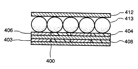
FIGS. 4A and 4I3 illustrate a cpmplete printed
display system with a corlt~ir.uous nonl. ine,.~r_-element
backplane. The device in; lL~des a sub;str;-ate
CA 02284057 2002-07-16
74611-63
16
TM
400, which is typically a thin, flexible material such as KAPTON film. The
row electrodes 402 have preferably been deposited on substrate 400 by
means of a printing process. In the illustrated embodirnent, the nonlinear
backpiane 404 is a continuous layer of either particulate varistor material or
particulate diode material. The structure represented at 404 may also be a
layer of particulate silicon, a printed metal contact and then another layer
of
particulate silicon. Alternatively, the structure 404 may comprise layers of
P- and N-doped particulate semiconductor inks, printed in an ascending
pattern such as PNPNPNNPNPNP. An arbitrarily large number of layers rnay
be printed, the optimal number depending primarily upon the desired
breakdown voltage.
An optional second set of printed row electrodes 406 (shown only in
FIG. 4A), aligned with the first set 402, provide a contact to the other side
of the nonlinear material 404. An insulator material, such as Acheson
1 5 ML25208, is print-deposited in the lanes 408 defining the space between
electrodes 402, so that a smooth surface is formed. An electrooptic display
410, such as a layer of electrophoretic display microcapsules, is print-
deposited onto electrodes 406 or, if these are omitted.. onto nonlinear
backplane 404. A set of transparent column electrodes 412 is print-
deposited onto display 410 in a pattern orthogonal to row electrodes 402
(and, if included, 406). An insulator material is print-deposited in lanes 414
between electrodes 412. Active picture elements are defined in the regions
of display 410 where these orthogonal sets of electrodes overlap. Thus, a
display with M row electrodes and N column electrodes has M x N picture
elements.
The material of nonlinear backplane 404 can be continuous or
deposited as a discrete array, e.g., in a matrix pattern with nonlinear
material
printed only in the areas of active picture elements (i.e., where row and
CA 02284057 2002-07-16
74611-63
17
column electrodes overlap). Such an arrangement is depicted in FIGS. 4C
and 4D. A substrate 430, typically composed of a thin, flexible material
TM
such as KAPTON film, underlies a set of row electrodes 432 which
preferably have been deposited on the substrate by means of a printing
process. The nonlinear backplane 434, which may comprise printed back-to-
back diodes or printed varistor material, is deposited in a pattern
corresponding to the active picture efements~--that is, where the row and
column electrodes cross. An insulator material 435 is deposited so as to
surround elements 434 and thereby create a uniform planar surface. Once
again, the structure represented at 434 may also be a layer of particulate
silicon, a printed metal contact and then another layer of particulate
silicon.
Alternatively, the structure 434 may comprise layers of P- and N-doped
particulate semiconductor inks, printed in an ascending pattern such as
PNPNPNNPNPNP. An arbitrarily large number of layers may be printed, the
1 5 optimal number depending primarily upon the desired breakdown voltage.
An optional second set of printed row electrodes 436, aligned with
the first set 432, provide a contact to the other side of the nonlinear
material
434. An insulator material, such as Acheson ML25208, is print-deposited in
the lanes 438 defining the space between electrodes 432. An electrooptic
display 440 is print-deposited onto electrodes 436 or, if these are omitted,
onto nonlinear backplane 434. A set of transparent column electrodes 444
is print-deposited onto display 440 in a pattern orthogonal to row electrodes
432 (and, if included, 436). Active picture elements are defined in the
regions of display 440 where these orthogonal sets of electrodes overlap. An
insulator material is print-deposited in lanes 4446 between electrodes 444.
FIG. 5 depicts a screen-printed display 500 in the form of the letter
'M'. The display 500 is a layered structure, the layers corresponding to
those shown sectionally in FIGS. 4A and 48. The result is a nonemissive,
CA 02284057 1999-09-17
WO 98/41898 PCT/US98/04842
18
screen-printed, microencapsulated electrophoretic display, printed on an
arbitrary substrate in an arbitrary shape.
FIGS. 6A and 6B show a scheme for addressing a display where the
top electrode is "floating," i.e., not electrically connected. This greatly
simplifies the layout, although at the cost of increasing the required supply
voltage; the depicted arrangement also envisions pixelwise addressing. With
reference to FIG. 6A, a series of display elements 602 each overlie an
associated electrode 604, all of which are carried as a pixel array on a
substrate 606. A single floating plate electrode 608 overlies the displays
602. Alternatively, as shown in FIG. 6B, the display may be a continuous
element substantially coextensive with substrate 606; discrete regions of
such a display, which lie above and are separately addressed by each of the
electrodes 604, act as individual pixels.
Electrodes 604 are spaced apart from one another by a distance s,
and with the components in place, are separated from electrode 608 by a
distance r. So long as r < < s, placing two adjacent electrodes 604 at V~
and V2 induces a potential of (V~ +V2)/2 at electrode 608; accordingly, as a
result of the arrangement, the field across display medium 602 will be half
that which would be achieved were Vi and V2 applied directly. More
specifically, suppose, as shown in FIG. 6B, that a first electrode 6041 is
grounded and a second electrode 6042 connected to a battery 620 of
voltage V. In this case the induced voltage in electrode 608 is V/2, but the
electric field F traverses the display 605 in opposite directions above
electrodes 604, 6042. As a result, assuming that the voltage V/2 is
sufficient to cause switching of display 625 within an acceptable switching
time, the regions of display 625 above the two electrodes will be driven into
opposite states.
CA 02284057 1999-09-17
WO 98/41898 PCT/US98/04842
19
This arrangement cannot sustain a condition where every display
element (or region) is in the same state. To provide for this possibility, a
separate electrode fi50 (and, if the display is organized discretely, a
corresponding display element 652) are located outside the visual area of the
display-that is, the area of the display visible to the viewer. In this way,
electrode 650 may Ibe biased oppositely with respect to all other pixels in
the
device without visual effect.
Refer now to FIGS. 7A and 7B, which illustrate remote powering of
displays. With particular reference to FIG. 7A, a capacitive arrangement
comprises a logic/contral unit 700 and a pair of transmitting electrodes 710
connected thereto. A display unit or "tag" 720, which may have a nonlinear
backplane, is connected to a complementary pair of receiving electrodes
730. Upon application of an AC signal to transmitting electrodes 710, an
AC field is induced in receiving electrodes 720 as they physically approach
the transmitting elecarodes. The current produced by this field can be used
to directly power display unit 720 (e.g., after being passed through a
rectifier), or it can instead be filtered or otherwise processed by on-board
logic in display 720.. For example, the AC signal can convey information to
such display logic to determine the appearance of the display. For example,
one or more notch filters can be employed so that upon detection of a first
AC frequency, the clisplay 720 is placed into a certain state, and upon
detection of a second AC frequency, is changed into a different state. With
the addition of nonlinear elements, more sophistical signal processing can be
effected while retaining the simple circuit design of FIG. 7A. All electronic
elements associatecl with logic unit 700 and display unit 720 may be
generated by a printing process.
FIG. 7B shovws an inductive approach to remote powering and
signalling. The illustrated inductive arrangement includes a logic/control
unit
CA 02284057 1999-09-17
WO 98/41898 PCTNS98/04842
740 and one or more transmitting coils 750. A display unit or tag 770,
which may have a nonlinear backplane, is connected to a complementary
pair of receiving coils 760. Upon application of an AC signal to transmitting
coils 750, the resulting magnetic field induces an AC current in receiving
5 coils 760. The induced current can be used to directly power display unit
770 or convey information in the manner described above. Once again, the
arrangment may include notch filters or additional nonlinear elements for
more sophistical signal processing. All electronic elements associated with
logic unit 740 and display unit 770 may be generated by a printing process.
10 Refer now to FIGS. 8A and 8B, which illustrate application of the
invention to create a voltage scale (which may serve, for example, as a
battery indicator). The display system 800 includes a series of individual
particle-based (preferably electrophoretic) display devices 810 mounted on a
substrate 820. Each display device 810 includes a rear electrode, a
15 nonlinear device, a display element (which may be discrete or shared among
all devices 810), and a transparent electrode; these components are
preferably printed in a stack structure in the manner illustrated in FIG. 6A.
As shown in FIG. 8B, each display can be represented as a nonlinear
device 830 ... 830 and a capacitor 8401 ... 840. The nonlinear devices
20 830 have progressively higher breakdown voltages. Accordingly, the
number of such displays "turned on" (or "turned off") at any time reflects
the voltage (e.g., from a battery 850) across the displays. In operation, all
of the displays 810 are initially in the same state. Each of the displays 810
changes state only when the potential exceeds the breakdown voltage of the
associated nonlinear device. To reset the device, the user activates a switch
(not shown) which reverses the connection of battery 850 and causes it to
generate a potential exceeding the breakdown voltages of all nonlinear
devices 830.
CA 02284057 1999-09-17
WO 98141898 PCT/US98/04842
21
It will therefore be seen that the foregoing represents a versatile and
convenient approach to the design and manufacture of particle-_based display
systems. The terms and expressions employed herein are used as terms of
description and not of limitation, and there is no intention, in the use of
such
terms and expressions, of excluding any equivalents of the features shown
and described or portions thereof, but it is recognized that various
modifications are possible within the scope of the invention claimed.