Note: Descriptions are shown in the official language in which they were submitted.
CA 02284065 1999-09-17
WO 98/42066 PCT/US98/05425
HIGH POWER 1:NVERTER POLE EMPLOYING SERIES CONNECTED
DEVICES CONFIGURED FOR REDUCED STRAY LOOP INDUCTANCE
BACK 'ROUND OF THE INVENTION
Field of the Invention
This invention relates generally to power electronic compensators for electric
utility transmission anal distribution systems. More particularly, this
invention relates
to very high power voltage sourced inverter poles employing a number of series
connected semi-conductor switching devices.
Background Informat{gn
New applications of pawer electronic equipment to electric utility
transmission
and distribution systems will greatly improve the reliability and utilization
of such
systems. Some of these applications, such as the "Static VAR Compensator"
(STATCUN), employ voltage sourced inverters to control reactive power. Other
applications use voltage sourced inverters which handle both real and rezctive
power
to improve the control characteristics of individual transmission lines within
a network.
For distribution systems, large but somewhat smaller inverters used for
similar
purposes can also provide harmonic compensation for nonlinear loads.
i5 To achieve the required power ratings, these inverters employ series
connected
switching devices to make up "high voltage valves." For distribution systems,
pulse
width modulated invE;rters rated from 1 to IOMW typically operate from do
voltages
of 2 to 6kV and employ fast switching devices such as insulated gate bipolar
transistors
{GBTs). For very huge transmission type applications, "Gate Turn-Off
Thyristors"
(GTOs) are used to make up high voltage valves capable of switching currents
of 2- .
4kA and blocking voltages of 10-20kV.
CA 02284065 1999-09-17
WO 98/42066 PCT/ITS98/05425
-2-
Typically, in these applications, the inverter poles consist of two valves
connected in series across a de voltage source, with the ac output taken from
the mid
point. Complete inverters employ a number of inverter poles, usually in sets
of three.
The valves in these inverter poles switch alternately to produce square wave
or pulse
width modulated ac outputs. The phase shifted outputs of the multiple sets of
poles are
combined by special interface magnetics to produce a stepped approximation of
a sine
wave.
At each switching event, load current is commutated alternately from the valve
connected to one do bus to the other. When a valve turns off, its current is
suddenly
interrupted: however, because of stray inductance, this current cannot
immediately be
picked up by the oncoming valve and it will initially start to charge the
capacitance
which appears across the outgoing valve. If this capacitance is small and
there is no
damping, the voltage developed across the outgoing valve can significantly
exceed the
dc-source before the commutation is completed. To accommodate this overshoot,
the
voltage rating of the valve must be significantly greater than the dc-source
voltage to
which it is normally exposed. Depending on the type of switching devices
employed.
the overshoot voltage may be limited by different methods such as snubber
capacitors
and voltage clamping devices.
For high voltage applications, each of the valves is made up of a number of
series connected switching devices. The number of devices required depends
upon the
withstand voltage of the device and the magnitude of the overshoot voltage.
The switching devices in each of the valves is shunted by an anti-parallel
diode
to accommodate for power factors other than one which result in a difference
in
polarity between the ac current and voltage during a portion of each cycle of
the
output. This can result in a momentary short circuit across the ac bus when
the other
CA 02284065 1999-09-17
WO 98/42066 PCT/US98/05425
-3-
valve turns on, until the anti-parallel diodes stop conducting. It is known to
insert di; dt
reactors in series on the do side of the inverter to limit this current. These
inverters
are shunted by diodes and resistors to dissipate the energy stored during
switching.
Despite efforts made to date to minimize the overshoot voltage imposed on the
series connected devices of high power voltage sourced inverter poles, there
is need
for improvement.
There is also a need for reducing the overshoot voltage in such inverter poles
without incurring substantial losses.
SUMMARY OF THE INVENTION
These need and others are satisfied by the invention which is directed to
limiting
the total unclamped stray loop inductance of a high power voltage sourced
inverter pole
in order to minimize the overshoot voltage during commutation. This is
achieved by
mounting positive and negative switching valves, each made up of a set of
series
connected switching units and connected between closely spaced, positive and
negative
IS do terminals, respetaively, ~uld a common ac terminal, so as to form a loop
with
minimum loop area. In one embodiment of the invention, the positive and
negative
switching poles are: connected back-to-back and extend linearly between the do
terminals and the ac terminals. In another embodiment, sections of the
electrical path
formed by each of the positive and negative poles are folded back on each
other
between the do terminals and the ac terminal, again forming a loop with
minimum loop
area. To further reduce the stray loop inductance of the switching poles, the
individual
switching units of mch of the switching valves are connected by broad, flat
conductors
. which emulate a strip line. The width of these flat conductors is at least
equal to the
spacing between conductors on facing sides of the loop. Preferably, this
aspect ratio
of width to spacing is at least about 4 to 5:1.
CA 02284065 1999-09-17
WO 98/42066 PCT/IJS98/05425
As another aspect of the invention, an elongated insulative member is provided
between the positive and negative switching valves to provide greater stand
off voltage
capability and, therefore, permit their being positioned close together to
minimize the
loop area. This elongated insulated member also serves as a mount for the
positive and
negative switching valves. In a particularly advantageous arrangement, this
elongated
electrically insulative member is contigured as an I-beam which provides
structural
rigidity for the switching pole and, with the switching poles placed adjacent
opposite
sides of the beam web, the beam flanges provide increased creep distance
between the
positive and negative electrical paths.
IO An important aspect of the invention is that the switching units are
modular s::d.
therefore, can be separately tested and replaced as necessary. These modular
switch
units each comprise a switch, an anti-parallel diode shunting the switch, and
a pair of
spaced apart, flat conductors between which the switch and the anti-parallel
diode are
sandwiched. As in the case of the connecting conductors, the aspect ratio or
width of
these flat conductors to the spacing between them is at least equal to about
l: l and
preferably is at least 4 to 5:1. These flat conductors of the switch units
serve as
electrical conductors and heat sinks for the switch and the anti-parallel
diode.
Preferably, they have passages for circulating coolant to cool the switch and
anti-
parallel diode. The flat conductors of the modular switch units are connected
to and
extend transversely outward from the broad, flat connecting conductors of the
switching
valves which connect the modular switching units in series. The modular
switching
units further include snubber capacitors and resistors which are also
connected by flat
conductors to reduce stray loop inductance. The flat connecting conductors
are,
preferably C-channel sections having channel flanges secured to the I-beam
flanges and
CA 02284065 1999-09-17
WO 98/42066 PCT/US98/05425
-5-
having channel webs adjacent the beam web. In this conriguration, the metal C-
channel connecting ~~onductors strengthen the fiber glass I-beam.
The switching poles which are supported by the elongated insulative member
such as an I-beam or back-to-back C-channels can be stacked one on top of each
other,
for instance to provide a six-pulse inverter bridge producing a three-phase ac
output.
CA 02284065 1999-09-17
WO 98/42066 PCT/US98/05425
-6-
BRIEF DESCRIPTION OF THE DRAWINGS
A full understanding of the invention can be gained from the following
description of the preferred embodiments when read in conjunction with the
accompanying drawings in which:
Figure 1 is a simplified schematic diagram of a conventional prior art high
voltage inverter pole.
Figure 2 is a simplified schematic diagram of a high voltage inverter
switching
pole in accordance with a first embodiment of the invention.
Figure 3 is a simplified schematic diagram of a high voltage inverter
switching
pole in accordance with a second embodiment of the invention.
Figure 4 is a more detailed schematic diagram of the embodiment of the
switching pole shown in Figure 2.
Figure 5 is an isometric view of a switching pole in accordance with the
embodiment of the invention shown in Figures 2 and 4 with some parts removed
for
clarity.
Figure 6 is an isometric view of a modular switching unit in accordance with
the invention.
Figure 7 is an isometric view of one flat conductor which forms a pan of the
modular switch unit of Figure 6.
Figure 8 is an isometric view of the other flat conductor which forms part of
the modular switch unit of Figure 6.
Figure 9 is a cross section through a switching pole in accordance with the
embodiment of Figure 5 incorporating modular switching units of Figures 6-8.
Figure 10 is an isometric view of three stacked switching poles in accordance
with the invention forming a six-pulse inverter bridge.
CA 02284065 1999-09-17
WO 98/42066 PCT/US98/05425
_7_
DESCRIPTION OF THE PREFERRED EMBODIMENT
Figure 1 illustrates schematically a conventional high voltage inverter pole
using
series connected switches. This inverter switching pole 1 has a positive
switching
valve 3 and a negative switching valve 5, each made up of a number of series
connected switches 7a-7j shunted by an anti-parallel diode 9a-9j. As
previously
discussed, the switches 7a-7j can be, for example, IGBTs for distribution
systems and
GTOs for transmission line applications. The switching pole 1 is fed by a do
source
11 through a positive do terminal 13 and a negative do terminal 15. The
positive valve
3 and negative valve: 5 are connected in series between the positive do
terminal 13 and
negative do terminal. 15. The ac output is provided through an ac output
terminal 17
connected at the mid point between the positive and negative valves 3 and 5.
Typically, such conventional inverter switching poles are laid out without
regard to
stray inductance, for instance, such as in the arrangement shown in Figure 1.
That is,
the positive and negative valves 3 and 5 are linearly connected between the
spaced
apart positive and negative do terminals 13 and 15. We have recognized that
this
configuration results in high stray loop inductance which contributes to high
overshoot
voltage during swi~;ching of the switches 7a-7j. While snubber circuits and
other
elextrical limiter components have been provided in attempts to control the
overshoot
voltage, we have treen able to further reduce the overshoot voltage. Among the
benefits of reduction in the overshoot voltage is the reduction in the number
of switches
. 7a-7j required in a particular application.
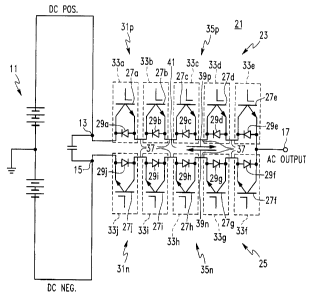
Figure 2 illustrates schematically a first embodiment of the invention. This
switching pole 21 also includes a positive switching valve 23 and a negative
switching
valve 25, each hauling a number of switches 27a-27j each shunted by an anti-
parallel
diode 29a-29j. Switches 27a-27e and their anti-parallel diodes 29a-29e form a
first set
CA 02284065 1999-09-17
WO 98/42066 PCT/US98/05425
_g_
31 p of switching units 33a-33e. These switching units 33a-33e are connected
in series
by a first set 35p of connecting conductors 37 to form a positive electrical
path 39p.
Similarly, the negative valve ~5 is made up of a second set 31 n of switch
units 33 f-33j
which are connected in series by a second set 35n of connecting conductors 37
to form
a negative electrical path 39n. In the inverter pole of Figure '_', the
positive terminal
13 and negative terminal 15 of the dc-source 11 are spaced close together and
apart
from the ac terminal 17. The positive switching valve 23 is connected linearly
between
the positive do terminal 13 and the ac terminal 17, while the negative
switching valve
?5 is connected between the negative do terminal 15 and the ac terminal 17.
Thus, the
positive switching valve and negative switching valve 25 are connected back-to-
back
with the positive electrical path 39p and the negative electrical path 39n,
forming a
loop 41 having a minimum loop area. A limiter 43 in the form of a do voltage
clamping capacitor 45 is connected across the closely spaced de terminals 13
and 15.
Other conventional limiters can be utilized, as will be discussed below,
Figure 3 illustrates another embodiment of a high power switching pole ~ 1'
for
a voltage sourced inverter. In this arrangement, the positive electrical path
39p' of the
positive switching valve 23' has a first section 39p, containing the switching
units 33,
and a second section 39p2 made up only of an elongated connecting conductor
37' with
the two sections folded back on each other between the positive do terminal 13
and the
ac terminal 17. Likewise, the negative electrical path 39n' is made up of two
sections,
39n, containing the switching units 33 and 39nz made up of only an elongated
connecting conductor 37. These electrical paths also form a loop 41' having
minimum
loop area thereby reducing the stray loop inductance of the switching pole
21'. In an
alternative arrangement, not shown, the switching units 33 in each of the
positive
switching valve 23' and negative switching valve 25' can be distributed in
both sections
CA 02284065 1999-09-17
WO 98/42066 PCT/US98/05425
-9-
of the respective electrical paths. Again, the switching pole 21' is fed by
the dc-source
11 through the do terminals 13 and 15 which are closely spaced and across
which a
clamping capacitor 4:5 is connected.
Figure 4 is a more detailed schematic illustration of the switching pole '_' 1
of
Figure 2. The switching units 33 which make up the positive valve ~3 and
negative
valve 25, modular units which are easily inserted and removed through
connections.
to be described, to the connecting conductors 37. Each of the modular
switching units
33 includes the switch 27 such as, for example, GTO or iGBT, shunted by an
anti-
parallel diode 29.
In order to limit the rise of voltage at turn-off of the switches '_'7, the
limner
devices 43 include snubber capacitors 47 connected across the switches 27, so
that
when the switch turns off the current immediately begins to charge the
capacitor .~7.
These snubbing capacitors 47 then discharge through a snubber discharge
resistor .~9
and a resistor 51 connected across the switch 27. This resistor 51 also sewes
to
equalize do voltage ticross the series connected switches 27. The limiter
devices -~3
also include a snubbe.r diode _'~3 which prevents reverse flow of current when
the switch
27 again turns on. A secondary snubber capacitor 55 prevents ringing when the
snubber diode 53 suddenly blocks. A damping resistor 57 is connected in series
with
the secondary snubb~er capacitor 55.
As mentioned previously, means must be provided to limit the rate of change
of current at turn on of the switches 27. Thus, the limiter devices 43 include
a pair
of air core reactors 59p and 59n connected in series with the positive
switching valve
. 23 and negative switching valve 25, respectively. Because the current
tlowing in the
dildt reactors 59p and 59n cannot immediately change when a switch 27 blocks,
it will
continue to flow untiil it reaches zero. Normally, this would not occur until
the voltage
CA 02284065 1999-09-17
WO 98/42066 PCT/US98/05425
- 10-
on the snubber capacitor 47 reaches a peak well above (typically as much as
twice) the
voltage of the dc-source 11, and the switches 27 would have to be rated to
block this
voltage.
In order to limit the voltage overshoot, diodes 61 p and 61 n can be connected
to the larger clamping capacitor 45 which will charge relatively slowly to a
voltage
slightly above the dc-source voltage. The excess voltage on the capacitor .t5
is then
partially returned to the dc-source 11 through two damping resistors 63p and
63n.
With this arrangement, the overshoot voltage is effectively limited, and some
of the
trapped energy is recovered. However, even with this known clamping circuit,
there
will be some voltage overshoot due to the self-inductance of the loop formed
by the
conductors connecting the switches to the clamping capacitor and the
inductance of the
clamping capacitor itself.
The physical arrangement of a switching pole 21 in accordance with the first
embodiment of the invention is illustrated, in simplified form in Figure 5,
and in the
cross section shown in Figure 9. The positive switching valve 23 and negative
switching valve 25 are mounted back-to-back by a mounting arrangement which
includes an elongated electrically insulative member in the form of a fiber
glass I-beam
65. This I-beam 65 is supported with its web 65w oriented vertically and its
flanges
65f extending horizontally. The switching units 33 of the positive switching
valve ?3
and negative switching valve 25 are modular units which include a pair of
spaced apart.
flat conductors 67 and 69.. The additional details of the modular switching
units _ 3 are
not shown in Figure 5 for clarity, but are described in detail below. The
modular units
33 of the positive switching valve 23 and negative switching valve 25 are
connected
in series on opposite sides of the beam web 65w by the broad, flat connecting
conductors 37. Preferably, these broad, flat connecting conductors are in the
form of
CA 02284065 1999-09-17
WO 98/42066 PCT/US98/05425
C-channels having a ~:hannel web 37w and flanges 37f. These connecting
conductor
C-channels are mounted to the I-beam 65 with the channel webs 3 7w adjacent
the beam
web 65w and with the'-channel flanges 37f bolted to the beam flanges 65f by
fasteners
71. This arrangemen~permits the positive and negative switching valves ?3 and
'_'S to
be placed close together to reduce the stray loop inductance while at the same
time
providing electrical i~~olation with the flanges 65f of the I-beam providing
increased
creep distance betweF;n the opposite polarity switching valves. Furthermore,
the C-
channel connecting conductors provide stiffening for the tiber glass I-beam
65. The
ratio of the width of the webs 37w of the C-channels 37 to the spacing being
webs on
opposite sides of the web 65w of the I-beam produces an aspect ratio of at
least 1:1
and preferably 4 to 5:1 for the tlat connecting conductors.
The positive and negative do conductors 13 and 15 extend along opposite sides
of -he I-beam web 6_'i at one end of the I-beam, while the connecting plates
37 at the
opposite ends of the :.witching valves 23 and ~5 are connected to a common ac
output
conductor 73 at the other end of the I-beam. The di/dt reactors 59p and 59n
are
connected between the positive and negative do terminal conductors 13 and 15
and the
first connecting conductor of the respective switching valve by broad, tZat
conductors
75p and 75n. Clamping capacitor 45 is mounted on top of the I-beam 65 with the
damping resistors 63 mounted between the capacitor and the do terminal
conductors by
flat L conductors 77. The diode 61 are sandwiched between broad, flat
conductors 79
between the clamping capacitor 45 and the switching valves 23 and 25.
'The details of the maduiar switching units are shown in Figures 7-9. The
broad, flat conductors 67 and 69 of the modular units 33 have flanges 67f and
69f
which bolt to the channel webs 37c of the connecting conductors so that the
modular
units 33 extend transversely outward from the I-beam 65. The switch 27, such
as a
CA 02284065 1999-09-17
WO 98142066 PCT/US98/05425
- 12-
GTO or IGBT, and the anti-parallel diode 29 of the switch unit are sandwiched
Getween the flat conductors 67 and 69. This is effected by clamps 81 formed by
clamping bars 83 drawn together by clamping bolts 85 which extend through
apertures
or slots in the flat conductors 67 and 69. Clamping plates 87 under the
clamping bars
83 distribute the clamping force for better electrical and heat transfer
contact between
the electrical components and the flat conductors 67 and 69. A shunt plate 89
electrically connects upper and lower sections 69u and 691 of the conductor
69. In
addition to providing electrical connections and mechanical support for the
switches =''
and the anti-parallel diode 29, the flat conductors 67 and 69 serve as heat
sinks to
LO dissipate the considerable amount of heat generated by the high power
handled by the
switching units. Dissipation of heat is enhanced by circulating cooling water
through
passages 91 within the flat conductors 67 and 69. The cooling water is
supplied
through mains 93 mounted underneath the I-beam 65 (see Figure 9). Hoses 95
connected to the mains, and connecting hose 97 connected between the
conductors 67
and 69, provide a path for circulating coolant through the passages 91. The
flat
conductor 69 is elongated and has pipes 99 for circulating the cooling water
through
the remote end of the conductor. As in the case of the connecting conductors
37, the
spaced apart, flat conductors 67 and 69 have an aspect ratio of width to
spacing of at
least 1:1, and preferably at least 4 to 5:1.
The flat conductors 67 and 69 also serve as mounts and heat sinks for the
remaining components of the switching units 33. The various resistors of the
switching
unit are mounted in finned housings with a flat surface for engaging one of
the flat
conductors/heat sinks 67 or 69. The do voltage equalizing resistor 51 is
formed by two
such resistors S la and S lb bolted to the conductors 67 and 69, respectively,
and
connected by a lead S lc. The other ends of the resistors are connected
electrically to
CA 02284065 1999-09-17
WO 98/42066 PCT/US98/05425
- l3-
the flat conductors 67 and 69 and, therefore, across the switch ~7, by
additional leads
Sld. The snubber discharge resistor 49 is formed by six resistors mounted
three on
each side of the end of the flat conductor b9 and connected in parallel by
flat
conductors lOla, electrically connected to flat conductor 69, and flat
conductor lOlb
spaced from the end of the flat conductor 69. Secondary snubber resistor ~7 is
mounted on the side of the flat conductor 69. The snubber capacitor .t7 is
supported
at one end by a flat conductor 103 bent to form a supporting flange i03f. The
other
end of flat conductor 103 is connected to the snubber diode 53 (see Figure 9)
which
is sandwiched between insulating plates (not shown) clamped between the flat
conductors 67 and 69~ by a clamp 105. The secondary snubber capacitor 5~ is
also
supported by the tla~~ge 103f which forms a common electrical node through
flat
conductor 106. The snubber discharge resistors 49 are connected to this common
node
by the t3at conductor 107. The other end of the snubber capacitor 47 is
supported by
a flat conductor 109 ~~uspende.d from the other flat conductor/heat sink 67.
The other
end of the secondary snubber capacitor 55 is connected to the damping resistor
57 by
a flat conductor 111. These connections implement the module circuits shown in
Figure 4. The flat conductors used throughout help to reduce the stray
inductance and,
therefore, the overshoot voltage during switching.
Returning to Figure 5, a pole electronics box 113 generates high frequency
(e.g.
~0 kHz) power for operating the pole switch units 33. This power is delivered
over
power leads 115 extending along the top of the I-beam 65 to individual control
boxes
117 for each of the modular switching units. These control boxes 117, which
are also
mounted on top of the I-beam by the fasteners 71, draw power from the leads
115
through current transformers 118 which provides good electrical isolation
between
units. The control boxes 117 generate the signals on leads 119 which control
the states
CA 02284065 1999-09-17
WO 98/42066 PCT/US98/05425
- 14-
of the switches 27 of the associated modular units 33 in response to tiring
signals
generated by a control system (not shown) and transmitted to the control boxes
l 1 %.
Figure 10 shows how three poles 2, to 2, can be stacked to form a six-pulse
inverter bridge. The I-beams 65, to 65, of the respective poles are supported
at each
end by a transverse I-beam section 121, to 121,. Each end of each of the
transverse
I-beam sections 121 is supported by an insulative column 123. Multiple six
pulse
inverter bridges 125, such as shown in Figure 10, can be combined to produce a
harmonic neutralized stepped approximation of a sinewave, which can be used.
for
instance, in providing compensation in an electric power transmission or
distribution
system.
While specific embodiments of the invention have bean described in detail, it
will be appreciated by those skilled in the art that various modifications and
alternatives
to those details could be developed in light of the overall teachings of the
disclosure.
Accordingly, the particular arrangements disclosed are meant to be
illustrative only and
not limiting as to the scope of invention which is to be given the full
breadth of the
claims appended and any and ali equivalents thereof.