Note: Descriptions are shown in the official language in which they were submitted.
CA 02284072 1999-09-17
WO 98/44769 PCT/GB97/03558
- 1 -
I~UI~DED SOCI~~TS FOR ELECTRONIC C~ONENT ATTACBMENT
The present invention relates generally to the mounting
of electronic components. More particularly, the present
invention relaters to mounting electronic components to
three-dimensiona:L-surface substrates using moulded sockets.
The attachmE~nt of electronic components to circuit
board substrates is typically achieved by soldering.
Various soldering techniques are used in the electronics
to industry, including th~a conventional practices of reflow
soldering, wave ~~older:ing, and vapour-phase soldering. Each
of these processes requires the use of metal alloy solders
that process at relatively high temperatures. Furthermore,
each of these processes has been developed for use with
i5 planar circuit boards.
Recently, interest: has grown in the use of non-planar
(i.e., "three-dimensional" or "curviplanar") circuit
substrates as a more flexible design alternative to
conventional planar circuit boards. For example, as
2o illustrated in FIG. 1A, circuits and components which in the
past were placed on rigid, planar circuit boards 60 with the
boards then being attached by fasteners 64 to a moulded
plastic housing 62, are now being placed directly on an
interior or exterior surface of the housing itself, as shown
25 in FIG. 1B. In this type of arrangement, the surface of the
moulded housing 62 is typically metallised and the
electronic components and circuitry are soldered thereto,
the housing thus replacing the planar circuit board and
serving as the substrate for the components and circuitry.
3o This arrangement offers the advantage of integrating the
electronics together with the structural housings or other
adjacent moulded structures, thus reducing the number of
processing steps, eliminating unnecessary fasteners and
other hardware 64, and reducing overall product costs.
3s However, this type of integrated structure suffers from
its inability to :be processed using conventional soldering
techniques, for at least two reasons. First,~the non-planar
CA 02284072 1999-09-17
WO 98/44769 PCT/GB97/03558
- 2 -
surfaces of such integrated structures cause the structures
to be incompatible with conventional soldering equipment,
such as reflow ovens and the like, which can only process
planar substrates. Second, the plastic resins used to make
such integrated structures often cannot withstand the
thermal excursions and/or chemical attack of conventional
solder processing.
It would be desirable, therefore, to provide a way of
integrating electronic circuitry with three-dimensional
to moulded substrates in such a way that would eliminate the
need for soldering altogether.
The present invention provides an electrical circuit
assembly which requires no solder processing, comprising an
electronic component having terminations arranged on at
least one of its surfaces, and a moulded curviplanar
substrate having circuit traces thereon and a cavity formed
therein, wherein the cavity substantially conforms in shape
with the electronic component. Proximate the cavity is a
plurality of electrical contacts, arranged in matched
2o relation with the respective terminations of the electronic
component, with at least one of the electrical contacts
being connected to at least one of the circuit traces on the
substrate. The cavity and electrical contacts are
dimensioned such that an interference fit is provided
between the component's terminations and the electrical
contacts, such that the component is held within the cavity
when the component is placed therein. The component is
disposed in the cavity such that its terminations are in
physical and electrical connection with their respective
3o electrical contacts. The invention may also include such
additional features as an adhesive placed between a bottom
surface of the electronic component and a respective surface
of the cavity, and an overmolding of electrically insulative
material sealably covering each electronic component and a
portion of the substrate peripherally adjacent each
electronic component.
CA 02284072 1999-09-17
WO 98/44769 PCT/GB97/03558
- 3 -
It is an advantage of the present invention that
electronic circuits and components may be directly
integrated with structural housings or other curviplanar
moulded substrates, thus reducing processing steps, the
number of parts .required, and overall product costs.
Another advantage of the present invention is that such
integration of electronic circuits and components with
curviplanar moulded substrates may be accomplished without
the use of solder processing.
io Yet another advantage of the present invention is the
ability to use low-temperature-melting plastic as a
substrate materi<~l for such electronic circuits and
components.
The invention wil.1 now be described, by way of example,
with reference to the accompanying drawings, in which:
FIGS. lA an<i 1B a:re perspective views of moulded
structures couplE~d with electronic components and
circuitry according to the prior art;
2o FIGS. 2A-2C are e:Levational cross-section views of a
first embodiment of the present invention, showing,
respectively, electronic components before, during, and
after insertion into their respective cavities;
FIGS. 3A-3H are perspective views of various electronic
components which may bE~ used in a first embodiment of the
present invention, along with their respective cavities;
FIGS. 4A anc~ 48 ar_e top plan views of cavities for
bottom-terminated electronic components, shown before and
after electrical contact deposition, as viewed along section
lines 1-1 and 2-2, of FIGS. 3D and 3E, respectively;
FIGS. 5A-5D are elevational cross-section views of
additional configurations according to a first embodiment of
the present invention showing nib-leaded electronic
components beforE~ insertion into their respective cavities;
FIG. 5E is an enlarged, partial view of FIG. 5A,
showing a lip and nibbE:d lead after insertion of the
component into it.s respective cavity;
CA 02284072 1999-09-17
WO 98/44769 PCT/GB97/03558
- 4 -
FIGS. 6A-6D are elevational cross-section views of a
second embodiment of the present invention, showing, leaded
electronic components before insertion of their leads into
their respective receptacles;
FIGS. 7A-7D are perspective views of receptacle
openings according to a second embodiment of the present
invention:
FIG. 8 is an elevational, cross-sectional end view of a
trough-like receptacle opening, as viewed along section line
l0 8-8 of FIG. 7B;
FIGS. 9A-9D are elevational cross-section views of
additional configurations according to a second embodiment
of the present invention.;
FIG. 10 is a perspective view of an additional
configuration according to a first embodiment of the present
invention, showing a cavity and contacts incorporating a
through-hole conductive path between the first and second
substrate surfaces; and
FIG. 11 is an elevational cross-section view taken
2o along section line 3-3 of FIG. 10.
Referring now to the drawings, FIGS. 2A-2C show a first
embodiment of the present invention wherein an electronic
component 10 is electrically connected to circuit traces 30
arranged on a first surface 22 of a generally curviplanar
moulded plastic substrate 20, without the use of solder.
The substrate 20 may also have a second surface 23 generally
conforming in shape with that of the first surface 22. The
first surface 22 and second surface 23 may be exterior and
3o interior surfaces of the substrate 20, respectively, or vice
versa. In this embodiment, the electronic component 10 has
a body 12 with terminations 14 arranged on at least one
surface thereof. A cavity 24 is formed on the first surface
22 of substrate 20, but does not extend through to the
substrate's second surface 23 (i.e., the cavity 24 is not a
through-hole). The shape of the cavity 24 substantially
conforms with that of the component 10 to be placed therein.
CA 02284072 1999-09-17
WO 98/44769 PCT/GB97/03558
- 5 -
Examples of such components 10 and their respective cavities
24 are shown in FIGS. 3A-3H.
Proximate the cavity 24 a plurality of electrical
contacts 40 are arranged in matched relation with the
terminations 14 of the component 10. At least one of these
contacts 40 is connected to at least one circuit trace 30 on
the substrate 20. These contacts 40 may consist of
metallisations, foils, thin conductive films, pins, plates,
etc. and may be formed by such processes as chemical
io plating, vacuum metal vapour deposition, flex circuit in-
moulding, insert moulding, lamination, embossing, adhesion,
and the like. For example, the electrical contacts 40 may
be tin metallisations deposited directly onto the substrate
20 (and in contact with the appropriate copper circuit
traces 30) by el~~ctrodeposition. The contacts 40 may also
be constructed using multiple layers of metallisations. For
example, a base metallisation of copper may be deposited
onto the substrate 20 when the circuit traces 30 (also
typically copper) are placed thereon. On top of this base
2o metallisation a aecond layer consisting of tin may then be
deposited. Addis=Tonally, intermediate layers of metal-such
as palladium, go:Ld, and the like may be sandwiched between
the base metallisation and the outer metallisation, to
prevent the formation of undesirable intermetallic compounds
therebetween. The contacts 40 are arranged on at least the
inner cavity wal:Ls 25, but may also extend onto some portion
of the substrate surface 22 peripheral to the cavity 24
and/or onto some portion of the cavity floor 27.
The component 10 :is placed into the cavity 24 such that
3o its terminations 14 are brought into physical and electrical
connection with their respective contacts 40. This is
facilitated by dimensioning the respective cavity 24 and
contacts 40 for ~i given component 10 such that an
interference fit is provided between the contacts 40 and the
terminations 14 of the component 10, so as to hold the
component 10 within the cavity 24 after insertion is
completed. This is il:Lustrated in FIG. 2B, wherein the
CA 02284072 1999-09-17
WO 98/44769 PCT/GB97/03558
- 6 -
component terminations 14 are shown to encounter an
interference fit with their respective contacts 40 at some
point during insertion of the component 10 into the cavity
24. The inner cavity walls 25 may also be formed with a
draft to further facilitate both insertion and interference.
The tolerance on such dimensions as cavity width, cavity
depth, cavity wall draft angle, contact thickness, and
contact draft angle should be controlled such that the
interference fit will allow the component 10 to be pressed
1o into the cavity 24 to the desired depth while also holding
the component 10 therein, as illustrated in FIG. 2C. This
may be further facilitated by forming the contacts 40 from a
substantially malleable metal alloy, and/or by placing an
adhesive 15 between a bottom surface 16 of the component 10
and a surface of the cavity 24 proximate the component's
bottom surface 16.
The cavity 24 and contacts 40 may be dimensioned such
that the component 10 is positioned so that the component
top surface 17 is substantially flush with the adjacently
2o surrounding substrate surface 22. Additionally, either with
or without the component top surface 17 being flush with the
substrate surface 22, an overmolding or potting 26 may be
placed over a component 10 and a portion of the substrate
surface 22 peripherally adjacent the component 10, thereby
sealing the component 10 from any harsh environmental
factors which may exist, as well as providing additional
means for holding the component 10 within the cavity 24.
Such an overmolding 26 may be composed of a material which
has a coefficient of thermal expansion substantially
3o equivalent to that of the substrate material, so that
thermal strain therebetween may be minimised. The
overmolding 26 may also cover more than one component 10.
The substrate 20 may also include internal voids 29
formed therein proximate the inner cavity walls 25, as
illustrated in FIGS. 2A-2C. These voids 29 provide
additional resilience to the cavity walls 25, thereby aiding
in insertion and retention of the component 1D within the
CA 02284072 1999-09-17
WO 98/44769 PCT/GB97/03558
_ 7 _
cavity 24. The~;e voids 29 may be formed by gas injection or
other means during the substrate moulding process.
Preferably both t:he terminations 14 and the contacts 40
are composed of a metal or metal alloy which is
substantially inert to oxidation, such as gold, palladium,
or alloys of tin., lead, and/or bismuth. Alternatively, the
terminations 14 and/or contacts 40 may have a multi-layer
construction wherein at least the outermost layer is
composed of a metal substantially inert to oxidation, or an
to inorganic antioxidant coating. However, even if the outer
surfaces of the terminations 14 and/or contacts 40 are not
substantially inert, further urging of the component 10 into
the cavity 24 after interference is encountered will cause a
wiping of the terminat:ions 14 against the contacts 40 to
occur, thereby removing at least some of any oxide layer
that may have formed an the terminations 14 and/or contacts
40.
It should be noted that the component 10 may have its
terminations 14b arranged on its bottom surface 16, as
2o illustrated by components lOb and lOc in FIGS. 3D and 3E.
' For such a device, the contacts 40 are disposed on the inner
cavity walls 25 and extend onto the cavity floor 27
underneath and in matched relation to the bottom
terminations 14b. The cavity 24 is dimensioned and the
contacts 40 arranged such that an interference fit is
provided between the component body 12 and the cavity inner
walls 25, so that the component 10 is held within the cavity
24 when the comp~~nent 10 is positioned therein. FIG. 4A
shows that notches 21 may be formed in the inner cavity
3o walls 25 in order to recess the contacts 40 away from the
component body 12, so that the contacts 40 do not interfere
therewith. As an alternative to the notches 21, the cavity
can be dimensioned so that two opposing inner cavity walls
25 or wall portions provide an interference fit with the
body 12 of the component while two other opposing inner
cavity walls 25 or wall portions are spaced apart from the
component body 1:Z. In this arrangement the cbntacts 40 are
CA 02284072 1999-09-17
WO 98/44769 PCT/GB97/03558
_ g _
disposed on the spaced-apart walls 25 or wall portions and
the cavity floor 27. As a further alternative, instead of
an interference fit being provided between the component
body 12 and the cavity inner walls 25, it is possible to
dimension the cavity walls 25 and contacts 40 such that an
interference fit is provided between the component body 12
and the contacts 40 themselves, as illustrated by component
lOc and contacts 40c in FIGS. 3E and 4B.
A wide variety of components can be utilised with this
1o first embodiment. For example, FIGS. 3A-3H show various
terminated components l0e (such as a leadless ceramic chip
carrier, or LCCC), various bottom-terminated devices
10b/lOc, a plastic leaded chip carrier (PLCC) lOp, an
inverted quad-flat-pack (QFP) device lOq, and an inverted
i5 dual in-line package (DIP) device lOd, along with their
respective cavity and contact configurations.
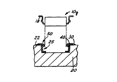
When using J-leaded, gull-winged, or other components
having springlike leads 18 projecting from at least one
edge of the component body 12, wherein the leads 18 are
2o inwardly and resiliently deflectable toward the body 12, the
cavities 24 for such devices may incorporate an additional
feature to aid in holding the component 10 within the cavity
24 after insertion therein. This feature comprises a lip 50
located at an intersection between the inner cavity walls 25
25 and the substrate surface 22, as shown in FIGS. 5A-5E. The
lip 50 extends a predetermined distance into the cavity 24,
and may be formed, for example, by forming a ridge 51 on the
substrate 20 at this location which projects toward the
interior of the cavity 24 (e. g., using cam-actions during
3o the moulding of the substrate 20), followed by deposition of
the contacts 40 over this ridge 51. Alternatively, the
substrate 20 may be formed without such a ridge 52, and the
contacts 40 may consist of metal inserts which have the lip
50 formed thereon, the inserts then being affixed to the
s5 substrate 20 proximate the cavity so as to properly position
the lip 50. In complement to this lip 50, each of the leads
18 is bent so as to provide an outwardly exte'hding nib 19
CA 02284072 1999-09-17
WO 98144769 PCT/GB97/03558
- 9 -
thereon, each nib 19 being positioned along each lead 18
such that each nib 19 is seated underneath and in contact
with the lip 50 when the component 10 is positioned in the
cavity 24, as shown in. FIG. 5E. Alternatively, instead of
the nibs 19 being formed by bends in the leads 18, nibs 19
may be formed by welding or otherwise attaching a small tab
of material 19m to each lead 18 at the appropriate place.
The extent to which the lip 50 extends inward into the
cavity 24 is determined so as to allow the leads 18 to be
1o easily deflected inwardly and the component 10 to be easily
inserted into th~~ cavity 24, while providing a sufficient
underside lip area so that the nibs 19 may be seated
thereagainst aftE~r insertion, as illustrated in FIG. 5E.
Components 10 suitable for use of this nib-and-lip feature
include, but are not limited to, J-leaded devices 10j (e. g.,
PLCCs), inverted gull-winged devices i0g (e.g., QFPs and
small outline ini:egrated circuits, or SOICs), and inverted
or right-side-up through-hole-leaded devices 10t (e. g.,
through-hole DIPs).
(It should be noted that "leads", as used herein,
denotes the type of electrical conductors which project
outward from the body of the component and which generally
have a length grE~ater than their thickness, such as those
found on DIPs, PhCCs, QFPs, SOICs, and conventional plated-
through-hole (PTFf) components, as variously shown in FIGS.
3F-3H. Likewise, "leads" may also refer to the pin-type
connectors found on pin grid array (PGA) devices and some
daughter boards. On the other hand, "terminations", as used
herein, denotes ~~oth (J.) "leads", as just described, and (2)
so the type of electrical conductor which does not project
significantly from the body of the component (i.e.,
conductors whose length of projection out from the component
body is generally less than the conductor's thickness), such
as those found on end-terminated devices l0e and bottom-
terminated devices lOb/lOc, as shown in FIGS. 3A-3E.
"Terminations" may also refer to the bump-like connectors
CA 02284072 1999-09-17
WO 98/44769 PCT/GB97/03558
- 10 -
found on such components as ball grid array (BGA) devices
and the like.)
A second embodiment of the present invention is
illustrated in FIGS. 6A-6D. This embodiment comprises a
component 10 having leads 18 arranged on at least one edge
thereof, a curviplanar moulded substrate 20 having circuit
traces 30 thereon, and a plurality of electrical receptacles
42 disposed and arranged in the substrate 20 in matched
relation with the component leads 18. Each of these
io receptacles 42 has an opening 44/46 therein, into which a
component lead 18 may be fastenably inserted, the opening
44/46 being dimensioned such that an interference fit is
provided between each individual receptacle 42 and its
respective lead 18. At least one of the receptacles 42 is
connected to at least one circuit trace on the substrate 20.
The component 10 is disposed such that each lead 18 is
inserted into its respective receptacle 42.
Each receptacle 42 has an opening 44/46 into which its
respective lead 18 is to be inserted. The opening 44/46 may
2o assume one of two different configurations, depending upon
the type of leads 18 projecting from the component 10 to be
inserted therein. First, for components lOj/lOg having J-
leads 18j or gull-wing leads 18g, the corresponding
receptacles 42 have a generally trough-like opening 46
oriented such that the opening's longitudinal axis is
generally tangent to the immediately adjacent substrate
surface 22, as depicted in FIGS. 7B and 7C. This type of
opening 46 may also incorporate an overhang 48 formed
therein, located at an intersection between the opening
3o inner walls 47 and the substrate surface 22, as shown in
FIG. 8. Second, for components lOt having through-hole-type
leads 18t (e. g., pin grid arrays (PGAs) lOw and DIPs lOd),
the corresponding receptacles 42 have a generally bore-like
opening 44 oriented such that the opening's longitudinal
axis is generally orthogonal to the immediately adjacent
substrate surface 22, as depicted in FIG. 7A. This opening
CA 02284072 1999-09-17
WO 98/44769 PCT/GB97/03558
- 11 -
44 may be a through-hole going completely through to the
substrate second. surface 23, or may be a blind hole.
The receptacles 42 may consist of metallisations,
platings, foils, thin conductive films, and the like, which
are deposited or moulded into generally trough-shaped or
bore-shaped reliefs formed on the substrate surface 22,
there being one relief for each receptacle 42. For example,
in the case of components lOt having through-hole-type
leads, the receptacles 42 may be formed by metallised or
1o plated through-holes (or blind-holes) formed in the
substrate 20. Alternatively, the receptacles 42 may consist
of individual metal inserts or sleeves which are inserted or
moulded into the substrate 20.
Whereas in 'the first embodiment all of a component's
respective contacts 40 are arranged proximate a single,
component-shaped cavity 24, no such single cavity is needed
in the present embodiment. In the first embodiment, the
contacts 40 act collectively to restrain the entire
component 10; i.E~., an interference fit is provided between
(1) the contacts 40 as a whole and (2) the component 10 as a
whole. However, in the present embodiment the receptacles
42 act independently rather than collectively, such that
multiple interfehence :fits are provided per component; i.e.,
one interference fit for each individual receptacle/lead
insertion is provided.
Although no singular, component-shaped cavity 24 is
necessary in the present embodiment, such a cavity 24 may be
provided on the :substrate surface 22 such that the component
10 is received therein when the leads 18 are inserted into
3o their respective receptacles 42. This arrangement is
illustrated by component 10x in FIG. 9A. Alternatively,
both the componer..t l0y and its plurality of receptacles 42
may be placed within a cavity 24, as shown in FIGS. 9B and
9D, thereby facilitating an overmolding 26 whose top surface
may be generally flush with the surrounding substrate
surface 22. When utilising such a recess 28 with gull-
winged components lOg, a shoulder 52 may be fbrmed within
CA 02284072 1999-09-17
WO 98/44769 PCT/GB97/03558
- 12 -
the recess 28 with the receptacles 42 disposed and arranged
on a top surface 54 of the shoulder 52, as shown in FIG. 9C.
This arrangement, like the previous alternative, also
facilitates flush overmolding. A typical receptacle 42 for
such an arrangement, wherein inverted gull-winged components
10g are situated within a recess 28, is shown in FIG. 7D.
When cavities 24 are utilised with components lOx
according to the present embodiment, as shown in FIG. 9A,
the inner cavity walls 25 may be dimensioned so as to
to provide an interference fit between the walls 25 and the
body I2 of the component 10. Likewise, for inverted gull-
wing components 10g as shown in FIG. 9C, the inner cavity
walls 25 may be dimensioned so as to provide an interference
fit between the walls 25 and the leads 18.
In both the first and second embodiments of the present
invention, there may also be circuit traces 30 arranged on
the second surface 23 of the substrate 20, in addition to
having circuit traces 30 arranged on the first surface 22,
as illustrated in FIGS. 10 and 11. Conductive paths 38 may
2o be formed between the first and second surfaces 22/23 so as
to connect one or more terminations 14 with their respective
circuit traces 30 on the second surface 23. The conductive
paths 38 may consist of through-holes 32 formed in the
substrate 20 and plated or otherwise coated with
electrically conductive material 34, or may consist of a
plug or pin of conductive material 34 inserted or otherwise
disposed with~.n the through-hole 32. The conductive
material 34 may consist of the same material used to form
the circuit traces 30 (usually copper), or the same material
so used to form the contacts 40, or some different material.
Various other modifications to the present invention
will, no doubt, occur to those skilled in the art to which
the present invention pertains. For example, in the case of
an inverted gull-wing component 10g used in the above first
embodiment, the contacts 40 may be arranged on the substrate
first surface 22 immediately adjacent the cavity 24, rather
than on the inner cavity walls 25. In such ah arrangement,
CA 02284072 1999-09-17
WO 98/44769 PCT/GB97103558
- 13 -
the cavity depth is dimensioned such that the component
leads 18 come into physical and electrical contact with
their respective electrical contacts 40 when the component
lOg is positioned within the cavity 24. Also in such an
arrangement, no interference fit would be provided between
the contacts 40 and leads 18; rather, an interference fit is
provided between the inner cavity walls 25 and the leads 18,
by proper dimensioning of the cavity 24. As an additional
modification, a component's leads 18 and their respective
1o electrical contacts 40 or receptacles 42 may be arranged in
a staggered fashion on one or more sides of the component
10, rather than all being arranged in-line on each side.
This arrangement may help avoid adjacent contacts 40 or
receptacles 42 from shorting out against each other,
35 particularly in use with finer-pitched components 10.