Note: Descriptions are shown in the official language in which they were submitted.
2. SEP.1999 13:16 DEPARTMEN-f FOR IPR NR.326 S. 429
WO 99137117 PCT~SE98/02166
1
MUL~TI-SERVICE CIRCUIT
FOR T~ELEC'O1~ZMUNCATIONS
BA(~GROUND
1. FIELD OF THE Il~IVENTION
s The present invention pertains tc> telecommunications, and particularly the
provision of multiple services supplied over an external network physical
interface.
2. RELATED ART ~~ND OTHER CONSLDERATIONS
It is now desirable to provide multiple services using a single
telecornmuaications network. For exanaple, differing services such as video,
voice
io telephony, data, and other interactive andlor multimedia services can be
carried together
over a physical medium, e.g., an external network physical interface.
One example of such ar,~ external network physical interface capable of
carrying
integrated multiple services system is a hybrid fiber-coax (I-~'C) network. In
a HFC
network, a headend off ce receives signals from various sources (e.g., analog
television,
15 Tnternet access, digital video on-demand) and distributes an optical signal
carrying these
various signals to distribution centers or nodes. At the distribution centers
the optical
signal is converted and re-distributed to network interface units (NTL~ or
network
terminals (N'Ts) which reside at customer premises. The network interface
units receive
the HFC signal using an internal transceiver (e.g., modem), and distribute the
2o appropriate channels to televisions, per~~onal computers, and telephones,
etc.
CA 02284175 1999-09-10
2.SEP.1999 13:16 DEPARTMENT FOR IF'R NR.326 S.5i29
WO 99!37117 PCT~SE98/02466
2
Other types of exte:rnaI neturork physical interfaces are also emerging. Such
other types of external network physical interfaces include, for example,
Fiber-To-The-
Home (FTTH) networks sad Megabit-Speed Digital Subscriber Line (xDSL)
networks.
The xDSL networks employ dedicated telephone lines.
Apart from the type of external network physical interfaces, there is also
the consideration of network protocol interface. One popular network protocol
interface
is Asynchronous Transfer lvlode (A'TM). ATM is a packet-oriented transfer mode
which uses asynchronous time division multiplexing techniques. Packets are
called
cells and have a fixed size. An ATDrI cell consists of 53 octets, five of
which form a
~o header and forty eight of wl5ich con:>titute a "payload" or information
portion of the
cell. The header of the ATIvI cell includes two quantities which are used to
identify a
connection in an ATM network over which the cell is to travel,
particularly'the VPI
(Virtual Path Identifier) and, VCI (Virtual Channel Identifier). In general,
the virtual is
a principal path defined bettveen two switching nodes of the network; the
virtual
is channel is one specific connection on the respective principal path.
Many formats and interfaces for ATM technology have been standardized. For
example, ATM has several "adaptation layers" which have been the subject ofITU
standardization. In addition, an AThi interface known as "Utopia level 2" has
been
2o standardized, as set firth in 'The AThZ Forum, Technical Committee, Utopia
Leve! 2,
Version 1.0, of phy-0039.000, June 1995.
In mufti-service environments. the network interface units should be flexible
for
accommodating not only existing services, but additional other services and
other types
of external network physical interfaces as well.
2s Some network interfa~~e units use processor cores with complementary
hardware
blocks. For example, the Motorola 8fi0SAR circuit has a control processor
core, an
CA 02284175 1999-09-10
CA 02284175 2002-06-14
SAR processor core which is customized to handle ATM SAR functions (e.g.,
AALS),
and an ethernet controller that handles ethernet functions.
Processor-based network interface units are flexible for the user because the
user
can easily modify the functionality by changing the software executed by the
processor(s). However, processor-based network interface units also have
disadvantages.
One disadvantage is that main functionality has to be implemented in software
by the
user, which can be difficult and require extreme design effort. A second
disadvantage is
a limited data rate attainable with processor-based units. A third
disadvantage is
significant power consumption.
What is needed therefore, and an object of the present invention, is a
predominately hardware-based network interface unit which is flexible and
efficient.
BRIEF SUMMARY OF THE INVENTION
The present invention provides a mufti-service circuit which receives
information-bearing cells on an external interface, the mufti-service circuit
being
controlled by a processor, the mufti-service circuit comprising plural service
devices
handling differing telecommunication services, a multiplexer/demultiplexer
core
connected between the plural service devices and the external interface, the
core having a
downstream side for transmitting cells from the external interface to the
service devices
and an upstream side for transmitted cells from the service devices to the
external
interface, the upstream side including an upstream multiplexer and an upstream
demultiplexer the downstream side having a downstream demultiplexer and a
downstream multiplexer, which are distinct from the upstream multiplexer and
upstream
demultiplexer, wherein the downstream demultiplexer serves to route cells
received from
the external interface either ( 1 ) to an input of the downstream multiplexer,
or (2) to one
of (a) a downstream loop back buffer which stores cells routed from the
downstream
side to the upstream side, and (b) the processor.
CA 02284175 2002-06-14
3a
The present invention also provides a mufti-service circuit which receives
information-bearing cells on an external interface, the mufti-service circuit
being
controlled by a processor, the mufti-service circuit comprising plural service
devices
handling differing telecommunication services, a multiplexer/demultiplexer
core
connected between the plural service devices and the external interface, the
core having a
downstream side for transmitting cells from the external interface to the
service devices
and an upstream side for transmitting cells from the service devices to the
external
interface, the upstream side having an upstream multiplexes and an upstream
demultiplexer, and the downstream side including a downstream multiplexes and
a
downstream demultiplexer, wherein the upstream demultiplexer serves to route
cells
received from the service devices to one of (1) a buffering section situated
between the
upstream demultiplexer and the upstream multiplexes; and (2) either (a) an
upstream
loop-back buffer which routes cells from the upstream side to the downstream
side, or (b)
the processor.
The present invention also provides a mufti-service circuit which receives ATM
cells on an external interface from a modem/transceiver, the mufti-service
circuit being
controlled by a processor, the mufti-service circuit comprising plural service
devices
handling differing telecommunication services, a multiplexer/demultiplexer
core
connected between the plural service devices and the external interface, the
core having
a downstream side for transmitting cells from the external interface to the
service devices
and an upstream side for transmitting cells from the service devices to the
external
interface, the downstream side having a downstream demultiplexer and a
downstream
multiplexes, the upstream side having an upstream multiplexes and an upstream
demultiplexer, a downstream loop-back buffer for storing cells routed from the
downstream side to the upstream side, an upstream loop-back buffer for storing
cells
routed from the upstream side to the downstream side, wherein the downstream
demultiplexer serves to route cells received from the external interface to
one of the
downstream loop-back buffer, the processor, and an input of the downstream
multiplexes,
wherein the downstream multiplexes serves to obtain cells from one of the
downstream
demultiplexer, the upstream loop-back buffer, and the processor for
transmission to the
CA 02284175 2002-06-14
3b
service devices, wherein the upstream demultiplexer serves to route cells
received from
the service devices and from the processor to one of the upstream loop-back
buffer, the
processor, and a buffering section situated between the upstream demultiplexer
and the
upstream multiplexes, and wherein the upstream multiplexes serves to obtain
cells from
one of the buffering section and the downstream loop-back buffer so that the
cells may be
forwarded to the external interface.
The present invention also provides a mufti-service circuit which receives ATM
cells on an external interface from a modem/transceiver, the mufti-service
circuit being
controlled by a processor, the mufti-service circuit being fabricated as a
chip and
comprising plural service devices handling differing telecommunication
services, a
multiplexer/demultiplexer core connected between the plural service devices
and the
external interface, said core including each of a downstream multiplexes, a
downstream
demultiplexer, an upstream multiplexes and an upstream demultiplexer, an
internal
interface connecting the core to the plural service devices, and wherein, in a
downstream
direction, the core routes respective cells received from the external
interface to (i) one of
the plural service devices via the internal interface, (ii) the processor, and
(iii) the
external interface, and wherein, in an upstream direction, the core routes
cells received
from the plural service devices to one of the external interface, to the
processor, and to
the internal interface.
The present invention also provides a mufti-service circuit which receives ATM
cells on an external interface from a modem/transceiver, the mufti-service
circuit being
controlled by a processor, the mufti-service circuit comprising plural service
devices
handling differing telecommunication services, a multiplexer/demultiplexer
core
connected between the plural service devices and the external interface, the
core having
a downstream side for transmitting cells from the external interface to the
service devices
and an upstream side for transmitting cells from the service devices to the
external
interface, the downstream side having a downstream demultiplexer and a
downstream
multiplexes, the upstream side having an upstream multiplexes and an upstream
demultiplexer, a downstream loop-back buffer for storing cells routed from the
downstream side to the upstream side, an upstream loop-back buffer for storing
cells
CA 02284175 2002-06-14
3c
routed from the upstream side to the downstream side, wherein the downstream
demultiplexer serves to route cells received from the external interface to
one of the
downstream loop back buffer, the processor, and an input of the downstream
multiplexes,
wherein the downstream multiplexes serves to obtain cells from one of the
downstream
demultiplexer, the upstream loop-back buffer, and the processor for
transmission to the
service devices, wherein the upstream demultiplexer serves to route cells
received from
the service devices and from the processor to one of the upstream loop-back
buffer, the
processor, and a buffering section situated between the upstream demultiplexer
and the
upstream multiplexes, and wherein the upstream multiplexes serves to obtain
cells from
one of the buffering section and the downstream loop-back buffer so that the
cells are
forwarded to the external interface.
A mufti-service integrated circuit transmits cells between an external
interface
and plural on-board service devices handling differing telecommunication
services. The
on-board service devices can include one or more A'TMF transceivers, a Utopia
2 level
device, and an emulator which interfaces with one of a PCM interface; an El
interface;
and a Tl interface. The mufti-service circuit comprises a
multiplexer/demultiplexer
core which connects to the external interface and which connects via an
internal interface
to the plural service devices. In the illustrated embodiments, the external
interface and
internal interface are Utopia level 2 interfaces.
The multiplexer/demultiplexer has a downstream side for transmitting cells
from
the external interface to the service devices and an upstream side for
transmitting cells
from the service devices to the external interface. The downstream side has a
downstream demultiplexer and a downstream multiplexes; as well as a downstream
2.SEP.1999 13 17 DEPARTMENT FOR IF'R NR.326 S.7i29
WO 9937117 PC1"ISE98/02466
4
loop-back buffer for storing cells routed from the downstream side to the
upstream side.
The upstream side has an upstream multiplexer and an upstream demultiplexer,
as well
as an upstream loop-back buffer far storing cells routed from the upstream
side to the
downstream side.
On the downstream side, the downstream demultiplexer serves to route
cells received from the external interface to one of the downstream loop back
buffer, a
processor, and an input of she downstream multiplexer. The downstream
multiplexer
serves to obtain cells from one of the downstream demultiplexer, the upstream
loop-
to back buffer, and the proce;~sor for transmission to the service devices via
the internal
interface.
On the upstrE;am side, the upstream demultiplexer serves to route cells
received from the service devices and from the processor to one of the
upstream loop-
is back buffer, the processor, and a buffering section situated between the
upstream
demultiplexer and the upstream mul,tiplexer, The upstream multiplexes serves
to obtain
cells from one of the buffering section and the downstream loop-back buffer
for
application to the external interface.
BRIEF I)ESCRI:PTION OF THE DRAWINGS
zo The foregoing and other obje:ets, features, and advantages of the invention
will
be apparent from the following more particular description of preferred
embodiments as
illustrated in the accompanying drawings in which reference characters refer
to the
same parts throughout the ~farious views. The drawings are not necessarily to
scale,
emphasis instead being placed upon illustrating the principles of the
invention.
2s Fig. 1 is a schematic: view of a mufti-service circuit according to an
embodiment
of the invention.
CA 02284175 1999-09-10
2.SEP.1999 13-17 DEPARTMENT FOR IPR NR.326 S.8~29
WO 99/3117 PCr/SE98/02466
,.. Fig. 2 is a schematic view of an ATM core included in the mufti-service
circuit
of Fig. 1.
Fig. 2A is a schematic; view of a downstream side of the ATM core of Fig. 2.
Fig. 2B is a schematic: view of an upstream side of the ATM core of Fig. 2.
s Fig, 3A is a flowchazl: showin~; general steps performed by a demultiplexer
of the
downstream side of the ATh4 core of Fig. 2.
Fig. 3B is a flowchart: showing general steps performed by a multiplexer of
the
downstream side of the AThZ core of Fig. 2.
Fig. 4A is a diagrammatic view depicting VP cross connection through the ATM
1o core of Fig. 2.
Fig. 4B is a diagramn:latic view depicting VC cross connection through the ATM
core of Fig. 2.
Fig. 5 is a schematic view of a, buffer section included in the ATM core of
Fig. ?.
Fig. SA is a diagrammatic view of a memory map of a buffer section included in
is the ATM core of Fig. 2.
Fig. 6 is a schematic view she~wing connection of a circuit emulation (CE)
device
included in the mufti-servie~~ circuit of Fig. 1.
Fig, 6A is a schematiic view of the circuit emulation (CE) device of Fig. 6.
Fig. 6B(1) is a diagrummatie ~ few showing cell packetization performed by the
2o circuit emulation {CE) device of Fig 6, and particularly a totally filled
cell for a
structured 64 kbps channel.
CA 02284175 1999-09-10
2.SEP.1999 13~18 DEPARTMENT FOR IPR NR.326 S.929
a
WO 99/37117 PG?'ISE98I02I66
6
Fig. 6B(2) is a diagrfmmatic view showing cell packetization performed by the
circuit emulation (CE) devi~~e of Fig. 6, , and particularly a partially
filled cell for a
structured 64 kbps channel.
s
Fig. 7A is a diagrammatic view showing showing cell packetization performed
by the circuit emulation (Cl?) device ofFig. 6, and particularly a cell for El
transmission.
~o Fig. 7B is a diagrammatic view showing showing cell packetization performed
by the circuit emulation (Cl:) device of Fig. 6, and particularly a cell for
T1
transmission.
Fig. 8 is a diagrammatic view' depicting cell delay variation (CDV) occurring
15 e.g., in the circuit emulation (CE) dewiee of Fig. 6.
Fig. 9A, Fig. 9B, Fig;. 9C, Fig. 9D, and Fig. 9E are diagrammatic views
showing
mappings of octets in different operating modes into a buffer provided in the
circuit
emulation (CE) device of F:ig. 6.
Fig. 10 i.s a diagramrnatic view depicting unpacketizing of two partially
filled
?o single 64 kbps bearer cells in the circuit emulation (CE) device of Fig. 6.
Fig. 11 is a diagrammatic view depicting handling of lost and misinserted
cells
by the circuit emulation (C1~) device: of Fig. 6.
Fig. 12 is a diagrarn~natic view showing synchronization of downstream data
rate
by the circuit emulation (C1~) devicf; of Fig. 6.
2s Fig. 13 is a schematic view of a utopia buffer included in the multi-
service
circuit of Fig. 1.
CA 02284175 1999-09-10
2.SEP.1999 13 18 DEPARTMENT FOR IPR NR.326 S.10i29
WO 9913?117 pCT/SE98J02466
7
Fig. 14 is schematic view of an ATMF transceiver included in the mufti-service
circuit of Fig. 1.
Fig. 15 is diagrammatic view depicting read and write handling performed by a
CPU block included in the mufti-service circuit of Fig. I.
Fig. 16 is diagrammatic view depicting interrupt handling performed by the CPU
block included in the mufti-service circuit of Fig, 1.
Fig. 17A and Fig. 17B are schematic views of VPINCI tables for a
demultiplexer and translatou and a downstream multiplexes, respectively, of
the ATM
core of Fig. 2.
to
DETAILED D~IItIPTION OF THE DRAWINGS
In the following description, l;or purposes of explanation and not limitation,
specific details are set forth such as particular architectures, interfaces,
techniques, etc.
in order to provide a thorough understanding of the present invention.
However, it will
is be apparent to those skilled in the art that the present invention may be
practiced in
other embodiments that depart from these specific details. In other instances,
detailed
descriptions of well known devices, circuits, and methods are omitted so as
not to
obscure the description of the preser,~t invention with unnecessary detail.
20 1.0 Mufti-service Circuit Overview
Fig. I shows a mufti-service circuit 20 which connects to a modern/transceiver
chip set 22 and distributes data, encapsulated in ATM cells, to and from
different
sezvice interfaces. The particular service interfaces to and from which mufti-
service
circuit 20 distributes data include interfaces 301 and 302 (which are both
ATMF 25.6
2s interfaces); interface 32; arid interface 34 (a Utopia level 2 interface
[slave]). While
CA 02284175 1999-09-10
2. SEP.1999 13-18 I~PRRTMEfaT FOR IF'R f~R.326 S.11i29
' ~ WO 99137117 PCT1SE981OZ466 ,
8
interface 32 is illustrated a.s being a PCM interface [e.g., for up to four 64
kbps channels
supporting four POTS or one II7Srt service through line circuitry 36],
interface 32 can
alternately be a EI/T1 interface.
Mufti-service circuit 20 can be utili2ed, for example, in a network terminal
(NT)
s for distributing and interfacing with services in a mufti-service
environment, such as
HFC, for example. Mufti-service circuit 20 is not limited to application for
HFC, but is
also useful for other types of networks such as xDSL and FTTH.
Mufti-service circuit 20 functions in dependence upon a central processing
unit
(CPU) 40 to which mufti-service circuit 20 is connected by CPU bus 42. CPU bus
42 is
to also connected to memory unit 44 and to modem/transceiver 22. CPU bus 42
carries
the signals shown in Table 6. CPU 40 is connected via an ethernet (E/N)
transceiver 46
to a physical 10 Mbps interface 48 over a twisted pair cable.
Internally, mufti-service circuit 20 comprises an ATM
multiplexing/demultiplexir~g unit known as ATM core 60, which is further
described
is below with respect to Fig. :Z. ATM core 60 is connected by
modemltransceiver
interface 62 on its "aggregate" side:; and by services interface 64 on its
"tributary" side.
Both modem/transceiver interface E~2 and services interface 64 are Utopia 2
level
interfaces. Modem/transce:iver interface 62, having signals described in Table
2, is a
master interface which malces mode:mltransceiver 22 independent. Services
interface 64
zo is an internal Utopia interface, and i.s defined by ATM Forum, Utopia Level
2.
Services interface 6~~ connects ATM core 60 to four service devices. ATM core
60 represents the ATM layer and the service devices represent the physical
layer. In
particular, services interface 64 connects ATM core 60 to each of two ATMF
transceivers 701, 702; circuit emulation device 72; and utopia buffer 74. ATMF
2s transceiver 701 is connected to ATIvIF interface 301; ATMF transceiver 702
is
connected to ATMF interface 302. ATMF interfaces 301 and 302 carry the signals
CA 02284175 1999-09-10
2.SEP.1999 13~19 I~RTMENT FOR IPR NR.326 S.12i29
WO 99/37117 PCT/SE981OZ466
9
shown in Table 4. Circuit ennulation device 72 is connected to interface 32;
utopia
buffer 74 is connected to interface 34, Interface 32 carries the signals shown
in Table 3;
interface 34 carries the signals showra in Table 5.
Mufti-service circuit 10 includes a CPU block 71 through which ATM core 60 is
s connected to CPU bus 42 and ultimately to CPU 40. An internal CPU bus 73
connects
CPU block 71 to ATM core 60, as wf:ll as to the service devices 701, 702, 72,
and 74.
Only services interface 64 connects ATM core 60 to the service devices 701,
702, 72,
and 74.
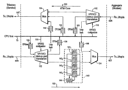
2.0 ATM Core
to Fig, 2 shows generall;~ the structure of ATM core 60. In Fig. 2, internal
CPU bus
73 serves to divide ATM core 60 into a downsteam side (above bus 73 in Fig. 2)
and an
upstream side (below bus 73 in Fig. 2 ).
The downstream side of ATM core 60 includes a downstream demultiplexer and
translator I02 which has an input tercninal connected to the receive portion
62R of
t s modemltransceiver interface 62. Differing output terminals of downstream
demultiplexer and translator 102 are connected to a downstream multiplexer
104; .,
downstream read CPU buffer 106; arid downstream loop-back buffer 108. The
downstream read CPU buffer 106 is connected to internal CPU bus 73. Internal
CPU
bus 73 is also employed to provide VPI/VCI configuration information to
downstream
2o demultiplexer and translator 102 as indicated by line 110.
Downstream multiple;xer 104 has differing input terminals connected to an
output terminal of downstres~m demu~ltiplexer and translator 102 as described
above, as
well as to a set 116 of downstream write CPU buffers and to an upstream loop-
back
buffer 118. An output terminal of downstream multiplexer I04 is connected to a
25 transmit portion 647 in services inter~face 64.
CA 02284175 1999-09-10
2.SEP.1999 13:19 DEPARTMENT FOR IPR NR.326 S.13i29
WO 99137tI7 PCTlSE98/02466
The upstream side o~f ATM core 60 includes an upstream demultiplexer and
translator 122 and an upstream multiplexes 124. A first input terminal of
upstream
demultiplexer and translator 122 is connected to a receive portion 64R of
services
interface 64. A second input terminal of upstream demultiplexer and translator
122 is
s connected to ups eam write CPU buffer 126. The VpINCI tables of upstream
demultiplexer an translator 122 are updated by CPU 40 as indicated by line
120.
Differing output erminals of upstxeam demultiplexer and translator 122 are
connected
to upstream loop back buffer 118; a set 136 of upstream CPU write buffers; and
(via
buffer section 14p) to upstream mulriplexer 124.
to A first input terminal of upstream multiplexes 124 is connected to
downstream
loop-back buffer I~108. A second input terminal of upstream multiplexes 124 is
connected to out~uts of buffer section 140. An output terminal of upstream
multiplexes
124 is connected 'Ito a transmit portion 62T in modetn/tra.nsceiver interface
62.
j
Buffer section 140 includes plural internal queues, e.g., for differing types
of
is service quality. Ian the illustrated embodiment, buffer section 140
includes first through
forth buffers nu ~bered as 1421 through 1424, respectively. Cells input to
buffer
section 140 are r uted to an appropriate one of the queues 1421 through 1424
depending, e.g., n their qu~ility of s<;rvice.
In addition, an early ;packet discard (EPD) 144 is also provided as part of
zo upstream demultiplexer and translator I22. When a sequence of cells that
together form
a PDU (Packet D~ta Unit) is about to be stored in a queue or buffer, it is
possible to
decide that the complete PD~U shall be discarded. Discarding of the complete
PDU may
be necessary, for example, if the queue or buffer has insufficient space to
accommodate
the complete PD . Rather ~:han storing only a part of the PDU, the complete
PDU is
2s discarded. The particular illlustration of early packet discard (IrPD) 144
in Fig. 2, for
example, is intended to indicate that a cell which otherwise would be stored
in one of
CA 02284175 1999-09-10
2.SEP.1999 13:20 DEPRRTMENT FOR IPR NR.326 5.1429
t
WO 99/37117 PCT1S~98102466
11
the queues I42I through 142:4 is subject to early packet discard by upstream
demultiplexer and translator 122.
As explained in more detail hereinafter, in the downstream direction depicted
as
arrow I50 in Fig. 2, cells obizined from modemltransceiver 22 are distributed
either to
s one of the service devices 701, 702, i'2, and 74 or to downstream read CPU
buffer 106.
Cells can also be read from <_;e~t I 16 of downstream write CPU buffers and
sent to
service devices 701, 702, 72, and 74. In the upstream direction depicted as
arrow I52 in
Fig. 2, ATM core 60 reads A.TM cells from service devices 701, 702; 72; and 74
and
distributes the cells either to the set 136 of upstream CPU write buffers or
to
~o modem/transceiver 22. Cells can also be read from upstream write CPU buffer
126 and
sent to modem/transceiver 2'2.
3.0 Cell Flow
3.1 Downstre;3m Cell Flow
As soon as portion 6=;R of modem/transceiver interface 62 has a cell
available,
is the cell is read and the VPhVCI of tt~e incoming cell is examined by
downstream
demultiplexer and translator 102. In this regard, downstream demultiplexer and
translator 102 has VPINCI tableswhich is configured by CPU 40. These VPIlVCI
tables are described in more detail with reference to Fig. 17A.Based on the
VPIIVCI of
the incoming cell, a look up operation is performed in the VPI/VCI tables of
2o downstream demultiplexer ~~nd translator 102 to determine both the physical
destination
of the cell, as well as what new VPIlVCI the cell should haveas it leaves ATM
core 60.
Fig. 2A shows in more detail a downstream side of ATM core 60, and
particularly illustrates more fully the set 116 of downstream write CPU
buffers. As
shown in Fig. 2A, the set 116 of downstream write CPU buffers includes buffers
1161,
2s 1162, and I 163, each of which have input terminals fed by internal CPU bus
73 and
output terminals connected to an input tenyninal of downstream multiplexer
104. Each
ofthese buffers is associated with one of three of service devices 741, 702,
?2, and 74,
CA 02284175 1999-09-10
2.StP.1999 13:20 DEPARTMENT FOR IPR NR.326 S.15i29
WO 99/37ii~ PCT/St=98102466
12
thereby giving ATM core 6~0 the abil'.ity to send cells from CPU 40 to the
three service
devices having one of the buffers 1161, 1162, and 1163.
Fig. 3A, in conjunction with Fig. 2A, shows the general steps performed by
downstream demultiplexer I02 in handing a cell incoming from
modernltransceiver 22.
s At step 3A-1 demultiplexer 102 determines whether a cell is available from
modemltransceiver 22 on interface 62. Cells available from modern/transceiver
22 on
interface 62 are known as ";aggregate" cells. DemuItiplexer 102 repetitively
checks
whether an aggregate cell is available, as indicated by the negative branch of
decision
symbol of step 3A-1. If an aggregate cell is available, at step 3A-2 its
VPI/VCI is
to examined (as described above) and downstream multiplexer 104 is halted.
Based on
VPI/VCI, downstream dem~~ltiplexer. and translator 102 knows where the cell is
headed
e.g., for one of service devices 701, '702, 72, and 74, or for CPU 40 (e.g.,
downstream
read CPU buffer 106), or for downstream loop-back buffer 108. In this regard,
see
Section 10.1 and Fig. I 7A.
is After the VPINCI o,f the downstream incoming cell is translated, a check is
first
made at step 3A-3 whether the cell is headed for CPU AO and whether downstream
read
CPU buffer 106 is ready to receive a. cell. If the check at step 3A-3 is
affirmative, at
step 3A-4. the cell is writteA to downsrream read CPU buffer 106.
If the determination at step 3A-3 is negative, a check is made at step 3A-5
2o whether the cell is headed for down:;tream loop-back buffer I08, and
whether
downstrearn loop-back buffer 108 is ready to accept a cell. If the check at
step 3A-5 is
affirmative, at step 3A-6 th~~ cell is sent to downstream Loop-back buffer
108.
If the determination at step 3.4-5 is negative, a check is made at step 3A-7
whether the cell is a Utopia cell (e.g., is headed for one of the service
devices 701, 702,
2s 72, and 74) and whether th~~ particular device to which the cell is headed
is ready to
accept a cell, If the check at step 3A-7 is affirmative, at step 3A-8 the
attention of
CA 02284175 1999-09-10
2.SEP.1999 13:20 DEPRRTMEN1' FOR IPF', NR.326 S.16i29
w0 99/39117 PCTISE98102466
I3
downstream multiplexes 104. is requested. The attention of downstream
multiplexes 104
is repetitively requested until it is determined (at step 3A-9) that
downstream multipexer
104 is ready. Once downstream multiplexes 104 is ready, at step 3A-IO the cell
is sent
to downstream multiplexes l, 04 so that the cell can be sent over the transmit
portion 64T
s of services interface 64 to the particular device to which it is destined.
Regarding the check of step 3.A-7, ATM core 60 is continuously updated
regarding the buffer status fir each of the service devices 701, 702, 72, and
74. In this
regard a polling using the T:{ Clav signal over interface 64 provides an
indication
whether there is sufficient space in the buffer of each device for storing a
complete cell.
io If the determinations at steps ;3A-3, 3A-5, and 3A-7 are all negative, the
cel! is
discarded as indicated by step 3A-11. Upon completion of each of steps 3A-4,
3A-6,
3A-10, and 3A-11, execution continues with the awaiting ofprocessing a new
downstream cell at step 3A-1.
Fig. 3B, in conjunctiion with 'Fig. 2A, shows the general steps performed by
~5 downstream multiplexes 104. Step'.~B-1 shows multiplexes 104 determining
whether it
hays been halted by demultiylexer 10;? (see step 3A-2 of Fig. 3A). If
multiplexes 104 has
been halted, at step 3B-2 a determination is made whether a cell is available
from
demultiplexer 102. Multiplexes 104 knows that a cell is available from
demultiplexer
102 when demultiplexer 102 has requested the attention of multiplexes 104 (see
step
20 3A-8 of Fig. 3A). If a cell is not available from demultiplexer 102,
multiplexes 104
loops back to step 3B-1. If a cell is available from demultiplexer 102, at
step 3B-3 the
multiplexes 144 receives the cell which was sent to it by demultiplexer 102
(see step
3A-10 of Fig. 3A). Then, a.t step 3E.-4, multiplexes 104 gates the cell to the
appropriate
one of the Utopia devices (service devices 701, 70~, 72, and 74) as indicated
by the
2s VPI/VCI of the cell. After the gating of the cell, operation loops back to
step 38-1.
CA 02284175 1999-09-10
2.SEP.1999 13~21 DEPARTMENT FOR IF'R NR.326 5.1729
WO 99/37117 PCT/SE98IOZ466
14
If multiplexes 104 has not been halted by demultiplexer 102, at step 3B-~
multiplexes 104 checks whether a loop back cell is available from upstream
loop-back
buffer 118. If a cel! is available from upstream loop-back buffer 118, at step
3B-6 a
check is made whether the appropriate Utopia device (one of service devices
701, 702,
s 72, and 74) to which the cf~ll is destined is ready to accept the cell- If
the service device
is not ready, operation returns to stf;p 3B-1. If the service device is ready,
at step 3B-7
the multiplexes 104 reads the cell from upstream loop-back buffer 118, and at
step 3B-8
the cell is gated through multiplexes 104 to the appropriate service device.
After the
gating of the loop back cell through multiplexes 104 to the appzopriate
service device,
~o operation loops back to step 3B-1.
If a loop back cell is not available from upstream loop-back buffer 118, at
step
3B-9 a determination is made whether a CPU cell is available from one of
downstream
write CPU buffers 116. If none of i:he buffers 116 have a cell available,
operation loops
back to step 3B-1. If one of the buffers 116 does have a cell available, at
step 3B-10 a
is check is made whether the Utopia device (e.g., one of service devices 701,
702, 72, and
74) to which the CPU cell is destined is ready. If the servicE device is not
ready,
operation loops back to step 3B-1. If a CPU cell is available, at step 3B-11
the CPU
cell is read from the ready one CPL:I buffers I 16. At step 38-12 multiplexes
104 gates
the CPU cell to the appropriate sen,~ice device, after which operation
continues at step
Zo 3B-1.
The operations of demultiplexer 102 as described in Fig. 3A and the operation
of
multiplexes 104 as described in Fia. 3B are such that these devices can handle
cells
independently at the same time. For example, if demultiplexer 102 is busy
reading cells
from interface 62 and storing the read cells in downstream Ioop back buffer
10$,
i5 multiplexes 104 can read cells from upstream loop-back buffer 118 and send
such cells
to one of the service devices 701, 702, 72, and 74. Only if cells are going
from
interface 62 to interface 6~E must both demultiplexer 102 and multiplexes 104
work
together.
CA 02284175 1999-09-10
2.SEP.1999 13:21 DEPARTMEN-f FOR IPR NR.326 S.18i29
wo 99/3717 PCTISE98ro2a66
IS
3.2 Upstream Cell Flow
Fig. 2B shows in more detail an upstream side of ATM core 60, and particularly
illustrates more fully the set 136 of upstream CPU write buffers. In
particular, the set
136 of upstream CPU write buffers includes buffers 1361, 1362, and 1363. Each
of
s these buffers is associated with one of three service devices 701, 702, 72,
and 74,
thereby giving ATM core 6(~ the abilaty to send cells to CPU 40 from the three
service
devices having one of the buffers l3EiI, 1362, and 1363.
On the upstream side of ATM core 60, the service devices service devices 70I,
702, 72, and 74 on services ;uterface 64 are read as soon as one of them has a
cell
io available. Ceil availability is denoted by the Rx Clav signal specified on
interface 64.
Besides the services interface 64, upstream write CPU buffer I26 is also read
when it
contains a complete cell. The service; devices and upstream write CPU buffer
126 have
the same priority.
In the upstream direction, there are eight possible destinations for incoming
is upstream cells -- the three buffers in set I36 of upstream CPU write
buffers, the four
buffers in buffer section l4Ci, and up stream loop-back buffer 118. VPWCI
cannot
solely be relied upon to determine the destination of the incoming upstream
cells. The
fact that two cells from diffE~rent ATMF channels have the same VPI/VCI means
that
the physical source {e.g., A'',CMI= interface 701, 702) must also be used to
determine the
2a destination. In like manner as downstream demultiplexer and translator 102,
upstream
demultiplexer a.nd translator 122 has VPI/VCI tables which also includes
source
information. The VPI/VCI tables of upstream demultiplexer and translator I22
are
updated by CPU 40 as indicated by line 120. The VPI/VCI tables of upstream
demultiplexer and translator 122 are' described in more detail in section 10.2
and Fig.
25 I7B.
Because ATM core ti0 quickly reads cells and stores cells in the destination
buffers, ATM core 60 can always make sure that the different serYice devices
arc read
CA 02284175 1999-09-10
2.SEP.1999 13:22 DEPf~RTMENT FOR IPR NR.326 S.19i29
WO 99f37117 PCT/SE98/02466
16
in proper order. In this regard, ATM core 60 works sufficiently quickly that,
even when
data is received at maximum speed from all service devices, there is no risk
that any of
the service devices 701, 70~;, 72, and 74 will be blocked.
Early packet discard can be performed for all ATM connections and for all
buffers in buffer section 140. For each VPINCI there is information whether
early
packet discard (EPD) is to >r~e performed or not (in accordance with
configuration by
CPU 40 at connection set up) and the current EPD status (an internal
variable).
Cells in buffer section 140 are multiplexed together with cells from
downstream
loop-back buffer 108 at upstream multiplexer 124 for application to
modem/transceiver
interface 62.
On the upstream side: of ATN( core 60, a cell is obtained as soon as
modem/transceiver interface 62 indicates that it is ready to receive a
complete cell.
When such an indication is received at upstream muitiplexer 124, cells) in
downstream
loop-back buffer 108 is given highest priority, and can be connected to any of
the four
1s channels on modem/transceiver interface 62. The handling of the buffers in
buffer
section 140 depends on the mode of ATM core 60. There are three different
modes of
ATM care 60.
In a first mode of A''CM core 60, all four buffers 1421 - 1424 in buffer
section
140 are connected to one channel or.~ modemltransceiver interface 62. In this
first mode,
2o all four buffers 1421 - 142q. have dii:ferent priorities.
In a second mode of ATM care 60, two buffers 1421 - 1422 are connected with
one channel on modemltrmsceiver interface 62 and two other buffers 1423 - 1424
are
connected with another chaunnel on tnodemltransceiver interface 62. In this
second
mode, the two buffers connected with the same channel have different
priorities, but
CA 02284175 1999-09-10
2.SEP.1999 13:22 DEPRRTMENT FOR IPR NR.326 5.229
WO 99/37119 PCT/SE98/02466
I7
they have the same priorities; as the two other buffers that are connected to
the other
channel.
In a third mode of ATM core 60, each of the buffers 1421 - 1424 are connected
with a separate (e.g., different) one ofthe channels on modemltransceiver
interface 62.
s In this third mode, all four buffers 1421 - 1424 have the same priority.
4.0 VPI/VCI Handling
Each ATM connection has two VPI/VCIs -- one for the connection on the
modemltransceiver interface. 62 (e.g.., on the aggregate side), and another
for the
connection to and from service interface 64 (e.g., on the tributary side),
Because
to upstream cells from circuit emulator 72 are created with a fixed VPI/VCI,
this fixed
VPI/VCI value must be used for the tributary VPIIVCI. The translation of
VPI/VCI
values using VPINCI tables, is discussed in section 10.0, as well as Fig. I7A
and Fig.
17B. Examples of ATM coanection:~ are shown in Table 1.
ATM core 60 can hactdle a total of 128 simultaneous ATM connections, both
t5 VPCs and VCCs. On the aggregate side, all twelve bits of the VPI are used,
but only
sixteen combinations can be valid simultaneously, The eight most significant
bits are
used for filtering cells, which is necessary in an HFC application where each
NT must
have its own VPI. The four least significant bits (sixteen combinations) will
determine
the VPC/VCC (together with the VCI for VCCs). In an ADSL application, the
eight
2o most significant bits can be reset. Only eight bits of the VCI are used
(the LSBs). All
256 VCI combinations and the sixtef;n VPI combinations can be mixed, but only
128
combinations can be valid simultaneously.
On the tributory side, only four bits of the VPI are used (the least
significant bits)
and only eight bits of the VCI are used (the least significant bits). All
combinations can
2s be mixed, but only 128 corr,~binations can be valid simultaneously.
CA 02284175 1999-09-10
2.SEP.1999 13~22 DEPRRTMENT FOR IPF'. NR.326 S.21i29
w0 99/37117 PCTiSE98/oZa66
18
Fig, 4A shows how f~ VP cross connection can be set up through ATM Core 60.
Fig. 4A includes a demux aad translation table 400 which is stored in a set of
internal
RAMS in ATM core 60 and which are maintained by CPU 40. Any of the I28
connections through ATM core 60 ran be configured as VP cross connections
(VPC),
s with sixteen of such connections being configured simultaneously as VPC. In
that case
the 4 LSB's of the VPI is miaslated. The 8 MSBs at the aggregate side must
correspond
to the VP filter, and at the tributary side they a.re reset, i.e. no generic
flow control
(GFC) handling is supported. All VC's belonging to a VPC are transparent
except for
OAM; Segment and end-to-end F4 slows are sorted out and send to CPU 40.
to
Fig. 4B shows how'~lC crass connections can be set up through ATM core 60.
All I28 simultaneous connections through the ATM core 60 be configured as VC
cross
connections (VCC). Using VCC handling means that only VC's that are defined in
the
demux- and translation table are distxibuted through ATM core 60, including
pre-
is defined signalling VC's (V(~=5 for TTU and VC=16 for ATM Forum as shown in
Fig.
4B). The 8 MSBs of the VC'I must be 0. Both the 4 LSBs of the VPI and the 8
LSBs of
the VCI are translated. The 8 MSBs of the VPI are handled as for VP cross
connections. Segment and end-to-end F4 OAM cells are sorted out per VP, just
like for
VPCs. However, segment h5 cells are sorted out per VC. Those cells are send to
CPU
20 40.
In an HFC application, ability to broadcast cells is needed. This is provided
with
a separate VPI register 402 as shown in Fig. 4A and Fig. 4B. Downstream cells
with a
VPI that corresponds to thi:~ register will be send to the CPU.
2s 5.0 Buffering
Quality of service (CI.oS) handling is handled only for the upstream flow. All
cells that are read from the services interface 64 (and set 136 of upstream
CPU write
CA 02284175 1999-09-10
2.5EP.1999 19:23 DEPARTMEN1' FOR IPF? NR.326 S.22i29
WO 99137117 PC'TISE98~02466
19
buffers) and are heading for upstrearn transportation (the direction of arrow
1~2 in Fig.
2) are stored in the buffer section 140.
Buffer section 140 of mufti-service circuit 20 is shown in more detail in Fig.
5.
s Buffer section 140 actually comptis~a a buffer controller 140C which is
connected
between upstream demultiplexer and translator 122 (the tributary mux) and
upstream
multiplexes 124 (the aggreE;ate mux;~. Buffer controller 140C supervises data
retrieval
and storage either in internal memory (e.g., RAM 142) or in an external memory
(e.g.,
SRAM 142X shown in Fig. 1). For example, the buffers 1421 - 1424 shown in Fig.
2
to and Fig. 2B can be included in intenzal memory (e.g., RAM I42). Whether
buffers
1421 - 1424 are included in~ internal memory or external memory is specified
and
allocated by CPU 40 at start up.
Thus, mufti-service circuit 20 has a limited internal buffering capacity,
indicated
is by the four queues 1421 - 1424. In the illustrated embodiment, the size of
the internal
memory is 2048 x 8. The size of external SRAM 142X is much larger, e.g., 128K
x 8.
As shown in Fig. 5~~, either internal memory 142 or external memory 142X is
divided into 4 areas. As e~:plained above, these four areas can correspond in
some
2o modes of the invention to differing cell classes. The first area (Area 1)
always starts at
address 0x0000, with Area 2 - Area 4 being subsequently provided. The size of
all
areas is programmable, including th.e EPD threshold values for all areas. As
mentioned
above, in view of differing operating modes, the four buffer areas Area 1 -
Area 4 need
not necessary correspond to four different QoS classes. Two constant bit rate
(CBR)
25 cells can be stored in different buffer areas if one is more timing
critical than the other.
This is decided at set up fc~r each ATM connection.
CA 02284175 1999-09-10
2.SEP.1999 13 23 DEPARTMENT FOR IPF2 NR.326 S.23i29
w0 99137117 PC'T/SE98/02466
6.0 Circuit Emulation Device:
Circuit emulation (C:E) device 72 performs conversion between ATM and
synchronous telephony trafi:ic. In the upstream direction (see arrow 152 in
Fig. 2),
circuit emulation (CE) device 72 pac;ketizes the synchronous timeslot traffic
from the
s PCM interface into ATM cells via A.AL1 (adaptation layer 1). The cells are
put onto
the services interface 64 for further upstream transportation. In the
downstream
direction (see arrow 150 in '.Fig. 2), incoming ATM cells from services
interface 64 are
unpacketized and the timeslot traffic is reconstructed, this is also done via
AA.L 1.
io One context of circuiit emulation (CE) device 72 is shown in Fig. 6,
wherein
circuit emulation (CE) device 72 is connected between services interface 64
and PCM
interface 32. Line circuitry 36 (see I=ig. 1) includes a dual subscriber line
audio circuit
(DSLAC) which connects to several subscriber line interface circuits (SLICs).
A SLAG
is a circuit that takes care oi'PCM modulation, and is also referred to as a
CODEC
is (COderIDECoder). A DSL.AC has two SLACs in one circuit. A SLIC handles the
high
voltage and current on the subscriber line.
Fig. 6A shows example architecture of circuit emulation (CE) device 72.
Circuit
emulation (CE) device 72, Like all of mufti-service circuit 20, is a pure
hardware circuit.
2o Circuit emulation (CE) device 72 ha.s a set of configuration and status
registers 72-10
which are connected by internal CP1:J bus 73 to CPU 40, Usage of registers in
set 72-10
are described below. Circuit emulation (CE) device 72 has a PCM Elrf 1
interface 72-
20 which connects to interface 32; a nAALl reassembly unit 72-30 which
connects to
transmit lines in interface 64; and, an A.AL1 segmentation unit 72-40 which
connects to
is receive lines in interface 64~. Between PCM interface 72-20 and AALI
reassembly unit
72-30 is a downstream dual. port RANT 72-~0. Beriveen PCM interface 72-20 and
AAL 1 segmentation unit 7 2-40 is an upstream dual port R.AM 72-60, Each of
the dual
port RAMs 72-50 and 72-60 is divided into different areas as hereinafter
described.
CA 02284175 1999-09-10
2.SEP.1999 13 24 DEPRRTMENT FOR IPR NR.326 S.24i29
WO 99!'37117 PC'TISE98J02466
21
6.1 Packetization
The telephony data car. be packetized into either structured 64 kbps channels
or
unstructured 2048/I544 kbps channels. Both methods are described below.
6.1, I . Structured 64 kbps channels
For structured 64 kbps channels,, the ATM cells will always contain data from
only one channel. The cells can either be totally filled (47 octets} as shown
in Fig.
6B(1), or partially filled (22 or 11 octets) as shown in Fig, B(2). The
benefit with
totally filled cells is the high utilization of the bandwidth (100%), and the
drawback is
the high assembly delay (47 x 125 ms =5.9 ms). The bandwidth utilization for
partially
filled cells is lower (47% for :?2 octets and 23% for 11 octets), but the
assembly delay is
also lower (2.8 ms and 1.4 ms respectively),
6.1.2 Unstructured 201~8/1544 kpbs channels
When using unstructured 2048/1544 kpbs channels, the ATM cells contains data
from all channels from either a E1 interface (2048 kbps) (see Fig. 7A] or a T1
interface
(1544 kbps) [see Fig. 7B].
6.2 Celi Delay Variation
2o The data traveling dov~~nstream (e.g., in the direction of arrow 150 in
Fig. 2) must
be additional delayed in order to handlie cell delay variation (CDV). As shown
in Fig.
8, there is a nominal transmission delay from the source to the destination.
If that delay
were constant, the destination, could start reading data just after the moment
the cells
has arrived. However, some .cells could be more delayed than others, so the
destination
must have an extra buffer in the case F~ cell is very late, Otherwise, there
will be buffer
underflow. Because of the large assernbly delay, not much extra delay can be
added for
CDV handling. In the illustr~ited embodiment, circuit emulation (CE) device 72
handles
up to 3.9 ms CDV.
CA 02284175 1999-09-10
2.SEP.1999 13:24 DEPfaRTMENT FOR IPR NR.326 S.25129
WO 99/3711? PCT/SE98/024G6
22
6.3 Lost and Misins~erted Cells
By looking at the sequence number in the SAR-PDU header, lost and misinserted
cells can be detected. When a cell appears with a sequence number that is not
in
sequence with the previous one, it could be a misinserted cell but it could
also be a
number of lost cells between this and the previous cell, This can be
determined by
looking at the sequence number of the next cell. If it is in sequence with the
present
one, it is considered that some cells have been lost. If it is in sequence
with the
previous one, the present one is misi.nserted. A cell which is not in sequence
will NOT
1o be stored. If the cell is considered a:; misinserted (afrer the next cell
has arrived), there
is no harm done of not storing the cell. If cells have been lost, the harm is
done
anyway.
6.4 Synchronizatior.~
is Because POTS is a :synchronous service, it is necessary that a service
clock
related to the source be recovered, otherwise there will be buffer overflow or
underflow.
In a synchronous system, the service clock is extracted directly from the
network clock
(the downstream data clock. from the; modem), In an asynchronous system,
adaptive
clock extraction is usually used. However, this method is not suitable for
structured
2o circuit emulation because of the delay. Instead a reference clock is
provided from the
modem, which is used to g<;nerate an own clock.
6.5 Segmentation
The data from each POTS channel is typically a constant octet flow with a
25 periodicity of 125 ms. The octets are stored in a buffer -50 in consecutive
order. The
buffer has 94 octet positions per POTS channel, which covers two cells for
totally filled
mode (Fig. 9A), 4 cells for 22 octet-partially filled mode (Fig. 9B), and 8
cells for 11
octet-partially filled mode (:Fig. 9C).
CA 02284175 1999-09-10
2.SEP.1999 13 24 DEPRRTMENT FOR IPR NR.326 S.26~29
WO 99~37I17 PC?/SE98/02466
z3
6.5.1 Segmentation: 64 Kbps Bearer Cells (totally filled)
When the circuit emulation (Cl~) device 72 is working in a mode of 64 kbps
bearer-cells, the buffer is configured to have two areas of 47 octets each
(Fig. 9A).
s Each area represents a cell - the first area (octets 0 to 46) represents
cells with even
number, the other area (octec~ 47+) represent cells with odd number. CPU 40
controls
the start of each channel by setting a dedicated bit in the configuration
register.
Channels that are using single 64 kbp,s bearer are initialized independently
of each
other. As soon as one area h;ls been filled with data from the PCM interface,
a cell can
to be created and sent upstream. Because there is no extra cell buffer, the
cell is not
created until the device that controls the Utopia interface 64, i.e., the ATM
core 60,
requests a cell. ATM core 60 requests a cell shortly after it has received an
indication
that a cell is ready, which really means that a cell is ready to be created.
When a cell is
created, the 47 octets of PCIvi data arf: put into the SA.R-PDU payload, and a
sequence
is number is put into the SAR-1'DU header.
6.5.2 Segmentation: 64 kbps Bearer Cells (22 Octets)
When 64 kbps bearer~cells, partially filled with 22 octets, are employed, the
buffer is configured to have ~l areas of 22 octets each (Fig. 9B). A.s in the
preceding
2o discussion, each area (e.g., A.rea 1 - Area 4) represents one cell: the
first area (octets 0 -
21) represents cells with sequence number 0 and 4, the second area (octets 22 -
43)
represents cells with sequence number 1 and 5, the third area (octets 44 -
fi5) represents
cells with sequence represents number 2 and 6, and the fourth area (octets 66 -
87)
represents cells with sequence represents number 3 and 7. Even here the CPU is
2s enabling the start of the writing into the buffer. When a cell area is
filled with data (22
octets), indication is given that a cell can be created. A cell is created in
the same way
as described above, but only 22 octets are put into the SAR-PDU payload. The
remaining 25 octets are dummy octets.
CA 02284175 1999-09-10
2. ST=P.1999 13 25 DEPARTMENT FOR IPR NR.326 S.2?i29
w0 99137117 PCTISE98I02466
24
6.5.3 Segmentation: 64 kbps bearer Cells ( 11 Octets)
When 64 kbps bearer-cells, partially filled with 11 octets, are employed, the
buffer is configured to have 8 areas of 11 octets each. As in the previous
modes, each
s area represents a cell. But in this scenario each sequence number has a
unique area.
The CPU enables the start o~~the buffer writing, even though this is not very
critical
because of the low assembly delay. '.Che creation of a cell is similar to the
next
previously discussed mode, except that the number of dummy octets (36) differs
~0 6.5.4 Handling of several simultaneous single 64 kbps bearer
In order to handle t<vo 64 kbp;~ channels simultaneously, the 94-octet buffer
must
be doubled as shown in Fig. 9D. For the part that takes care of the writing
into the
buffers, this will not make any difference. Each channel is stored
independently of each
other. For the part that taker care of the cell creation, each buffer is
treated as a
1s different cell flow (which it is). When a cell for channel 1 is ready to be
created, this is
indicated to services interface 64 on a separate signal. For channel 2,
indication is
given on another signal. The services interface 64 requests a cell from the
two channels
separately. For 4 channels E~ buffer of 4 x 94 octets are needed, as shown in
Fig. 9D.
20 6.5.5. Packetizing of unstructured E1/Tl frames
E 1 (2048 kbps) and 7.'1 ( 1544 kbps) frames are transported unstructured over
ATM, i.e. the data is packetized into totally filled cells without any
handling of separate
64 kbps channels. Because of the serial interface, there is no need for any
alignment of
the data. In this mode the buffer is configured according to Fig. 9E. In this
mode the
2s buffer is filled with data much faster than the n x 64 kbps modes, which
means that the
initialization of the writing :is not very critical.
CA 02284175 1999-09-10
2.SEP.1999 13~25 DEPARTMENT FOR IPR NR.326 S.28i29
WO 99/37117 PCTISE98/02466
6.6 Reassembly
For the reassembly function, the: same respective buffers are defined as for
segmentation function. Moreover, the buffers will also have the same
configurations as
for the respective segmentation functions.
s
6.6.1 Unpacketizina
The unpacketizing of tile different cells follows the same behaviour as for
the
packetizing. The cells are received from services interface 64. If several
single 64 kbps
bearers are used, the channels are separated with different enable signals.
When a cell
to is received, the user data is stored in th.e dedicated area in the bufFer
(determined by the
sequence number). This is also indicated to the read side, so it can see
whether data has
been written into the area since last tune it was read. The buffer is
continuously read in
a consecutive order, and the data flow is send to the PCM interface 32 - one
channel per
buffer. Fig. 10 shows unpack.etizing of t<vo partially filled single 64 kbps
bearer-cells.
is
6.6.2 Handling of Lost and Misinserted Cells
When a cell is received at circuit emulation (CE) device 72, the sequence
number
in the SAR-PDU header is checked. If a cell Ct is not in sequence with the
previous cell
Ct_l, it is discarded and the user data is not stored. If the next cell Ct;.l
is in sequence
2o with cell Ct_1, cell Ct is considered as misinserted and the reassembly
procedure
continues. If cell Ct-~-1 is in sequence with cell Ct, it is considered that a
number of
cells have been lost between cell Ct_1 and cell Ct. Even in this case the
reassembly
procedure will continue, resulting in that cell Ct is discarded even though it
is a correct
cell. However, a possible misinserted cell can not be stored because the
buffer will only
25 have place for two cells when using totally filled cells. An example is
shown in Fig. 11.
If the buffer area for cadd cells is being read and a misinserted cell with an
odd
sequence number arrives Ct, the payload must not be stored in the area that is
currently
CA 02284175 1999-09-10
2.SEP.1999 13-25 DEPARTMEN1- FOR IPF? NR.326 S.29i29
' w0 99139117 PCTISE98I02466
26
being read. Because of the small buffer size, there is no possibility to
insert the
recommended dummy data into the buffer instead of lost cells. However, each
time a
cell payload is written into the buffer, this is indicated to the read side.
If there is no
indication that a cell has been written into an area since last time it was
read, the read
side will generate the necessF~ry number of dummy bits (ls).
6.6.3 Handling of Cell Delay Variation (CDV)
If all cells had the same delay through the network, they should appear with a
precise periodicity. In that c,ise, the read part could start reading the
buffer the moment
to after the first cell has arrived. In reality, some cells will have more
delay (see Fig. 8),
which could mean that a bufirer area is read before it has been filled with
data (buffer
underflow). Therefore the read part should be delayed initially when the first
cell
arrives, so that it will continuously resid each cell area a certain time
after the cell has
been written into it. In that r,ase it will not be buffer underflow if a cell
suddenly arrives
is a little late. The extra CDV .delay is programmable by the CPU.
6.7 Synchronization
Mufti-service circuit 20 needs an 8 kHz network reference clock in order to
synchronize the telephony flow. A phase locked loop (DPLL) is used to generate
a
2o clock that is locked to the re Perence clock, as shown in Fig. 12 for
synchronization of
the downstream data rate. V~~hen interface 32 is a PCm interface, the
oscillator
frequency (fosc) must be 32.768 MHz and the generated clock (flck) is 2.048
MHz.
This is the same for the EI interface. However, if the Tl interface is to be
used, fosc is
24.704 MHz and flck is 1.54.4 MHz. The oscillator is external.
6.8 Interfaces and Clocks
Circuit emulation (Ch) device. 72 is connected to interface 32, services
interface
64, and internal CPU bus 73~. Circuit: emulation (CE) device 72 is divided
into two
CA 02284175 1999-09-10
._:.~~-1~ 13 ~ 27 DEP~~TT1ENT FC~R IPR S. Ii43 . =: ~ :.,~«, -;-,:-:~
_.
.; ~ a:>.~ .x::;z.'F.:.:;
WO 99r311iT PCF/SE98I02466 .
. . . .:. ;
z~
clock areas. The handling of ATPd cells (distribution of data etwecn buffer
and
services interface 64 is clocked bar the clock that is distributed from the
services
interface 64 (the system clock), C)n the other hand, the handling of telephony
data
(distribution of data between the hCMIEi/Tl interface and the buffer) is
clocked by the
DPLL clock (see Fig. 12).
7.0 Utopia Buffer
Utopia buffer 74, shown ire Fig. 13, is basically a bu~'er between services
interface 64 (an internal tributary Utopia imterface), which is controlled by
ATNI core
to 60, and an external service Utepi~~ interface 34 which is controlled by the
external
device that is connected to it. Th~= interna',~ buffers in utopia buffer 74
can store 2 cells
per direction. The e.~cternal Utopia interface 34 can work in either level 2
or level 1
mode, the mode selection being configured by CPU ~0 at start up. In level ?
mode, the
physical address must also ~be configured. Utopia buffer 74 has three
different clocks.
t5 Distribution of data between utoF~ia buffer 74 and the internal tributary
interface
(services interface 64) is clocked by the system clock. Distribution of data
between
utopia buffer 74 and the external Utopia interface 34 is clocked by t<vo
separate clocks
for transmit and receive, both such clocks being provided :rom the external
Utopia
interface 34.
8.0 ATMF 2~.6 Transceivers
ATMF transceivers 701, i'0~ are each a point-to-point physical ATM interface
for a twisted pair cable, as specified by A'TM Forum. The ATMF 25.6 Mbps
transceivers 701, 702 are a common standard interface and are provided by
computer
2s plug-in cards and set-top-boxes (STB). A representative one of the ATMf
transceivers
701, 702 is shown as transceiver 70 in Fig. 14.
In the downstream direction (shown by arrow 150 in Fig. 2), cells are received
at
ATvLF transceivers ~O l, 70~ from the se;cvices interface 64 and are
transmitted on the
CA 02284175 1999-09-10
2.SEP.1999 13 27 DEPARTMENT I=OR IPR NR.327 S.2i43
WO 99/37117 PG?ISE98/02d66
28
25.6 Mbps lines 301, 302 after having been temporarily stored in a two cells-
deep
FIFO. In the upstream direction (depicted by arrow 152 in Fig. 2), ceps are
received
from the 25.6 Mbps lines 301, 302 and are stored in a two cells-deep FffO,
where they
can be read by the ATM core ti0. The ifilnctions of the Physical Media
Dependent
s (PMD) sublayer and the Transoaission Convergence (TC) sublayer are specified
in the
ATM 25.6 Mbps Physical Interface Specification from ATM Forum. An 8 kHz
reference signal is provided to the downstream part (the same signal as for
the DPLL of
circuit emulation (CE) device '12), so that timing information can be
transmitted over
the ATMF interface 30. The downstream clock is distributed from an external 32
MHz
to oscillator. The upstream clock. is extracxed from the upstream flow. 'The
handling of
cells between the FIFOs and tree services interface (i4 is clocked by the
Utopia clock
(the system clock).
9.0 CPU Block
is The CPU block 71 distributes data between (1) the external CPU bus 42 and
(2)
ATM core 60 and service devices 701, 702, 72, and 74. CPU block 71 also
handles
interrupt. All functions performed by C;PU block 71 including the transactions
over the
internal interface (e.g., bus 73) are clocked by the system clock.
ao 9.1 Read and Write Handling
Reading and write handling as performed by CPU block 71 are illustrated in
Fig.
15. When the CPU 40 performs a read or write action to mufti-service circuit
20, the
CPU block 71 detects a low transaction on the chip select signal (CS). CPU
block 7I
then decodes the address bus and distributes the least significant bits of the
address bus
2s and a block select signal to the selected. block (e.g., ATM core 60 or one
of service
devices 701, 702, 72, and 74). Bus 73 is a bidirectional data bus which is
diverted into
two separate buses for read an~3 write. 'When the internal read or write
action has been
finished, this is indicated by th.e data transfer acknowledge signal. Since
the read or
write action is clocked by the >>ystem clock, the timing is dependent on its
frequency.
CA 02284175 1999-09-10
2.~EP.1999 13 28 DEPARTMENT f-OR IPR NR.327 S.3i43
WO 99/37117 PCTISE98/02466
29
9.2 Interrupt Handling
Each block in multi-servYCe circuit 20 gives at least one flag to CPU block
71.
The status of each flag is stored. in a status register maintained by CPU
block 71. A
s transaction from low to high of a bit in the status register results in an
interrupt request
(IREQ) to the CPU 40. The interrupt request is deserted when the CPU reads the
status
register or when the interrupt acknowledge signal (LACK) is asserted.
Interrupt request
handling can be rejected for each flag b:~ setting a corresponding bit in the
mask
register. The structure of the interrupt handling is illustrated in Fig. 16.
io
The following events in multi-service circuit 20 are performed in connection
with interrupt handling for the respective flags:
1. A complete cell is stored in the downstream read CPU buffer 106 in ATM
is core 60 (see Fig. 2A).
2. A complete cell is stored i.n buffer 13b 1 of the set 136 of upstream CPU
read buffers in the ATM. core 60 (see Fig. 2B).
20 3. A complete cell is stored in the in buffer 1362 of the set 136 of
upstream
CPU read buffers in the ATM core 60 {see Fig. 2B).
4. A complete cell is stored .in the in buffer 1363 of the set 136 of upstream
CPU read buffers in the ATM core 60 (see Fig. 2B).
5. An out of sync e~rent or buffer over- or underflow for channel 1 in circuit
emulation (CE) device ;~2
6. An out of sync event or buffer over- or underflow for channel 2 in circuit
3o emulation (CE) device '~2
7. An out of sync event or buffer over- or underflow for channel 3 in circuit
emulation (CE) device 'l2
8. An out of sync event or buffer over- or underflow fot channel 4 in circuit
emulation (CE) device '72
CA 02284175 1999-09-10
2.SEP.1999 13 28 DEPORTMENT FOR IPR NR.327 S.4i43
WO 99/37117 PCTlSE98/02466
10.0 VPI/VCI Tables of the ATM Core
As mentioned above, both demultiplexer and translator 102 and downstream
multiplexes 104 utilized VPIIVc~i tables configured by CPU 40. The VPI/VCI
tables
s for demultiplexer and translator 102 are illustrated in Fig. 17A; the
VPI/VCI tables for
downstream multiplexes 104 am illustrated in Fig. 17B.
10.1 VPT/VCI Tables of Downstream Demultiplexer and Translator
AS shown in Fig. 17A, demultiph;xer and translator 102 has both an aggregate
io VPINCI recognition table 102-10 and an tributary VPI~VCI translation and
destination
table 102-20. A cell incoming ro demuItiplexer and translator 102 has certain
header
information applied both to a validity co~mparator 102-30 and to a VPINCI
register
102-40. The certain header information comprises the four least significant
bits (LSBs)
of the VPI and the eight least significant, bits of the VCi of the header. At
validity
is comparator 102-30, the header is compared with a filter value stored in VPI
filter
register 102-32. If header information is valid, a validity signal is sent to
controller
102-50.
An attempt is made by demultiplexer and translator 102 to find a match between
2o the header information stored un VPI/VCI register 102-40 and a value in
aggregate
YPIIVCI recognition table 102-10. As ;shown in Fig. 17A, VPI/VCI recognition
table
I02-10 actually comprises four RAMS 102-10(1) through 102-10(4). An readout
port
of each of RAMS 102-10(1) through 102-10(4) is connected to a first input port
of a
corresponding one of comparators 102-60(1) through 102-60(4). A second input
port of
2s each of the comparators 102-60(1) through 102-60(4) is connected to receive
the value
stored in VPI/VCI register 102-40. Each of RAMS 102-10(1) through 102-10(4)
has
thirty two positions (32 x 4 = 1.28 byte :R.AMs). When header information is
stored in
VPINCI register 102-40 upon receipt of a new cell by demultiplexer and
translator 102,
the first position in ali four Rt?SvIS are ~;hecked simultaneously. That is
the values in
CA 02284175 1999-09-10
2.SEP.1999 13 28 DEPRRTMENT FOR IPR NR.327 S.5i43
WO 99/37117 PCTISE98/02466
31
the ftrst positions of the four RAMS are outputted to their corresponding
comparators
102-b0 to determine if the first position values match the incoming header
information.
If no match is found, the second positions in all four RAMS are similarly
simultaneously checked, and s~~ forth until a match is found. Thus, the
maximum time
s required to search all four R.Af~IS is 32 clock cycles.
When a match is found, an inde~;ing value is determined for addressing
tributary
VPI/VCI translation and destination table 102-20 and for obtaining therefrom a
new
header for the cell as it leaves ~~emulcip'aexer and translator 102. As shown
in Fig. 17A,
to the indexing value has lwo cornponents. A first component is the address or
value used
to obtain the matching value from one of the four RAMS. The second component
is a
2-bit wide address obtained from a conversion of the four output signals of
the four
comparators 102-60 upon obtaining the match. The 2-bit wide conversion address
is
obtained from converter 102-70, which has inputs connected to the outputs of
each of
is the cornparators 102-60. The :indexing value points to the position of the
tributary
VPI/VCI translation and destination table 102-20 from which the new header and
a
destination value can be obtained. The new header for the tributary routing
has four bits
of VPI and eight bits of VCI. The destination value is a four bit value
indicating the
tributary Utopia device, or CPU 40, or the downstream loop-back buffer 108.
Thus, as e~cpla,ined above, demultiplexer and translator 102 has a set of
integrated
RAM tables which are configured by C;PU 40. From the perspective of CPU 40,
each
position in the VPINCI table has a unique address. When a position in the
VPINCI
table is found as hawing a VPI/VCI which matches the VPINCI in the incoming
cell
2s header, the corresponding position in the VPINCI table has the new
destination (e.g.,
one of CPU 40, loop back buffer 148, or the service devices) and the new
VPI/VCI.
If the VCI field in the look-up table is reset (VCI~), this ATM connection is
considered to be a VPC, which means that the VCI in the cell header can be any
value.
In this case only the VPI has i:o match ar~d the VCI is not translated. The
method of
CA 02284175 1999-09-10
2.SEP.1999 13~29 DEPRRTMENT FOR IPR NR.327 S.6i43
WO 99137117 1'CT/SE98l02466
32
using VCI=0 for defining VPCs is feasible since VCI=0 is an undefined value
for ATM
connections, which means that no cells with VCI=0 will ever appear at multi-
service
circuit 20. While idle cells an<l physical OAM have VCI=0, such cells are
sorted out at
the modem. As an alternative to using VCI=0 to indicate a VPC, VPC status can
be
indicated by an additional bit un the look up table.
10.2 VPINCI Tables of Upstream Multiplexes
As shown in Fig. 17B, upstream demultiplexer and translator 122 has an
tributary VPINCI recognition table 12 2-10, an aggregate VPINCI translation
and
1o destination table 122-20; and an EPD sr~atus table 122-25. A cell incoming
to upstream
demultiplexer and translator 1:~2 has certain header information thereof and a
corresponding Utopia address value (4 bits) stored in a VPI/VCI register 122-
40. The
certain header information comprises the four least significant bits (LSBs) of
the VPI
and the eight least significant bits of thf: VCI of the header.
1S
Ln like fashion with demultiplexer and translator 102, in upstream
demultiplexer
and translator I22 an attempt is made by to find a match bet<veen the header
information and Utopia address stored in VPINCI register 122-40 and a value in
tributary VPINCI recognition table 12:2-10. As shown in Fig. 17B, VPIlVCI
2o recognition table 122-10 comprises four RAMS 122-10(1) through 122-10(4).
An
readout port of each of RAMS 122-10(1) through 122-10(4) is connected to a
first input
port of a corresponding one of comparators 122-60(1) through 122-60(4). A
second
input port of each of the comparators 122-60(1) through I22-60(4) is connected
to
receive the value stored in VPINCI re~~ister 122-40. When header information
and
2s Utopia address are stored in VPINCI register 122-Q.0 upon receipt of a new
cell by
upstream demultiplexer and translator 122, a matching search is conducted in
RAMS
I22-10 in the same manner as above described for RAMS 102-10.
CA 02284175 1999-09-10
2.SEP.1999 13:29 DEPRRTMENT F-OR IPR NR.327 S.?i43
WO 99/37117 PCT/SE98/02466
33
When a match is found, pan indexing value is determined for addressing
aggregate Vl?I/VCI translation and destination table 122-20 and (when
utilized) EPD
table 122-25. A new header is nbtained from the indexed address of aggregate
VPINCI
translation and destination tables 122-20 for the cell which is leaving
upstream
s demultiplexer and translator 12:2. As with demultiplexer and translator 102,
as shown
in Fig. 17 the indexing value h;as two components. A first component is the
address or
value used to obtain the matchuzg value from one of the four RAMS 122-10. The
second component is a 2-bit wide address obtained from a conversion of the
four output
signals ofthe four comparators I22-60 upon obtaining the match. The 2-bit wide
vo conversion address is obtained from converter 122-70, which has inputs
connected to
the outputs of each of the comparators 122-b0. The indexing value points to
the
position of the aggregate VPh'CI translation and destination table 122-20 from
which
the new header can be obtained. The ne.w header for the tributary routing has
four bits
of VPI and eight bits of VCI.
is
VPI filter register 102-32 is used to insert a new VPI value (the eight most
significant bits) into the cell headers bel:ore the cells are sent to the
aggregate interface.
In the downstream flow, only aggregate cells with a VPI (eight most
significant bits)
that cozresponds to the register 102-32 are accepted (except for broadcast
cells), and
Zo when they are translated the eight most significant bits of the VPI are
reset. In the
upstream flow, only tributary cells with a VPI (eight most significant bits)
equal to zero
are accepted, and when they are translated the value of the register 102-32 is
inserted in
the VPI (eight most significant bits).
2s For each position (addrEas) in aggregate VPIIVCI translation and
destination
table 122-20 there is a corresponding position in EPD table 122-25. The EPD
table
122-25 contains information p~~r ATM connection needed to handle EPD. The EPD
table 122-25 is used only if an EPD select bit is set in VPIIYCI recognition
table 122-
10.
CA 02284175 1999-09-10
2.SEP.1999 13:30 DEPRRTMENT FOR IPR NR.32? S.8i43
WO 99/37II7 PGT/SE98I0Z466
34
11.0 Epilogue
The central part of mu~lti-service circuit 20 is thus ATM core 60. ATM core 60
has integrated loop back buffers, CPL: buffers, and quality of service
buffers.
s Advantageously, ATM core 60 is veer flexible aad has structure and operation
which is
not dependent upon the kind of service devices that are connected at the
tributary
Utopia interface, e.g., at services interface 64.
ATM core 60 is an integrated circuit which, in the illustrated embodiment,
supports eight channels at se~yices interface 64. For three of these channels,
a CPU
to buffer is provided for each direction. This means that cells can be
distributed between
CPU 40 and each of these three service devices.
The mufti-physical utopia interface provided by services interface 64
accommodates integration of future sf;rvices (e.g., AAL~ SAR and Ethernet).
Moreover, although eight ch<mnels are provided in the illustrated embodiment,
ATM
is core 60 is expandable to a greater number (e.g., sixteen channels).
Advantageously, the raulti-service circuit 20 ofthe present invention is an
integrated circuit which is substantially entirely hardware-based. As such,
mufti-service
circuit 20 has other advantages compfued to processor-based units, such as
higher data
rate and less power consumption.
2o While the invention has been described in connection with what is presently
considered to be the most practical and preferred embodiment, it is to be
understood
that the invention is not to be: limited to the disclosed embodiment, but on
the contrary,
is intended to cover various modifications and equivalent arrangements
included within
the spirit and scope of the appended claims. For example, mufti-service
circuit 20 can
zs be configured so that CPU 4~0 is included therein.
CA 02284175 1999-09-10
2.SEP.1999 13~30 DEPf~RTMENT FOR IPR NR.327 S.9i43
WO 99!'37117 PCT/SE9810246G
ATM connection VPI/VCI -PIIVCI QOS class
aggregate tributary
side side
CE channel 1 (VCC) VPI, I 43 CEl ftx QoS I
CE channel 2 (VCC) VPI, I 44 CBl fcx QoS 1
Service Utopia (VCC) VPI, / 48 0 / 35 QoS2
A.TMF#1 (VCC) VPI, I 55 O / 35 QoS3
ATMF#1 (VPC) VPIz 1- 1 I - QoS3
ATMF#2 (VCC) VPI, l 58 O / 35 QoS3
CPU <-> ATMF#l, F4 segment 0 / 3
CAM
CPU <-> ATMF#l, FS segment - 0 / 35
CAM
CPU <-> Aggregate, F4 cad-to-endVP1, I 4 QoS4
CAM
CPU <_> Aggregate, signallingVPl', I 33 j - ~ QoS4
(VCC)
CPU <-> Aggregate, signallingVPI, / - - ~ QoS4
(VPC)
Table 1 Examples of AT11~1 connections through the NT.
CA 02284175 1999-09-10
2.8EP.1999 13:30 DEPARTMENT FOR IPR NR.327 S.10i43
WO 99/37117 PCT/SE98/02466
36
Signal Name Type Width Description
TX_DATA Output 8 Transmit data.
TX_CLK Output 1 Transmit clock.
TX ENB Output 1 Transmit octet enable.
TX_SOC Output I Transmit start-of-cell.
TX_CLAV Input I Transmit cell space
available.
TX_ADDR Output 5 Transmit address.
RX_DATA Input 8 Receive data,
RX_CLK Output 1 Receive clock.
RX_ENB Output 1 Receive octet enable.
RX_SOC Input 1 Receive start-of cell.
RX_CLAV Input 1 Receive cell available,
RX ADDR Output 5 Receive address.
Table ? Utopia level ? interface to modemltransceiver
Signa) Name Type Width Description
TxCLK Output 1 Transmit clock, 2048
- or 1544 kHz.
RxCLK Input 1 Receive clock, 2048 or
144 kHz.
Only for E 1 rl' 1.
TxD Output I Transmit data,
Input 1 Receive data.
FS Output 1 PCM frame start.
DV Output 4 Data valid for each channel.
Table 3 The PCMand EIlTl interface
CA 02284175 1999-09-10
2..SEP.1999 13:31 DEPARTMENT FOR IPR NR.327 S.11i43
w0 99/37117 PCT/SE98102d66
37
Signal Name Type Width Description
TxD Output :2 Differential transmit
data.
RxD Input :2 Differential receive
data.
EQ Bidir ;Z External filter for equalizer.
PLL Bidir :Z External filter for PLL.
AVCC Bidir ~~ Analog power.
AGND Bidir ~l Analog ground,
T
Table 4 Tl:e ATi'lIF interface.
Signal Name Type Width Description
TX_DATA Input 8 Transmit data.
TX_CLK Input 1 Transmit clock.
TX ENB Input 1 Transmit octet enable.
TX SOC Input 1 Transmit start-of cell.
TX_CLAV Output 1 Transmit cell space
available.
TX_ADDR Input 5 Transmit address.
RX_DATA Output 8 Receive data.
RX_CLK Input 1 Receive clock,
RX_ENB Input 1 Receive octet enable,
RX_SOC Output 1 Receive start-of cell.
RX_CLAV Output 1 Receive cell available.
RX ADDR Input 5 Receive address.
Table S The external service Utopia Interface.
CA 02284175 1999-09-10
2..SEP.1999 13~31 DEPARTMENT F'OR IPR NR.327 S.12i43
WO 99/37117 PCT/SE98IO1A66
38
Signal Name Type Width Description
-
CS ~_. Input 1 Chip select w -
RlW Input 1 Read/write enable
ADDR Input 12 Address bus '
DATA Bidir 16 Data bus
IREQ Output 1 Interrupt request
DTACK~' Output 1 Data transfer acknowledge
IACK'" Output 1 Interrupt acknowledge
OE'" Input 1 Output enable
BMODE* Input 1 Bus mode ( 16I8 bits.
BSEL'" Input 1 Byte select
Table 6 Th.e external CPU interface.
CA 02284175 1999-09-10