Note: Descriptions are shown in the official language in which they were submitted.
CA 02284176 1999-09-10
WO 98/41008 PCT/US98/04537
TITLE OF THE INVENTION
Video Distribution Hub
CROSS REFERENCE TO RELATED APPLICATIONS
Not Applicable
STATEMENT REGARDING FEDERALLY SPONSORED
RESEARCH OR DEVELOPMENT
' Not Applicable
BACKGROUND OF THE INVENTION
Modern trading floors seek to maximize their
productivity by increasing utilization of fl
oor space. This
means that floor designers must squeeze as many traders as
possible onto the floor, while providing these traders with
large amounts of visual data. This data comes in the form
of computer-generated text and graphical data, video feeds,
and analog text feeds. While the increasing need for data
drives up the number and size of these data displays, a clear
line-of-sight between traders is often needed to facilitate
communications between them.
The historical technology of choice for displaying the
data on trading floors has been the CRT. As information
needs have grown, so has the size of the CRT necessary to
display that data. At the present time, CRT displays with
a twenty-one inch diagonal (nineteen inches usable diagonal)
is the largest display commonly used, while the seventeen
inch CRT (fifteen inches usable dia
onal) i
g
s the most
prevalent display. Multiple monitors are frequently
connected to a single host computer to allow large amounts
of data be displayed, while requiring only one set of u
ser
interaction devices (such as keyboard and mouse) and a sin
le
g
computer.
Recently, flat panel monitors have begun to make inroads
into the desktop trading market. Primarily based on Liquid
Crystal Displays (LCDs), these monitors typically consume 70%
less power, have smaller bezels, and are only three to six
inches in depth. Because of their relatively small siz
e,
these displays allow trading desks to be made much smaller,
and they can be mounted in ways which are difficult and
costly with CRTs. Unfortunately, LCD monitors are still
quite expensive.
~0
CA 02284176 1999-09-10
WO 98/41008 PCT/US98/04537
-2-
As mentioned earlier, multi-head displays are quite
common in the desk trading market. Typically, multiple
graphics cards are inserted into the host PC, each driving
one monitor. Alternatively, specialized multi-head graphics
cards are available which can drive two or four heads
simultaneously. Both of these methods have substantial
drawbacks. The first suffers in that the limited number of
computer bus slots (usually only three PCI-style) available
in a typical PC are squandered by the graphics cards. The
limited number of bus slots means that only three heads may
be connected to a single PC using this method. The second
method suffers because the specialized multi-head graphics
cards are quite expensive, and tend to lack features present
in leading-edge single-head cards. One such multi-head card
actually provides on a single card the circuitry normally
found on two graphics card in order to drive two displays.
BRIEF SUMMARY OF THE INVENTION
The present invention enables the provision of a multi
head virtual monitor from the perspective of a host computer
via the use of one or more video distribution hubs. Each hub
receives a video signal from a standard graphics card in a
PC and generates output signals appropriate for driving a
plurality of video displays such as flat panel or Cathode Ray
Tube (CRT) video displays. The video displays may be
oriented either horizontally, in landscape mode, or
vertically, in portrait mode, or in a combination of
landscape and portrait arrangements. Additionally, a single
hub can drive displays of differing resolutions as well as
head orientations. The hub, in combination with host
software, can be automatically reconfigured when a display
is swapped out to accommodate the newly substituted display.
In a preferred embodiment, the hub is particularly adapted
for driving a plurality of flat panel displays such as active
matrix flat panel displays, dual scan passive flat panel
displays, or a combination of such displays.
CA 02284176 1999-09-10
WO 98/41008 PCT/US98/04537
-3-
More particularly, in a preferred embodiment, a video
. graphics system in accordance with the present invention
includes a video graphics adapter having a host interface for
coupling the video graphics adapter to a host computer such
as a personal computer, workstation, microcomputer,
minicomputer, mainframe or the like, and an output for
driving a video data signal, such as an RGB analog video
signal. The video graphics adapter includes an "oversize"
display buffer which has a buffer capacity greater than that
necessary to drive a single video display. The video
graphics system further includes a video distribution hub
which has a video input interface for receiving a video
signal, such as the RGB analog video signal from the video
graphics adapter, and a plurality of output parts for driving
associated displays.
The video distribution hub receives the video signal
from the video graphics adapter at the video input interface
of the video distribution hub and, in the case where the
received signal is an analog signal, applies the signal to
an analog to digital converter (ADC) to generate digital
signals corresponding to red, green and blue data signals.
The digital video is applied to a bus which feeds a plurality
of frame buffer logic sections within the video distribution
hub. Each frame buffer logic portion within the video
distribution hub includes a frame buffer which is employed
to drive a display coupled to an output of the respective
frame buffer logic portion.
In an alternative embodiment of the present invention,
the hub is configured to accept a digital input prior to
'30 selectively storing data in associated frame buffers. A
further alternative embodiment of the present invention
provides an analog output suitable, for instance, for driving
conventional CRTs.
BRIEF DESCRIPTION OF THE DRAWINGS
The invention will be more fully understood from the
CA 02284176 1999-09-10
WO 98/41008 PCT/US98/04537
-4-
following detailed description taken in conjunction with the
accompanying drawings in which:
Figs. lA - 1D illustrate the contents of a video buffer
divided among two or more portions which are subsequently
displayed on respective display devices in a variety of
configurations, as enabled by the present invention;
Fig. 2 is a top-level block diagram of~ a video
distribution system according to the present invention;
Fig. 3 provides a more detailed view of the block
diagram of Fig. 2;
Fig. 4 is generally a block diagram of the block
labelled "A/D" in Fig. 3;
Fig. 5 is generally a block diagram of one of the blocks
labelled "Frame Buffer" in Fig. 3;
Fig. 6 is generally a block diagram of one of the blocks
labelled "Data Gate Array" in Fig. 5;
Fig. 7 illustrates data distribution during data gate
array register loading for data driving an active matrix
display;
Fig. 8 illustrates data distribution during data gate
array register loading for data driving a passive matrix
display;
Fig. 9 illustrates the timing of data transfer within
the data gate array of Fig. 6 for data driving an active
matrix display;
Fig. 10 illustrates the timing of data transfer within
the data gate array of Fig. 6 for data driving a passive
matrix display;
Fig. 11 illustrates the Analog Front End of Fig. 4;
Fig. 12 illustrates back porch clamp timing;
Fig. 13 illustrates the function of the A/D of Fig. 4;
Fig. 14 is an equivalent circuit of the phase fine tune
block of Fig. 4;
Fig. 15 illustrates interconnected switches employed in
the video clock regenerator circuit of Fig. 4; and
Fig. 16 is a schematic of a switching DC/DC converter
CA 02284176 1999-09-10
WO 98/41008 PCT/US98/04537
-5-
used in the present invention with an integrated charge pump
used to supply an auxiliary output. '
DETAILED DESCRIPTION OF THE INVENTTON
A common video graphics adapter for coupling a host
computer such as a personal computer (PC), workstation,
microcomputer, minicomputer, mainframe or the like to a video
display typically provides an "oversize" display buffer which
has a buffer capacity greater than that necessary to drive
a single, conventionally-sized video display
This over
i
.
s
ze
display buffer and the data contained therein is illu
t
d
s
rate
in Figs. lA - 1D as a large field 10 of video data available
for display.
As previously indicated, it is often desirable to
simultaneously display two or more portions 12 of this
adapter buffer field 10. In Fig. lA, it is desired to take
four non-contiguous, horizontally oriented portions 12a - 12d
from the adapter buffer field 10 and to display them on
adjacent display devices. In Fig. 1B, it is desired to take
two vertically-oriented portions 12e, 12f from the same vid
eo
graphics adapter buffer field 10 and to display them on
adjacent, vertically-oriented displays. In Fig
1C
a mix
.
,
of vertically- and horizontally-oriented portions 12g - 12j
are taken from the same adapter buffer field 10 and
are
subsequently displayed with the vertically-oriented portions
12g, 12j spatially displaced from the horizontally-oriented
portions 12h - 12i. Finally, in Fig. 1D, two horizontally-
oriented portions 12k, 121 are taken from the same buffer
field 10 and are then displayed on adj acent displays . In the
latter case, each portion has a common, overlapping region
14 of video information.
For all of the foregoing examples, the present invention
enables the simultaneous replication of multiple portions of
a single oversize display buffer. The prior art
in
,
contrast, requires the use of multiple video graphics
adapters, each providing a buffer field for
i
sourc
ng a
CA 02284176 1999-09-10
WO 98/41008 PCT/US98104537
-6-
respective buffer portion, particularly in the situation of
Fig. 1D in which two portions to be displayed share a common
region 14 of video information. The typical prior art video
graphics adapter can also be used to provide video data to
plural displays, however, the image displayed on each is the
same.
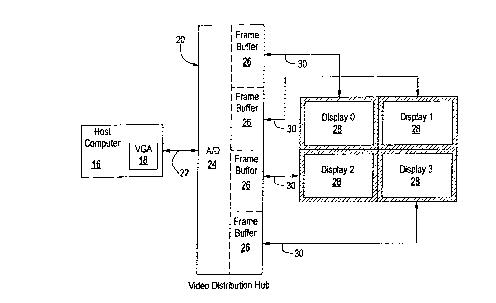
The present invention is illustrated from a macroscopic
point of view in Fig. 2. A host computer 16 provides input
data to a video graphics adapter (VGA) 18 via a host computer
ZO interface such as a PCI bus. The VGA 18 is typically a
circuit board installed within the host computer 16, though
other physical embodiments and placements are envisaged. The
graphics adapter 18 is used to generate text and graphical
video data from the input data, and to make such video data
available to display devices in an internal video display
buffer .
In the prior art, the digital video data in the video
display buffer is converted by the VGA 18 to an analog signal
comprised of components for each of the fundamental colors
employed by conventional display devices, red, green and blue
(RGB). This analog signal is then available for conveyance
to a conventional display device through a video data cable.
In the present invention, the video data in the video
display buffer is received by a video distribution hub 20 via
a video cable 22. Depending upon the protocol, horizontal
sync {HSYNC) and vertical sync (VSYNC) are derived locally
in the hub 20 from the analog RGB video data and/or through
additional sync signals conveyed through the video data cable
22, as discussed subsequently. The video cable 22 also
provides a DDC (display data channel) bus, a VESA (Video
Electronics Standards Association) standard bus, for the
purpose of enabling configuration control between the host
computer 16 and the hub 20. Additionally, in a further
embodiment, the video cable 22 provides a USB (Universal
Serial Bus) connection between the host computer 16 and the
hub 20, also for the purpose of configuration control. In
CA 02284176 1999-09-10
WO 98/41008 PCT/US98/04537
a first embodiment, however, the USB connections are for
future expansion and are terminated in a resistor pad found
in conjunction with frame buffer circuitry, discussed
subsequently.
The hub 20 is comprised of two major circuit blocks, an
analog-to-digital (A/D) front end 24, and plural frame
buffers 26. The A/D section 24 converts the color data for
each of the RGB colors into a digital representation, and
provides temporary storage for this digital data. There is
one frame buffer per color per associated display device 28,
or head; the frame buffers are each comprised of data gate
arrays (to be discussed subsequently) which enable the
storage of a selected portion of the video data coming from
the VGA 18 in a local memory. The selected portion then is
read out of the memory and is made available to the
respective head 28 through a frame buffer output interface
and associated cable 30.
The hub is an enclosure having approximate dimensions
of seven inches in width, one inch in height, and nine inches
in length, though other hub embodiments assume other relative
and absolute dimensions. Heat relief is provided as
required. Physical interfaces include an input port for
receiving the RGB video stream over the video cable 22 , a
power supply connection for interfacing to a +12V unregulated
(or regulated) power supply (not shown), and output ports for
each frame buffer 26 enabling interconnection of the display
device cable 30. LAN ports, such as a BNC connector and RJ45
connector, enabling intercommunication between plural hubs
are also provided in one embodiment. A serial port is also
provided, enabling a remote host (not necessarily the same
host as that which houses the respective video graphics
adapter) to provide command and control data to the hub, and
to return data. This serial link can be used, for instance,
to command the hub to initiate communication over the LAN
with other LAN-connected hubs. In an exemplary embodiment,
this serial port is an RS232 port.
CA 02284176 1999-09-10
WO 98/41008 PCT/US98/04537
_g_
In a preferred embodiment, the A/D section 24 and two
of the frame buffers 26 are disposed on a first circuit card
within the hub 20. Two further frame buffers 26 are located
on a separate circuit card, also within the hub 20. In
addition, in a further embodiment of the present invention,
up to eight frame buffers are supported within the hub, all
interfacing through a single A/D 24. Physical dimensions for
such a hub 20 would of course be adjusted to accommodate the
additional circuit cards.
The present invention is discussed at a more detailed
level with respect to Fig. 3. Here, the video display buffer
32, otherwise known as a large frame buffer, is illustrated
in association with the video graphics card 18. Again, the
RGB video data is illustrated as being conveyed from the
video graphics card 18 to the hub 20, and in particular to
the A/D section 24. Further detail on the A/D section is
presented below.
Between the A/D section 24 and the plural frame buffers
26 is an internal bus 34. As shown, this parallel bus is 48
bits wide; there are eight bits per pixel per each of the
three colors, or twenty-four bits per pixel, and it is
desired to transmit two pixels per clock cycle. Over this
bus 34 flows all of the digitized video data which
corresponds to the complete contents of the video display
large frame buffer 32 as received by the A/D section 24. It
is within the frame buffer 26 logic that the determination
of where to begin storing data and where to stop is made .
By starting and stopping the storage of video data, each
frame buffer section 26 is capable of providing to the
respective video head 28 only that portion 12 of the total
video display buffer 32 which is desired.
In Fig. 3, the frame buffers 26 are each illustrated as
being comprised of a logic section 36 and an SGRAM
(synchronous graphics RAM) 40. Essentially, the logic 36 is
responsible for storing in the SGRAM 40 only video data
associated with the video buffer portion 12 desired to be
CA 02284176 2004-02-27
-9-
displayed on the respective display device 28. The SGRAM 40 provides
temporary storage of this data to enable the timely provision of the data to
the
respective head 28. As will be discussed subsequently, there is logic and
SGRAM associated with each color for each of the display devices.
s
With respect to Figs. 4 and 11, the AID section 24 is described in detail.
An analog front end 42 AC couples the received analog RGB signal from the
video cable 22. After being coupled in, the video signal for each color is
approximately 0.7 Vpp, from the darkest to lightest extremes. Therefore, it is
Io necessary for the analog front end 42 to amplify the video signal for each
color,
thus improving the signal to noise ratio (SNR) of the following AID converters
(ADCs) 50. Suitable video preamps for this purpose include the National LM
1205 and LM 1283.
~s Gain control for these amplifiers (one per color) can be either fixed or
variable, depending upon the embodiment. Most simply, the gain control is
fixed by the factory. In a further variant, the gain control is fixed in the
factory,
though the user has physical access to a gain control adjusting means.
2o In another embodiment, the gain control is variable and is controlled by
a control circuit 44 in the AID section 24 having a digital to analog
converter
(DAC) for generation of the control signal. An appropriate D/A for this
purpose
is the Analog Devices AD8403AR10. The gain control (also referred to as
contrast control) is adjusted jointly for all three amplifiers (i.e. each of
RGB). In
2s addition, there are manual, independent balance adjustments for each of the
colors.
One A/D per color is employed in the embodiment of the present
invention. An alternative embodiment employs pixel interleaving due to the
3o compression afforded by this technique. Pixel interleaving is described in
commonly assigned U.S. Patent No. 5,742,274 entitled "Video Interface
System Utilizing Reduced Frequency Video Signal Processing". In a third
embodiment of the present invention not employing such interleaving, two
A/Ds per color are used for video rates above 75 MHz.
CA 02284176 2004-02-27
-1 ()
Since the analog input is AC coupled, it is necessary for the analog front
end 42 to also perform DC restore in order to establish a reference level in
the
amplified analog signal, for each of the colors. A back porch clamp is
employed for the purpose of clamping the amplified input signal to a known
s reference during a clamp interval, and is illustrated in Fig. 12. Other
clamping
or DC restore techniques can be employed.
In the preferred embodiment, eight bits per primary color are digitized. A
suitable device for the A/Ds 50 includes the Philips TDA8714. In an
alternative
embodiment, six bits are employed for color representation. The choice hinges
io upon desired (or required) color depth.
The eight-bit video data representations per color are clocked into two
banks of pixel bus buffers 54. One pixel's worth of data is clocked into one
bank of buffers 54 on even pixel clock cycles, while another pixel's worth of
is data is clocked into the other bank of buffers 54 on odd pixel clock
cycles.
Suitable buffers for this function include 74LVT574SM chips from Texas
Instruments.
Also in the A/D circuit block 24 is a sync processor 46, such as a
2o Mitsubishi M52347SP. There are three common video sync protocols. In the
first, each of HSYNC and VSYNC are provided separately as digital signals
between 1 - 5 Vpp. In the second, a composite digital sync signal is provided
on the HSYNC signal line. Lastly, an analog composite sync signal is extracted
from the green analog signal ("sync on green", or "SOG"), with a negative
2s polarity for positive video. Inputs to the sync signal processor 46
therefore
include externally received HSYNC and VSYNC, as well as the green analog
input signal. The sync processor 46 is configured to automatically select a
suitable one of these
...........................................................................
CA 02284176 1999-09-10
WO 98/41008
-11-
PCT/US98/04537
protocols.
Outputs of the sync processor include: HSYNC+ and
VSYNC+, correlating to HSYNC and VSYNC signal timings,
respectively; CLAMP+, used by the analog front end 42 in
timing the DC restore, as previously discussed; and status
bits usable by local processing to indicate what sync type
was input to the sync processor 46.
HSYNC+ is used as an input to a phase fine tune (PFT)
circuit 48. The PFT 48 adjusts where the video signal is
sampled by the ADC 50 within a pixel lifetime by employing
an adjustable delay of HSYNC+. The output of an RC charging
circuit such as that shown in Fig. 14 is compared, using for
instance an Analog Devices AD9696, with a control voltage
generated by the control circuit 44 in the generation of
H(pft)+. An external adjustment such as an encoder is
provided on the exterior of the hub 20 chassis to enable
manual adjustment of the control voltage, in an illustrative
embodiment. Other encoders exist, such as those on the
attached heads 28. The state of these encoders is also
reported back to the control circuit 44. Therefore, the
present invention is responsive to adjustment of PFT at
either a central location such as the hub, or remotely, such
as at the heads.
Also within the A/D circuit block 24 is a video clock
regenerator circuit 52 including a fully programmable clock
regenerator such as an ICS1522 made by Integrated Circuit
Systems, Inc., a phase locked loop (PLL) frequency
synthesizer. The clock regenerator is serially programmed
in a preferred embodiment of the present invention by the
control circuit 44 to generate four clock outputs, each at
1/4 the sampled pixel rate and 90 degrees out of phase with
the following output, which collectively comprise a clock at
the sampled pixel rate. Various frequencies are employed,
depending upon the video data rate. For illustrative
purposes, 75 MHz is used herein.
In addition to the clock regenerator/frequency
CA 02284176 1999-09-10
WO 98/41008 PCT/US98/04537
-12-
synthesizer, the clock regenerator circuit 52 is comprised
of a MOSFET bus switch, such as a Texas Instruments 74CBT3125
quad bus switch. The purpose of the MOSFET bus switch is to
generate two 75/2 MHz clocks, 180 degrees out of phase with
each other, from the four 75/4 MHz staggered clock signals
from the clock regenerator/frequency synthesizer.
With respect to Fig. 15, four switches are provided in
the 74CBT3125 bus switch used in the preferred embodiment.
Each switch is a MOSFET switch having an inverted-input
output-enable associated therewith. The first clock signal
from the clock regenerator is fed to the input of the first
switch, and the second clock signal, 90 degrees out of phase
{lagging) with the first clock signal, is connected to the
output enable for the first switch. The third and fourth
clock signals are connected to the second switch in a similar
manner. The outputs of the first two switches are then tied
together, providing an output clock with clean rising edges
due to the speed of the switches and having a period of 75/2
MHz.
Likewise, clock two is connected to the input of switch
three, and clock three is connected to the output enable of
switch three. Clock four is connected to the input of switch
four, and clock one is connected to the output enable of
switch four. The outputs of switches three and four are also
tied together. The resulting output is also a 75/2 MHz clock
signal, though 180 degrees out of phase with the output from
the first two switches.
Each of the 75/2 MHz outputs from the bus switch are
used to clock a respective PLL clock driver such as the
CDC536 from Texas Instruments as part of the video clock
regenerator 52. This part enables the generation of a
doubled output, a 75 MHz clock also referred to as the ADCLK
or "dot clock", which is used to clock the ADCs 50. Once
again, other frequencies are employable as required.
In addition, the clock driver provides 75/2 MHz clocks
("PCLK/2+" and "PCLK/2-") of like phase with respect to the
CA 02284176 1999-09-10
WO 98/41008
PCT/US98/04537
-13-
clocks from which they are derived. Such clocks are used to
clock the pixel bus buffers 54 latching digital video data
out of the ADCs 50, since data gate arrays in the frame
buffer logic 36 can't run at speeds such as 75 MHz (data gate
arrays are discussed later).
In the first embodiment of the present invention, the
sampling rate does not exceed 75 MHz, with the limitation
being found in the analog preamplifier of the analog front
end 42 and in the speed of the ADCs 50.
The clock regenerator circuit 52 also enables the
regeneration of HSYNC, in a form referred to as LOCHSYNC, or
local HSYNC, even without an external HSYNC. Thus, an on-
screen display chip is utilized in a further embodiment of
the present invention for the generation of on-screen menus.
LOCHSYNC is employed by the control circuit 44 in controlling
the output of the frame buffers 26.
The on-screen display chip (not illustrated) is employed
in the A/D circuit block 24, and specifically, in conjunction
with the analog front end 42. Analog output from this chip
is mixed into the A/Ds 50. A single user interface to this
chip is provided.
In one embodiment of the present invention, control over
when and for what duration a frame buffer 26 captures video
data resides within the A/D circuit block 24, and in
particular within the video clock regenerator 52 using gating
signals. However, since such signals would only gate one
frame buffer 26, such embodiment is not preferred.
The control circuit 44 provides a VSYNC disable to the
3o video clock regenerator 52 to disable the PLL during vertical
intervals. Otherwise, spikes generated by the PLL in the
vertical interval would cause errors in forward error
correction.
Functions of the control circuit 44 in the A/D circuit
block 24 have previously been alluded to, such as the
generation of the analog preamplifier gain control, creation
of VControl for use in the PFT 48, generation of the Vsync
CA 02284176 1999-09-10
WO 98/41008 PCT/US98/04537
-14-
disable and serial data signals for use in the video clock
regenerator 52. Structurally, the control circuit comprises
in a preferred embodiment the following elements.
As discussed, a DAC is required in the generation of
amplifier gain control. Other elements comprising the
control circuit include a serially programmable digital
potentiometer, such as an Analog Devices AD8403AR10, which
enables the generation of A/D circuit-internal control
signals such as: CONTRAST, an adjustment to the video preamp
in the analog front end 42; CLAMP WDTH, used in the sync
signal processor; and the PFT control signal previously
discussed.
Primarily, however, the control circuit is comprised of
a C25 microprocessor with an XC5202 microprocessor gate
array. Principal signals received by the control circuit 44
include clocks from the video clock regenerator 52, and
HSYNC+ and VSYNC+ from the sync processor 46. Clearly, in
the actual implementation, there is a much higher degree of
interconnectivity than that which is alluded to here.
For the purposes of programming the control circuit 44,
a serial PROM and a parallel EEPROM provide data to the gate
array and microprocessor, respectively. The use of the
parallel EEPROM enables the reprogrammability of the hub.
Further, the microprocessor and associated gate array are in
communication with devices external to the hub 20 via a
serial port disposed on one end of the hub 20. A UART
(universal asynchronous receiver/transmitter), such as a
TL16C550A, and a TTL to EIA level translator such as an
MAX211E, enable this serial communication.
The control circuit is also in communication with
devices external to the hub 20 through LAN ports, such as BNC
or RJ45 connectors. Standard LAN interfaces are employed in
a preferred embodiment, such as an SMC91C94 LAN chip, coupled
to a DP8392 encoder. Such a LAN interface enables
programmability of the hub 20 as an addressable port on a LAN
shared by devices other than hubs, or as a port on a LAN
CA 02284176 1999-09-10
WO 98/41008
PCT/US98/04537
-15-
dedicated solely to one or more hubs in communication with
a configuring device or devices. In either case, the hub 20
is a "dumb" device which only responds when directed to from
an intelligent device. The serial communication can be
either lOBase2 or lOBaseT.
Finally, as previously noted, a DDC bus enables
configuration of the hub 20 by the host computer 16. This
bus is comprised of twa data signals, SDA (serial data) and
SCL (serial clock), +5 VDC, and return. The DDC channel is
normally employed, in the prior art, as a unidirectional
pathway to a repository of peripheral device configuration
information available to a host. Here, however, the C25
processor reads and writes the DDC memory dynamically with
information pertaining to the configuration of the hub and
the attached heads. The DDC memory, which can be discrete
or part of the control circuit memory, is then read by a
host.
Therefore, the control circuit can be configured, or
reconfigured, via internal replacement of programmed memory
devices, external communication to removable configuring
devices such as via a LAN interface, or by input from the
host computer. Such configuration information can include,
explicitly or implicitly, the point (row and pixel) within
the frame at which each displayed segment is to begin.
From the A/D circuit block 24, digital video data is
provided in parallel as eight bits per color per pixel, with
two pixels being provided per clock cycle, for a total of 48
bits. Other signals which are provided by the A/D circuit
block 24 include : USB signals, which are for future expansion
in the present embodiment and are therefore terminated at a
' daughter board connector proximate the frame buffer
circuitry; horizontal and vertical sync signals from the sync
signal processor 46; various clock signals originating in the
video clock regenerator 52; a start of frame signal generated
by the control circuit 44 from the horizontal and vertical
syncs; and serial control data also generated by the control
CA 02284176 1999-09-10
WO 98/41008 PCT/US98/04537
-16-
circuit 44.
One frame buffer circuit block 26 is illustrated in Fig.
at a first order of detail, bearing in mind that there are
up to four frame buffer circuit blocks 26 in each hub in a
5 first embodiment, each capable of providing digital video
data to a respective display head 28.
Sixteen parallel bits of video data per color (two
pixels) are received by a respective data gate array 56. The
data gate array 56 enables the storage of the video data in
the respective SGRAM 40 if the data is part of the desired
portion 12 of the video display buffer in the VGA 18, based
upon control received from an associated control gate array
58. In the preferred embodiment of the present invention,
there is one control gate array 58 per frame buffer logic
circuit 36, though in an alternative embodiment, one control
gate array 58 is shared between two frame buffer logic
circuits 36.
If the video data is desired for display on the
associated head 28, the data is stored in the respective,
single-ported SGRAM 40. As required, the data is then
removed from the SGRAM 40 where it passes again through the
data gate array 56 to the panel link 60, the latter acting
as an output interface to the associated head 28.
On a more detailed level, Fig. 6 provides an
illustration of a data gate array 56 and an associated SGRAM
40 for a single color channel. Video data input to the data
gate array 56 for one of the three colors, two parallel
eight-bit pixels, is received on sixteen parallel signal
paths at approximately 80 MPixels/sec (or 40 MPixelPairs/sec)
within a demux 63 in the data gate array 56. This demux 63
enables the distribution of the input data into two sixteen
bit registers 64, which in turn provide thirty-two bit
parallel data to a 32 bit wide, 16 bit deep write FIFO 66.
How the data is transferred into the registers 64
depends upon the type of head 28 associated with this color
channel as conveyed by the head 28 to the control circuit 44
CA 02284176 1999-09-10
WO 98/41008 PCT/US98/04537
-17-
(via the DDC backchannel) through the serial port to the
control gate array 58 (on a separate serial bus) . For an
active matrix LCD display, all eight bits per pixel are
utilized. As shown in Figs. 7 and 9, the upper of the two
registers 64 is filled with four four-bit nibbles during
clock cycle zera, representing two eight-bit pixels for this
color. On clock cycle one, two more pixels are loaded into
the lower sixteen-bit register 64. On the following clock
cycle, clock cycle two, the 32 bits of data representing four
pixels for this color are clocked into the write FIFO 66 and
the upper register 64 is written with the next two pixels.
The clock speed into the write FIFO 66 is 20 MHz for active
matrix displays in the first embodiment of the present
invention. Other exemplary embodiments employ other clock
speeds.
If the associated head 28 is a passive matrix display,
the lower four bits of each eight bit pixel are dropped and
the upper four bits are clocked into the registers 64 as
indicated in Figs. 8 and 10. On successive clock cycles, the
upper four bits for each pixel are stored in respective
portions of the registers 64, while the lower four bits are
dropped. On clock cycle four, the data in the registers 64
are clocked out to the write FIFO 66 and the process of
receiving the upper four bits per pixel in the registers 64
begins again. The clock speed into the write FIFO 66 for
passive matrix displays is 10 MHz.
The output of the write FIFO 66 is connected to a 32-bit
data path. Also connected to this data path are the
respective single-ported SGRAM 40, which is 32 bits wide by
256 kbytes deep, and a read FIFO 68 of the same dimensions
as the write FIFO 66. A suitable SGRAM 40 for this
application is an IBM038329N06A-10, which operates at 50 MHz.
Desired video buffer portion 12 data from the write FIFO 66
is read into the SGRAM 40 under the control of the control
gate array 58.
In a first embodiment of the present invention, data out
CA 02284176 1999-09-10
WO 98/41008 PCT/US98/04537
-18-
of the write FIFO 66 is written to the SGRAM 40 for eight
clock cycles, the 32-bit wide bus is idle for two clock
cycles, data is read out of the SGRAM 40 and into the read
FIFO 68 for eight clock cycles, then the bus goes idle for
another two clock cycles. The desired portion 12 data can
be any contiguous portion of the video buffer data from the
video graphics adapter 18 in the host computer 16, limited
maximally in size by the characteristics of the associated
head 28.
When and how much data is stored in the SGRAM 40 is
mandated by the control gate array 58. In a first, preferred
embodiment of the present invention, the control circuit 44
in the A/D circuit block 24 provides the control gate array
58 in the frame buffer logic block 26 with horizontal and
vertical offsets, relative to the start of frame
notification, via the serial data path between the two for
the commencement of data storage in the SGRAM 40. These
offsets are used to control a video microsequencer
implemented in the control gate array 58 for enabling the
transfer of digital video data into the video registers 64,
and subsequently into the write FIFO 66. A memory
controller, also implemented in the control gate array 58,
controls the transfer of data from the write FIFO 66 to the
SGRAM 40, and from the SGRAM 40 to the read FIFO 68.
Finally, a panel microsequencer, again, implemented in the
control gate array 58, controls the output of data from the
read FIFO 68 to Frame Rate Modulation (FRM} logic 70
(discussed subsequently}.
The benefit of providing these three independent
elements, the video microsequencer, the memory controller,
and the panel sequencer, lies in that the writing of data can
take place at a different rate than the reading of data; the
memory controller effectively disconnects the potentially
disparate write and read function rates.
The programming of the video microsequencer with the
offset information is preferred due to the ease of adjusting
CA 02284176 1999-09-10
WO 98/41008
PCTNS98/04537
_19_
the offset values when a respective head is replaced or when
the display characteristics for a head are changed. How much
data to store is calculated by the control circuit 44 based
upon display size, resolution, and orientation as learned
from the respective head 28 via the DDC backchannel. The
frame signal is used for interlaced video applications, the
control gate array 58 using this signal to identify even
versus odd frames.
In alternative embodiments, data storage in the SGRAM
40 is solely under the control of the control circuit 44,
the latter sending the equivalent of "on" and "off" signals
to the control gate array 58. A drawback of such control
lies in the need for separate control lines between the
control circuit 44 and each control gate array 58.
In yet another embodiment, the control circuit 44
provides "on" signals to the control gate array 58, and the
control gate array 58 provides the "off" signal based upon
backchannel information relating to the associated head 28.
The multiplicity of control signals is once again a drawback
of this embodiment.
The memory controller tracks the data flowing into and
out of the FIFOs 66, 68 and the SGRAM 40. If the write FIFO
66 is less than half full, a write to the SGRAM 40 from the
write FTFO 66 is disabled; if the read FIFO 68 is more than
half full, the SGRAM 40 is prevented from writing to the read
FIFO 68. The bus intermediate the FIFOs 66, 68 and the SGRAM
40 remains idle during the clock cycles which would otherwise
be used for writing data from or reading data to the SGRAM
40.
From the read FIFO 68, data is clocked into a frame rate
modulation logic circuit (FRM) 70 which formats the 32-bit
wide data according to whether the associated head 28 is
passive or active matrix, and outputs eight-bit wide data to~
the panel link 60 associated with that frame buffer 26 (there
is one panel link 60 per frame buffer 26) . For active matrix
displays, the FRM 70 executes an algorithm which reserializes
CA 02284176 1999-09-10
WO 98/41008 PCT/US98/04537
-20-
the input data by taking the four, eight-bit wide pixels,
buffering them, and outputting the data as sequential eight
bit wide pixel data. The maximum input rate into the panel
link from the FRM 70 is up to 65 MHz in the present
embodiment.
For a passive matrix array as the associated head 28,
the FRM 70 executes a conversion algorithm which also
receives 32 parallel bits, but in the form of eight, four-bit
pixels . The algorithm converts the four bit pixels into one-
bit pixels using frame rate modulation. This involves the
use of a look-up table in the FRM 70 and the frame number
which is passed from the A/D control circuit 44 to the
control gate array 58 to the FRM 70. The algorithm
effectively averages the color of the same pixel over time,
and compares the possible values for this pixel against that
of surrounding pixels to enable the use of one-bit per pixel
with minimized visual artifacts. The output of the FRM 70
for an associated passive matrix display is eight parallel
one-bit pixels. Alternatively, any suitable FRM technique
may be employed.
In an alternative embodiment in which the speed of the
SGRAM 40 is sufficiently greater than that currently
available, the data format for an associated passive matrix
display could be four eight-bit pixels in parallel into the
FRM 70, instead of the current eight four-bit pixels.
In a passive matrix display, the frame rate is twice
that of the active matrix display. Typical values are 120
Hz frame rate for a passive matrix display versus 60 Hz for
an active matrix display. The chief advantage of passive
matrix displays is cost; presently, such passive displays
cost roughly one-third the cost of active matrix displays.
An active matrix display may take two pixels per clock
cycle, in order. However, a "dual scan passive" display
provides four one-bit pixels per clock cycle at both a top
and bottom half of a display. Thus the difference in frame
rate.
CA 02284176 1999-09-10
WO 98/41008 PCT/US98/04537
-21-
The panel link 60 receives eight bits per pixel per
color, or 24 bits per pixel total, at up to 65 MHz for an
associated active matrix panel head 28, four times the FRM
70 input clock rate. The panel link 60 receives pixel data
for an associated passive matrix display at approximately 20
MHz, the same as the input rate into the FRM 70.
The panel link 60, such as a Chips & Technologies 65100,
formats the input data for provision to the respective head
28. It receives the three eight-bit data streams from the
FRMs 70, one for each color, and using the HSYNC and VSYNC
signals from the A/D control circuit 44 via the control gate
array 58 formats the data for output over four differential
lines at a connector to the respective head 28.
The panel link provides its outputs to the respective
head 28 over the display device cable 30 as four twisted
pairs. This cable 30 also provides 12V power and ground, a
USB backchannel (the latter not being employed in the present
embodiment), and the DDC backchannel to the control circuit
40. Four of the twisted pairs are for the RGB data and data
clock. One twisted pair is for the DDC backchannel. Another
twisted pair is for the USB. Each of the USB and DDC
backchannels provide individual data and clock paths, and
share 5V, 12V and ground which are also conveyed in this
cable to the respective head 28.
Other elements of the presently disclosed hub 20 include
registers which preserve the setup information of the panel
link 60, data gate array 56, and other elements, as received
from the control circuit 44.
The power requirements for the present hub 20 are
.30 unregulated 12 VDC. This is supplied to DC/DC converters
which generate 5V and 3.3V for use as logic supplies. The
unregulated 12 VDC is used as an input to an analog power and
control circuit which includes a switching DC/DC converter
72 , as shown in Fig . 16 . The 12 VDC is appl ied to a buck
switching regulator drive 74. This drive can take many
forms, such as a switching regulator (e. g. a Linear
CA 02284176 1999-09-10
WO 98/41008 PCT/US98104537
-22-
Technology LT1376), or a regulator controller. The output
of this drive 74, essentially a 12 Vpp rectangular wave, is
coupled through an inductor 80 to a filter capacitor (or
capacitors) 82 at the output of the inductor 80 in the common
buck configuration, to supply 5 VDC for use in the analog
section.
The output of the regulator drive 74 is also employed
to drive a charge pump providing a higher-voltage input to
an auxiliary DC supply circuit, generally designated 84 in
Fig. 16. This circuit 84 includes alternately-conducting
diodes 86, and one or more reservoir capacitors 88 coupled
to a micropower low dropout regulator (e. g. a Linear
Technology LT1129} 90, effectively providing a regulated,
auxiliary 12 VDC output. Other voltages can be generated,
depending upon system requirements.
In an alternative embodiment of the present invention,
the hub 20 is configured to accept a digital video input.
The data gate array 56 in this embodiment is configured to
properly format the input digital data prior to its
processing by the write FIFO 66, the SGRAM 40, the read FIFO
68, the FRM 70, and the panel link 60. Such a hub 20 can be
configured to accept either analog data input as previously
described or digital data input, or can accept just digital
data, eliminating some of the cost of the circuitry
associated with the analog front end in the A/D circuit block
24. In an embodiment of the present hub 20 which accepts
digital data directly, buffers such as the pixel bus buffers
54 are employed to temporarily hold the digital data prior
to processing by the data gate array 56.
In yet further alternative embodiments, the digital
output of the hub is employed as a digital input to one or
more subsequent hubs. The panel link interface 60 can also
be replaced with D/A converters. Such an embodiment could
then drive conventional CRTs, or could provide analog input
to one or more subsequent hubs. Additionally, the inputs and
outputs of the hub 20 can be adapted to receive and/or
CA 02284176 1999-09-10
WO 98/41008 PCT/US98/04537
-23 -
transmit data in an optical format.
Modifications and substitutions to the present invention
made by one of ordinary skill in the art is considered to be
within the scope of the present invention, which is not to
be limited except by the claims which follow.