Note: Descriptions are shown in the official language in which they were submitted.
CA 02284542 1999-09-20
WO 98/44385 PCT/US98/05989
ELECTROCHROMIC REARVIEW MIRROR
INCORPORATING A THIRD SURFACE METAL
REFLECTOR
BACKGROUND OF THE INVENTION
This invention relates to electrochromic rearview mirrors for motor vehicles
and, more particularly, to improved electrochromic rearview mirrors
incorporating third
surface reflector/electrode in contact with at least one solution-phase
electrochromic
material.
Heretofore, various rearview mirrors for motor vehicles have been proposed
which change from the full reflectance mode (day) to the partial reflectance
mode(s)
(night) for glare-protection purposes from light emanating from the headlights
of
vehicles approaching from the rear. Among such devices are those wherein the
transmittance is varied by thermochromic, photochromic, or electro-optic
(e.g., liquid
crystal, dipolar suspension, electrophoretic, electrochromic, etc.) means and
where the
variable transmittance characteristic affects electromagnetic radiation that
is at least
partly in the visible spectrum (wavelengths from about 3800A to about 7800A).
Devices of reversibly variable transmittance to electromagnetic radiation have
been
proposed as the variable transmittance element in variable transmittance light-
filters,
variable reflectance mirrors, and display devices which employ such light-
filters or
mirrors in conveying information. These variable transmittance light filters
have
included windows.
Devices of reversibly variable transmittance to electromagnetic radiation,
wherein the transmittance is altered by electrochromic means, are described,
for
example, by Chang, "Electrochromic and Electrochemichromic Materials and
Phenomena," in Non-emissive Electroo tip c Displays, A. Kmetz and K. von
Willisen,
eds. Plenum Press, New York, NY 1976, pp. 155-196 (1976) and in various parts
of
Eletrochromism, P.M.S. Monk, R.J. Mortimer, D.R. Rosseinsky, VCH Publishers,
Inc.,
New York, NY (1995). Numerous electrochromic devices are known in the art.
See,
e.g., Manos, U.S. Pat. No. 3,451,741; Bredfeldt et al., U.S. Pat. No.
4,090,358; Clecak
et al., U.S. Pat. No. 4,139,276; Kissa et al., U.S. Pat. No. 3,453,038;
Rogers, U.S. Pat.
1
SUBSTITUTE SHEET (RULE 26)
CA 02284542 2004-10-29
Nos. 3,652,149, 3,774,988 and 3,873,185; and Jones et al., U.S. Patent Nos.
3,282,157,
3,282,158, 3,282,160 and 3,283,656.
In addition to these devices there are commercially available electrochromic
devices and associated circuitry, such as those disclosed in U.S. Patent No.
4,902,108,
entitled "Single-Compartment, Self-Erasing, Solution-Phase Electrochromic
Devices
Solutions for Use Therein, and Uses Thereof', issued Feb. 20, 1990 to H. J.
Byker;
Canadian Patent No. 1,300,945, entitled "Automatic Rearview Mirror System for
Automotive Vehicles", issued May 19, 1992 to J. H. Bechtel et al.; U.S. Patent
No.
5,128,799, entitled "Variable Reflectance Motor Vehicle Mirror", issued Jul.
7, 1992 to
H. J. Byker; U.S. Patent No. 5,202,787, entitled "Electro-Optic Device",
issued Apr. 13,
1993 to H. J. Byker et al.; U.S. Patent No. 5,204,778, entitled "Control
System For
Automatic Rearview Mirrors", issued Apr. 20, 1993 to J. H. Bechtel; U.S.
Patent No.
5,278,693, entitled "Tinted Solution-Phase Electrochromic Mirrors", issued
Jan. 11,
1994 to D. A. Theiste et al.; U.S. Patent No. 5,280,380, entitled "UV-
Stabilized
Compositions and Methods", issued Jan. 18, 1994 to H. J. Byker; U.S. Patent
No.
5,282,077, entitled "Variable Reflectance Mirror", issued Jan. 25, 1994 to H.
J. Byker;
U.S. Patent No. 5,294,376, entitled "Bipyridinium Salt Solutions", issued Mar.
15, 1994
to H. J. Byker; U.S. Patent No. 5,336,448, entitled "Electrochromic Devices
with
Bipyridinium Salt Solutions", issued Aug. 9, 1994 to H. J. Byker; U.S. Patent
No.
5,434,407, entitled "Automatic Rearview Mirror Incorporating Light Pipe",
issued Jan.
18, 1995 to F. T. Bauer et al.; U.S. Patent No. 5,448,397, entitled "Outside
Automatic
Rearview Mirror for Automotive Vehicles", issued Sep. 5, 1995 to W. L. Tonar;
and
U.S. Patent No. 5,451,822, entitled "Electronic Control System", issued Sep.
19, 1995
to J. H. Bechtel et al. Each of these patents is commonly assigned with the
present
invention. Such electrochromic devices may be utilized in a fully integrated
inside/outside rearview mirror system or as separate inside or outside
rearview mirror
systems.
Figure 1 shows a typical electrochromic mirror device 10, having front and
rear
planar elements 12 and 16, respectively. A transparent conductive coating 14
is placed
on the rear face of the front element 12, and another transparent conductive
coating 18
is placed on the front face of rear element 16. A reflector (20a, 20b and
20c), typically
2
CA 02284542 1999-09-20
WO 98/44385 PCT/US98/05989
comprising a silver metal layer 20a covered by a protective copper metal layer
20b, and
one or more layers of protective paint 20c, is disposed on the rear face of
the rear
element 16. For clarity of description of such a structure, the front surface
of the front
glass element is sometimes referred to as the first surface, and the inside
surface of the
front glass element is sometimes referred to as the second surface. The inside
surface
of the rear glass element is sometimes referred to as the third surface, and
the back
surface of the rear glass element is sometimes referred to as the fourth
surface. The
front and rear elements are held in a parallel and spaced-apart relationship
by seal 22,
thereby creating a chamber 26. The electrochromic medium 24 is contained in
space
1o 26. The electrochromic medium 24 is in direct contact with transparent
electrode layers
14 and 18, through which passes electromagnetic radiation whose intensity is
reversibly
modulated in the device by a variable voltage or potential applied to
electrode layers 14
and 18 through clip contacts and an electronic circuit (not shown).
The electrochromic medium 24 placed in space 26 may include surface-
confined, electrodeposition type or solution-phase type electrochromic
materials and
combinations thereof. In an all solution-phase medium, the electrochemical
properties
of the solvent, optional inert electrolyte, anodic materials, cathodic
materials, and any
other components that might be present in the solution are preferably such
that no
significant electrochemical or other changes occur at a potential difference
which
oxidizes anodic material and reduces the cathodic material other than the
electrochemical oxidation of the anodic material, electrochemical reduction of
the
cathodic material and the self-erasing reaction between the oxidized form of
the anodic
material and the reduced form of the cathodic material.
In most cases, when there is no electrical potential difference between
transparent conductors 14 and 18, the electrochromic medium 24 in space 26 is
essentially colorless or nearly colorless, and incoming light (Io) enters
through front
element 12, passes through transparent coating 14, electrochromic containing
chamber
26, transparent coating 18, rear element 16 and reflects off layer 20a and
travels back
through the device and out front element 12. Typically, the magnitude of the
reflected
image (IR) with no electrical potential difference is about 45 percent to
about 85 percent
of the incident light intensity (Io). The exact value depends on many
variables outlined
below, such as, for example, the residual reflection (I'R) from the front face
of the
3
SUBSTITUTE SHEET (RULE 26)
= CA 02284542 1999-09-20
WO 98/44385 PCT/US98/05989
front element, as well as secondary reflections from the interfaces between:
the front
element 12 and the front transparent electrode 14; the front transparent
electrode 14 and
the electrochromic medium 24; the electrochromic medium 24 and the second
transparent electrode 18; and the second transparent electrode 18 and the rear
element
16. These reflections are well known in the art and are due to the difference
in
refractive indices between one material and another as the light crosses the
interface
between the two. If the front element and the back element are not parallel,
then the
residual reflectance (I'R) or other secondary reflections will not superimpose
with the
reflected image (I,) from mirror surface 20a, and a double image will appear
(where an
1o observer would see what appears to be double (or triple) the number of
objects actually
present in the reflected image).
There are minimum requirements for the magnitude of the reflected image
depending in whether the electrochromic mirrors are placed on the inside or
the outside
of the vehicle. For example, according to current requirements from most
automobile
manufacturers, inside mirrors must have a high end reflectivity of at least 70
percent
and outside mirrors must have a high end reflectivity of at least 50 percent.
Electrode layers 14 and 18 are connected to electronic circuitry which is
effective to electrically energize the electrochromic medium, such that when a
potential
is applied across the transparent conductors 14 and 18, electrochromic medium
in space
26 darkens such that incident light (Io) is attenuated as the light passes
toward the
reflector 20a and as it passes back through after being reflected. By
adjusting the
potential difference between the transparent electrodes, such a device can
function as a
"gray-scale" device, with continuously variable transmittance over a wide
range. For
solution-phase electrochromic systems, when the potential between the
electrodes is
removed or returned to zero, the device spontaneously returns to the same,
zero-
potential, equilibrium color and transmittance as the device had before the
potential was
applied. Other electrochromic materials are available for making
electrochromic
devices. For example, the electrochromic medium may include electrochromic
materials that are solid metal oxides, redox active polymers and hybrid
combinations of
solution-phase and solid metal oxides or redox active polymers; however, the
above-
described solution-phase design is typical of most of the electrochromic
devices
4
SUBSTITUTE SHEET (RULE 26) ----
CA 02284542 1999-09-20
WO 98/44385 PCT/US98/05989
presently in use.
Even before a fourth surface reflector electrochromic mirror was commercially
available, various groups researching electrochromic devices had discussed
moving the
reflector from the fourth surface to the third surface. Such a design has
advantages in
that it should, theoretically, be easier to manufacture because there are
fewer layers to
build into a device, i.e., the third surface transparent electrode is not
necessary when
there is a third surface reflector/electrode. Although this concept was
described as early
as 1966, no group had commercial success because of the exacting criteria
demanded
from a workable auto-dimming mirror incorporating a third surface reflector.
U.S.
lo Patent No. 3,280,701, entitled "Optically Variable One-Way Mirror", issued
Oct. 25,
1966 to J. F. Donnelly et al has one of the earliest discussions of a third
surface
reflector for a system using a pH-induced color change to attenuate light.
U.S. Patent No. 5,066,112, entitled "Perimeter Coated, Electro-Optic Mirror",
issued Nov. 19, 1991, to N. R. Lynam et al., teaches an electro-optic mirror
with a
conductive coating applied to the perimeter of the front and rear glass
elements for
concealing the seal. Although a third surface reflector is discussed therein,
the
materials listed as being useful as a third surface reflector suffer from one
or more of
the following deficiencies: not having sufficient reflectivity for use as an
inside mirror,
or not being stable when in contact with a solution-phase electrochromic
medium
containing at least one solution-phase electrochromic material.
Others have broached the topic of a reflector/electrode disposed in the middle
of
an all solid state-type devices. For example U.S. Patent Nos. 4,762,401;
4,973,141; and
5,069,535 to Baucke et al. teach an electrochromic mirror having the following
structure: a glass element; a transparent (ITO) electrode; a tungsten oxide
electrochromic layer; a solid ion-conducting layer; a single layer hydrogen
ion-
permeable reflector; a solid ion conducting layer; a hydrogen ion storage
layer; a
catalytic layer; a rear metallic layer; and a back element (representing the
conventional
third and fourth surface). The reflector is not deposited on the third surface
and is not
directly in contact with electrochromic materials, certainly not at least one
solution-
phase electrochromic material and associated medium.
Consequently, it is desirable to provide an improved high reflectivity
5
SUBSTITUTE SHEET (RULE 26)
~ CA 02284542 1999-09-20
WO 98/44385 PCT/US98/05989
electrochromic rearview mirror having a third surface reflector/electrode in
contact a
solution-phase electrochromic medium containing at least one electrochromic
material .
OBJECTS OF THE INVENTION
Accordingly, a primary object of the present invention is to provide an
improved, robust, low cost dimmable rearview mirror incorporating a high
reflectivity
third surface reflector/electrode for motor vehicles, which mirror is capable
of
operating in harsh environments over wide variations in temperature, humidity,
vibration, atmospheric corrosion, salt spray, electronic disturbances, and
sand and grit,
and which is relatively economical and reliable to consistently manufacture
and
assemble, and is durable, efficient and reliable in operation.
Another object of the present invention is to provide an improved dimmable
rearview mirror for motor vehicles wherein excellent speed of reflectance
change,
excellent high end reflectance, good uniformity of reflectance change across
the
surface area of the mirror, neutral color or appearance in the high
reflectance state,
continually variable reflectance and good low end reflectance are obtained.
Another object of the present invention is to provide improved high
conductance contact or buss bars for the second surface transparent conductive
electrode by using a portion of the third surface reflector/electrode and a
conductive
seal or strip to make electrical contact to the transparent conductive
electrode on the
second surface.
SUMMARY OF THE INVENTION
The above and other objects, which will become apparent from the
specification as a whole, including the drawings, are accomplished in
accordance with
the present invention by incorporating a reflector/electrode on the inside
(third)
surface of a dimming portion of the rearview mirror. This reflector/electrode
forms an
integral electrode in contact with at least one solution-phase electrochromic
material,
and may be a single layer of a highly reflective silver alloy or may comprise
a series
of coatings where the outer coating is a highly reflective silver alloy. When
a series of
coatings is used for the reflector/electrode, there should be a base coating
which bonds
to the glass surface and resists any adverse interaction, e.g., corrosive
action, with any
6
SUBSTITUTE SHEET (RULE 26)
. . _ T...._.__ ~..--
CA 02284542 1999-09-20
WO 98/44385 PCT/US98/05989
constituents of the electrochromic medium, an optional intermediate layer (or
layers)
which bonds well to the base coating and resists any adverse interaction with
the
electrochromic medium, and at least one highly reflective silver alloy which
directly
contacts the electrochromic medium and which is chosen primarily for its
adequate
bond to the peripheral seal, its high reflectance, good shelf life, stable
behavior as an
electrode, resistance to adverse interaction with the electrochromic medium,
resistance
to atmospheric corrosion, resistance to electrical contact corrosion, the
ability to
adhere to the base or intermediate layer(s), if present. If a single layer of
highly
reflective silver alloy is utilized, it must also meet these operational
criteria.
In another embodiment of the present invention, when a very thin over-coating
is placed over the highly reflective layer, then the highly reflective layer
may be silver
metal or a silver alloy.
In yet another embodiment of the present invention, the third surface
reflector/electrode includes at least one base layer that is disposed over the
entire third
surface of the electrochromic mirror. A highly reflective layer is disposed
over the
central portion of the base layer(s) and not over the perimeter edge portion
where the
seal will be placed. Optionally, one or more intermediate layers may be
disposed
between the base and reflective layers, and may be placed over the entire
third surface
or may be placed over the central portion or both (if there is more than one
intermediate layer).
The third surface reflector of the present invention may additionally provide
for significant improvement of the electrical interconnection techniques used
to impart
a voltage or drive potential to the transparent conductor on the second
surface of the
electrochromic mirror. This is accomplished both by providing improved contact
stability between the contacts, such as clips, and the reflector layer and by
providing
unique and advantageous buss bar configurations.
BRIEF DESCRIPTION OF THE DRAWINGS
The subject matter which is regarded as the invention is particularly pointed
out and distinctly claimed in the concluding portion of the specification. The
invention, together with further objects and advantages thereof, may best be
understood by reference to the following description taken in connection with
the
7
SUBSTITUTE SHEET (RULE 26)
~ CA 02284542 1999-09-20
WO 98/44385 PCT/US98/05989
accompanying drawings, where like numerals represent like components, in
which:
FIG. 1 is an enlarged cross-sectional view of a prior art electrochromic
mirror assembly;
FIG. 2 is a front elevational view schematically illustrating an
inside/outside electrochromic rearview mirror system for motor vehicles where
the
inside and outside mirrors incorporate the mirror assembly of the present
invention;
FIG. 3 is an enlarged cross-sectional view of the inside electrochromic
rearview mirror incorporating a third surface reflector/electrode illustrated
in FIG.
2, taken on the line 2-2' thereof;
FIG. 4 is an enlarged cross-sectional view of an electrochromic mirror
incorporating an alternate embodiment of a third surface reflector/electrode
according to the present invention;
FIG. 5a is an enlarged cross-sectional view of an electrochromic mirror
having an improved arrangement for applying a drive potential to the
transparent
conductor on the second surface of the mirror;
FIG. 5b is an enlarged top view of the third surface reflector of FIG 5a;
and
FIG. 6 is an enlarged cross-sectional view of an electrochromic mirror
using a cured and machine-milled epoxy seal to hold the transparent elements
in a
spaced-apart relationship.
DETAILED DESCRIPTION OF THE INVENTION
Figure 2 shows a front elevational view schematically illustrating an inside
mirror assembly 110 and two outside rearview mirror assemblies l l la and 111b
for
the driver-side and passenger-side, respectively, all of which are adapted to
be
installed on a motor vehicle in a conventional manner and where the mirrors
face the
rear of the vehicle and can be viewed by the driver of the vehicle to provide
a
rearward view. Inside mirror assembly 110, and outside rearview mirror
assemblies
111a and I 11b may incorporate light-sensing electronic circuitry of the type
8
SUBSTITUTE SHEET (RULE 26)
r
CA 02284542 1999-09-20
WO 98/44385 PCT/US98/05989
illustrated and described in the above-referenced Canadian Patent No.
1,300,945; U.S.
patent No. 5,204,778; or U.S. Patent No. 5,451,822, and other circuits capable
of
sensing glare and ambient light and supplying a drive voltage to the
electrochromic
element. Mirror assemblies 110, 111 a and 111b are essentially identical in
that like
numbers identify components of the inside and outside mirrors. These
components
may be slightly different in configuration but function in substantially the
same
manner and obtain substantially the same results as similarly numbered
components.
For example, the shape of the front glass element of inside mirror 110 is
generally
longer and narrower than outside mirrors l l la and l 11b. There are also some
lo different performance standards placed on inside mirror 110 compared with
outside
mirrors 111 a and 111 b. For example, inside mirror 110 generally, when fully
cleared,
should have a reflectance value of about 70 percent to about 85 percent or
higher
whereas the outside mirrors often have a reflectance of about 50 percent to
about 65
percent. Also, in the United States (as supplied by the automobile
manufacturers), the
passenger-side mirror 1 l lb typically has a spherically bent, or convex
shape, whereas
the driver-side mirror 111 a, and inside mirror 110 presently must be flat. In
Europe
the driver-side mirror 111 a is commonly flat or aspheric, whereas the
passenger-side
mirror 111b has a convex shape. In Japan both outside mirrors have a convex
shape.
The following description is generally applicable to all mirror assemblies of
the
present invention.
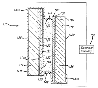
Figure 3 shows a cross-sectional view of mirror assembly 110 having a front
transparent element 112 having a front surface 112a and a rear surface 112b,
and a rear
element 114 having a front surface 114a and a rear surface 114b. For clarity
of
description of such a structure, the following designations will be used
hereinafter. The
front surface 112a of the front glass element will be referred to as the first
surface and
the back surface 112b of the front glass element as the second surface. The
front
surface 114a of the rea' glass element will be referred to as the third
surface, and the
back surface 114b of the rear glass element as the fourth surface. Chamber 125
is
defined by a layer of transparent conductor 128 (disposed on second surface
112b), a
reflector/electrode 120 (disposed on third surface 114a), and an inner
circumferential
wall 132 of sealing member 116.
Front transparent element 112 may be any material which is transparent and
9
SUBSTITUTE SHEET (RULE 26)
= CA 02284542 1999-09-20
WO 98/44385 PCT/US98/05989
has sufficient strength to be able to operate in the conditions, e.g., varying
temperatures and pressures, commonly found in the automotive environment.
Front
element 112 may comprise any type of borosilicate glass, soda lime glass,
float glass
or any other material, such as, for example, a polymer or plastic, that is
transparent in
the visible region of the electromagnetic spectrum. Front element 112 is
preferably a
sheet of glass. Rear element must meet the operational conditions outlined
above,
except that it does not need to be transparent, and therefore may comprise
polymers,
metals, glass, ceramics, and preferably is a sheet of glass.
The coatings of the third surface 114a are sealably bonded to the coatings on
1 o the second surface 112b in a spaced-apart and parallel relationship by a
seal member
116 disposed near the outer perimeter of both second surface 112b and third
surface
114a. Seal member 116 may be any material that is capable of adhesively
bonding the
coatings on the second surface 112b to the coatings on the third surface 1 14a
to seal
the perimeter such that electrochromic material 126 does not leak from chamber
125.
Optionally, the layer of transparent conductive coating 128 and the layer of
reflector/electrode 120 may be removed over a portion where the seal member is
disposed (not the entire portion, otherwise the drive potential could not be
applied to
the two coatings). In such a case, seal member 116 must bond well to glass.
The performance requirements for a perimeter seal member 116 used in an
2o electrochromic device are similar to those for a perimeter seal used in a
liquid crystal
device (LCD) which are well known in the art. The seal must have good adhesion
to
glass, metals and metal oxides, must have low permeabilities for oxygen,
moisture
vapor and other detrimental vapors and gases, and must not interact with or
poison the
electrochromic or liquid crystal material it is meant to contain and protect.
The
perimeter seal can be applied by means commonly used in the LCD industry such
as
by silk-screening or dispensing. Totally hermetic seals such as those made
with glass
frit or solder glass can be used, but the high temperatures involved in
processing
(usually near 450-degrees Centigrade) this type of seal can cause numerous
problems
such as glass substrate warpage, changes in the properties of transparent
conductive
3o electrode and oxidation or degradation of the reflector. Because of their
lower
processing temperatures, thermoplastic, thermosetting or UV curing organic
sealing
resins are preferred. Such organic resin sealing systems for LCD's are
described in
SUBSTITUTE SHEET (RULE 26)
- -------T..
CA 02284542 1999-09-20
WO 98/44385 PCTIUS98/05989
U.S. Patent Numbers 4,297,401, 4,418,102, 4,695,490, 5,596,023 and 5,596,024.
Because of their excellent adhesion to glass, low oxygen permeability and good
solvent resistance, epoxy based organic sealing resins are preferred. These
epoxy
resin seals may be UV curing, such as described in U.S. Patent Number
4,297,401, or
thermally curing, such as with mixtures of liquid epoxy resin with liquid
polyamide
resin or dicyandiamide, or they can be homopolymerized. The epoxy resin may
contain fillers or thickeners to reduce flow and shrinkage such as fumed
silica, silica,
mica, clay, calcium carbonate, alumina, etc., and/or pigments to add color.
Fillers
pretreated with hydrophobic or silane surface treatments are preferred. Cured
resin
io crosslink density can be controlled by use of mixtures of mono-functional,
di-
functional and multi-functional epoxy resins and curing agents. Additives such
as
silanes or titanates can be used to improve the seal's hydrolytic stability,
and spacers
such as glass beads or rods can be used to control final seal thickness and
substrate
spacing. Suitable epoxy resins for use in a perimeter seal member 116 include
but are
not limited to: "EPON RESIN" 813, 825, 826, 828, 830, 834, 862, 1001F, 1002F,
2012, DPS-155, 164, 1031, 1074, 58005, 58006, 58034, 58901, 871, 872 and DPL-
862 available from Shell Chemical Co., Houston, Texas; "ARALITE" GY 6010, GY
6020, CY 9579, GT 7071, XU 248, EPN 1139, EPN 1138, PY 307, ECN 1235, ECN
1273, ECN 1280, MT 0163, MY 720, MY 0500, MY 0510 and PT 810 available from
Ciba Geigy, Hawthorne, NY; "D.E.R." 331, 317, 361, 383, 661, 662, 667, 732,
736,
"D.E.N." 431, 438, 439 and 444 available from Dow Chemical Co., Midland,
Michigan. Suitable epoxy curing agents include V-15, V-25 and V-40 polyamides
from Shell Chemical Co.; "AJICURE" PN-23, PN-34 and VDH available from
Ajinomoto Co., Tokyo, Japan; "CUREZOL" AMZ, 2MZ, 2E4MZ, CI1Z, C17Z, 2PZ,
21Z and 2P4MZ available from Shikoku Fine Chemicals, Tokyo, Japan; "ERISYS"
DDA or DDA accelerated with U-405, 24EMI, U-410 and U-415 available from CVC
Specialty Chemicals, Maple Shade, NJ.; "AMICURE" PACM, 352, CG, CG-325 and
CG-1200 available from Air Products, Allentown, PA. Suitable fillers include
fumed
silica such as "CAB-O-SIL" L-90, LM-130, LM-5, PTG, M-5, MS-7, MS-55, TS-720,
3o HS-5, EH-5 available from Cabot Corporation, Tuscola, IL; "AEROSIL" R972,
R974,
R805, R812, R812 S, R202, US204 and US206 available from Degussa, Akron, OH.
Suitable clay fillers include BUCA, CATALPO, ASP NC, SATINTONE 5,
SUBSTITUTE SHEET (RULE 26)
~ CA 02284542 1999-09-20
WO 98/44385 PCr/US98/05989
SATINTONE SP-33, TRANSLINK 37, TRANSLINK 77, TRANSLINK 445,
TRANSLINK 555 available from Engelhard Corporation, Edison, NJ. -Suitable
silica
fillers are SILCRON G-130, G-300, G-100-T and G-100 available from SCM
Chemicals, Baltimore, MD. Suitable silane coupling agents to improve the
seal's
hydrolytic stability are Z-6020, Z-6030, Z-6032, Z-6040, Z-6075 and Z-6076
available from Dow Corning Corporation, Midland, MI. Suitable precision glass
microbead spacers are available in an assortment of sizes from Duke
Scientific, Palo
Alto, CA.
The layer of a transparent electrically conductive material 128 is deposited
on
lo the second surface 112b to act as an electrode. Transparent conductive
material 128
may be any material which bonds well to front element 112, is resistant to
corrosion
to any materials within the electrochromic device, resistant to corrosion by
the
atmosphere, has minimal diffuse or specular reflectance, high light
transmission, near
neutral coloration and good electrical conductance. Transparent conductive
material
128 may be fluorine doped tin oxide, tin doped indium oxide (ITO),
ITO/metaVITO
(IMI) as disclosed in "Transparent Conductive Multilayer-Systems for FPD
Applications", by J. Stollenwerk, B. Ocker, K.H. Kretschmer of LEYBOLD AG,
Alzenau, Germany, and the materials described in above-referenced U.S. Patent
No.
5,202,787, such as TEC 20 or TEC 15, available from Libbey Owens-Ford Co. of
2o Toledo, OH. Generally, the conductance of transparent conductive material
128 will
depend on its thickness and composition. IMI generally has superior
conductivity
compared with the other materials. IMI is, however, more difficult and
expensive to
manufacture and may be useful when high conductance is necessary. The
thickness of
the various layers in the IMI structure may vary but generally the thickness
of the first
ITO layer ranges from about 10 A to about 200 A the metal ranges from about 10
A to
about 200 A and the second layer of ITO ranges from about 10 A to about 200 A.
If
desired, an optional-layer or layers of a color suppression material 130 may
be
deposited between transparent conductive material 128 and the second surface
112b to
suppress the reflection of any unwanted portions of the electromagnetic
spectrum.
In accordance with the present invention, a combination reflector/electrode
120 is disposed on third surface 114a. Reflector/electrode 120 comprises at
least one
layer of a highly reflective material 121 which serves as a mirror reflectance
layer
12
SUBSTITUTE SHEET (RULE 26)
CA 02284542 1999-09-20
WO 98/44385 PCT/US98/05989
and also forms an integral electrode in contact with and in a chemically and
electrochemically stable relationship with any constituents in an
electrochromic
medium. As stated above, the conventional method of building electrochromic
devices was to incorporate a transparent conductive material on the third
surface as an
electrode, and place a reflector on the fourth surface. By combining the
"reflector"
and "electrode" and placing both on the third surface several unexpected
advantages
arise which not only make the device manufacture less complex, but also allow
the
device to operate with higher performance. The following will outline the
exemplary
advantages of the combined reflector/electrode of the present invention.
First, the combined reflector/electrode 120 on the third surface generally has
higher conductance than a conventional transparent electrode and previously
used
reflector/electrodes which will allow greater design flexibility. One can
either change
the composition of the transparent conductive electrode on the second surface
to one
that has lower conductance (being cheaper and easier to produce and
manufacture)
while maintaining coloration speeds similar to that obtainable with a fourth
surface
reflector device, while at the same time decreasing substantially the overall
cost and
time to produce the electrochromic device. If, however, performance of a
particular
design is of utmost importance, a moderate to high conductance transparent
electrode
can be used on the second surface, such as, for example, ITO, IMI, etc. The
combination of a high conductance reflector/electrode on the third surface and
a high
conductance transparent electrode on the second surface will not only produce
an
electrochromic device with more even overall coloration, but will also allow
for
increased speed of coloration and clearing. Furthermore, in fourth surface
reflector
mirror assemblies there are two transparent electrodes with relatively low
conductance
and in previously used third surface reflector mirrors there is a transparent
electrode
and a reflector/electrode with relatively low conductance and, as such, a long
buss bar
on the front and rear element to bring current in and out is necessary to
ensure
adequate coloring speed. The third surface reflector/electrode of the present
invention
has a higher conductance and therefore has a very even voltage or potential
3o distribution across the conductive surface, even with a small or irregular
contact area.
Thus the present invention provides greater design flexibility by allowing the
electrical contact for the third surface electrode to be very small while
still
13
SUBSTITUTE SHEET (RULE 26)
CA 02284542 1999-09-20
WO 98/44385 PCT/US98/05989
maintaining adequate coloring speed.
Second, a third surface reflector/electrode helps improve the image being
viewed through the mirror. Figure 1 shows how light travels through a
conventional
fourth surface reflector device. In the fourth surface reflector the light
travels through:
the first glass element; the transparent conductive electrode on the second
surface; the
electrochromic media; the transparent conductive electrode on the third
surface; and
the second glass element, before being reflected by the fourth surface
reflector. Both
transparent conductive electrodes exhibit highly specular transmittance but
also
possess diffuse transmittance and reflective components, whereas the
reflective layer
1o utilized in any electrochromic mirror is chosen primarily for its specular
reflectance.
By diffuse reflectance or transmittance component we mean a material which
reflects
or transmits a portion of any light impinging on it according to Lambert's law
whereby the light rays are spread-about or scattered. By specular reflectance
or
transmittance component we mean a material which reflects or transmits light
impinging on it according to Snell's laws of reflection or refraction. In
practical
terms, diffuse reflectors and transmitters tends to slightly blur images,
whereas
specular reflectors show a crisp, clear image. Therefore, light traveling
through a
mirror having a device with a fourth surface reflector has two partial diffuse
reflectors
(on the second and third surface) which tend to blur the image, and a device
with a
third surface reflector/electrode of the present invention only has one
diffuse reflector
(on the second surface).
Additionally, because the transparent electrodes act as partial diffuse
transmitters, and the farther away the diffuse transmitter is from the
reflecting surface,
the more severe the blurring becomes, a mirror with a fourth surface reflector
appears
significantly more hazy than a mirror with a third surface reflector. For
example, in
the fourth surface reflector shown in Fig. 1, the diffuse transmitter on the
second
surface is separated from the reflector by the electrochromic material, the
second
conductive electrode and the second glass element. The diffuse transmitter on
the
third surface is separated from the reflector by the second glass element. By
incorporating a combined reflector/electrode on the third surface in
accordance with
the present invention, one of the diffuse transmitters is removed and the
distance
between the reflector and the remaining diffuse transmitter is closer by the
thickness
14
SUBSTITUTE SHEET (RULE 26)
-.
7 ----
CA 02284542 1999-09-20
WO 98/44385 PCT/US98/05989
of the rear glass element. Therefore the third surface metal
reflector/electrode of the
present invention provides an electrochromic mirror with a superior viewing
image.
Finally, a third surface metal reflector/electrode improves the ability to
reduce
double imaging in an electrochromic mirror. As stated above, there are several
interfaces where reflections can occur. Some of these reflections can be
significantly
reduced with color suppression or anti-reflective coatings; however, the most
significant "double imaging" reflections are caused by misalignment of the
first
surface and the surface containing the reflector, and the most reproducible
way of
minimizing the impact of this reflection is by ensuring both glass elements
are
1o parallel. Presently, convex glass is often used for the passenger side and
aspheric
glass is sometimes used for the driver side mirror to increase the field of
view and
reduce potential blind spots. However, it is difficult to reproducibly bend
successive
elements of glass having identical radii of curvature. Therefore, when
building an
electrochromic mirror the front glass element and the rear glass element may
not be
perfectly parallel (do not have identical radii of curvature) and, therefore,
the
otherwise controlled double imaging problems become much more pronounced. By
incorporating a combined reflector electrode on the third surface of the
device in
accordance with the present invention, light does not have to travel through
the rear
glass element before being reflected, and any double imaging that occurs from
the
2o elements being out of parallel will be significantly reduced.
It is desirable in the construction of outside rearview mirrors to incorporate
thinner glass in order to decrease the overall weight of the mirror so that
the
mechanisms used to manipulate the orientation of the mirror are not
overloaded.
Decreasing the weight of the device also improves the dynamic stability of the
mirror
assembly when exposed to vibrations. Heretofore, no electrochromic mirrors
incorporating a solution-phase electrochromic medium and two thin glass
elements
have been commercially available because thin glass suffers from being
flexible and
prone to warpage or breakage, especially when exposed to extreme environments.
This problem is substantially improved by using an improved electrochromic
device
incorporating two thin glass elements having an improved gel material. This
improved device is disclosed in commonly assigned U.S. Patent Application
entitled
"AN ELECTROCHROMIC MIRROR WITH TWO THIN GLASS ELEMENTS
SUBSTITUTE SHEET (RULE 26)
= CA 02284542 1999-09-20
WO 98/44385 PCT/US98/05989
AND A GELLED ELECTROCHROMIC MEDIUM", filed on or about April 2, 1997.
The entire disclosure, including the references contained therein, of this
U.S. Patent
Application is hereby incorporated herein by reference. The addition of the
combined
reflector/electrode onto the third surface of the device further helps remove
any
residual double imaging resulting from the two glass elements being out of
parallel.
The most important factors for obtaining a reliable electrochromic mirror
having a third surface reflector/electrode 120 are that the
reflector/electrode have
sufficient reflectance and that the mirror incorporating the
reflector/electrode have
adequate operational life. Regarding reflectance, the auto manufacturer's
require a
highly reflective mirror for the inside mirror having a minimum reflectivity
of at least
70 percent, whereas the reflectivity requirements for an outside mirrors are
less
stringent and generally must be at least 50 percent. To produce an
electrochromic
mirror with 70% reflectance the reflector must have a higher reflectance
because
having the electrochromic medium in contact with the reflector will reduce the
reflectance from that interface as compared to having the reflector in air due
to the
medium having a higher index of refraction as compared to air. Also, the
glass, the
transparent electrode and the electrochromic medium even in its clear state
are slightly
light absorbing. Typically, if an overall reflectance of 70% is desired, the
reflector
must have a reflectance of about 80%. Therefore, highly reflectance in the
context of
the present invention means a reflector whose reflectance in air is at least
80%.
Regarding operational life, the layer or layers that comprise the
reflector/electrode 120 must have adequate bond strength to the peripheral
seal, the
outermost layer must have good shelf life between the time it is coated and
the time
the mirror is assembled, the layer or layers must be resistant to atmospheric
and
electrical contact corrosion, and must bond well to the glass surface or to
other layers
disposed beneath it, e.g., the base or intermediate layer (122 or 123,
respectively).
The overall sheet resistance for the reflector/electrode 120 may range from
about 0.01
/ to about 20 / and preferably ranges from about 0.2 / to about 6 / . As will
be discussed in more detail below, improved electrical interconnections using
a
portion of the third surface reflector/electrode as a high conductance contact
or buss
bar for the second surface transparent conductive electrode may be utilized
when the
conductance of the third surface reflector/electrode is below about 2/.
16
SUBSTITUTE SHEET (RULE 26)
T
CA 02284542 2004-10-29
Referring to Figure 3 for one embodiment of the present invention, a
reflector/electrode that is made from a single layer of a highly reflective
silver alloy 121
is provided that is in contact with at least one solution-phase electrochromic
material.
The layer of silver alloy covers the entire third surface 114a of second
element 114,
provided that a section of the reflector/electrode may be removed for a
display device
and a glare sensor, in accordance with applicant's U.S. Patent 5,825,527
entitled "AN
INFORMATION DISPLAY AREA ON ELECTROCHROMIC MIRRORS HAVING
A THIRD SURFACE REFLECTOR" issued October 20, 1998. The highly reflective
silver alloy means a homogeneous or non-homogeneous mixture of silver and one
or
more metals, or an unsaturated, saturated or supersaturated solid solution of
silver and
one or more metals. The thickness of highly reflective layer 121 ranges from
about 50
A to about 2000 A and more preferably from about 200 A to about 1000 A. If
highly
reflective layer 121 is disposed directly to the glass surface, it is
preferred that the glass
surface be treated by plasma discharge to improve adhesion.
Table I shows the relevant properties for a number of different metals that
have
been proposed for third surface reflectors as compared with the materials
suitable for
the reflector/electrode 120 of the present invention. The only materials in
Table I
having reflectance properties suitable for use as a third surface
reflector/electrode in
contact with at least one solution-phase electrochromic material for an inside
electrochromic mirror for a motor vehicle are aluminum, silver, and silver
alloys.
Aluminum performs very poorly when in contact with solution-phase material(s)
in the
electrochromic medium because aluminum reacts with or is corroded by these
materials. The reacted or corroded aluminum is non-reflective and non-
conductive and
will typically dissolve off, flake off or delaminate from the glass surface.
Silver is more
stable than aluminum but can fail when deposited over the entire third surface
because
it does not have long shelf life and is not resistant to electrical contact
corrosion when
exposed to the environmental extremes found in the motor vehicle environment.
These
environmental extremes include temperatures ranging from about -40 C to
about 85 C,
and humidities ranging from about 0 percent to about 100 percent. Further,
mirrors
must survive at these temperatures and humidities for coloration cycle lives
up to
100,000 cycles. The other prior art
17
= CA 02284542 1999-09-20
WO 98/44385 PCT/US98/05989
materials (silver/copper, chromium, stainless steel, rhodium, platinum,
palladium,
Inconel , copper or titanium) suffer from any one of a number of deficiencies
such
as: very poor color neutrality (silver/copper and copper); poor reflectance
(chromium,
stainless steel, rhodium, platinum, palladium, Inconel , and titanium); or
poor
cleanability (chromium).
When silver is alloyed with certain materials to produce a third surface
reflector/electrode the deficiencies associated with silver metal and aluminum
metal
can be overcome. Suitable materials for the reflective layer are alloys of
silver/palladium, silver/gold, silver/platinum, silver/rhodium,
silver/titanium, etc.
lo The amount of the solute material, i.e., palladium, gold, etc., can vary.
As can be seen
from Table 1, the silver alloys surprisingly retain the high reflectance and
low sheet
resistance properties of silver, while simultaneously improving their contact
stability,
shelf life and also increasing their window of potential stability when used
as
electrodes in propylene carbonate containing 0.2 molar tetraethylammonium
tetrafluoroborate. The presently preferred materials for highly reflective
layer 121 are
Ag/Au, Ag/Pt and Ag/Pd.
More typically, reflector/electrode 120 has, in addition to the layer of a
highly
reflective alloy 121, an optional base layer of a conductive metal or alloy
122
deposited directly on the third surface 114a. There may also be an optional
intermediate layer of a conductive metal or alloy 123 disposed between the
layer of
highly reflective material 121 and the base coat 122. If reflector/electrode
120
includes more than one layer there should not be galvanic corrosion between
the two
metals or alloys. If optional base layer 122 is deposited between the highly
reflective
layer 121 and the glass element 114, it should be environmentally rugged,
e.g., bond
well to the third (glass) surface 114a and to highly reflective layer 121, and
maintain
this bond when the seal 116 is bonded to the reflective layer. Base layer 122
should
have a thickness from about 50 A to about 2000 A and more preferably from
about
100 A to about 1000 A. Suitable materials for the base layer 122 are chromium,
stainless steel, titanium, and alloys of chromium/molybdenum/nickel,
molybdenum
and nickel-based alloys (commonly referred to as Inconel(V, available from
Castle
Metals, Chicago, IL). The main constituents of Inconel are nickel which may
range
from 52% to 76% (Inconel(b 617 and 600, respectfully), iron which may range
from
18
SUBSTITUTE SHEET (RULE 26)
CA 02284542 1999-09-20
WO 98/44385 PCT/US98/05989
1.5% to 18.5% (Inconel 617 and Inconel 718, respectfully) and chromium which
may range from 15% to 23% (Inconel 600 and Inconel 601, respectfully).
Inconel 617 having 52% nickel, 1.5% iron, 22% chromium, and typical "other"
constituents including 12.5% cobalt, 9.0% molybdenum and 1.2% aluminum was
used in the present examples.
In some instances it is desirable to provide an optional intermediate layer
123
between the highly reflective layer 121 and the base layer 122 in case the
material of
layer 121 does not adhere well to the material of layer 122 or there are any
adverse
interactions between the materials, e.g., galvanic corrosion. If used,
intermediate
1o layer 123 should exhibit environmental ruggedness, e.g., bond well to the
base layer
122 and to the highly reflective layer 121, and maintain this bond when the
seal
member 116 is bonded to the highly reflective layer 121. The thickness of
intermediate layer 123 ranges from about 50 A to about 2000 A and more
preferably
from about 100 A to about 1000 A. Suitable materials for the optional
intermediate
layer 123 are molybdenum, rhodium, stainless steel, titanium, copper, nickel
and
platinum. Reference is made to examples 1 and 2 to show how the insertion of a
rhodium intermediate layer between a chromium base layer and a silver or
silver alloy
reflective layer increases the time to failure in copper-accelerated acetic
acid-salt
spray (CASS) by a factor of 10. Example 4 shows how the insertion of a
molybdenum intermediate layer between a chromium base layer and a silver alloy
having a molybdenum flash over-coat layer increases the time to failure in
CASS by a
factor of 12.
Finally, it is sometimes desirable to provide an optional flash over-coat 124
over highly reflective layer 121 such that it (and not the highly reflective
layer 121)
contacts the electrochromic medium. This flash over-coat layer 124 must have
stable
behavior as an electrode, it must have good shelf life, it must bond well to
the highly
reflective layer 121 and maintain this bond when the seal member 116 is bonded
thereto. It must be sufficiently thin such that it does not completely block
the
reflectivity of highly reflective layer 121. In accordance with another
embodiment of
the present invention, when a very thin flash over-coat 124 is placed over the
highly
reflecting layer, then the highly reflective layer 121 may be silver metal or
a silver
alloy because the flash layer protects the highly reflective layer while still
allowing
19
SUBSTITUTE SHEET (RULE 26)
= CA 02284542 1999-09-20
WO 98/44385 PCT/US98/05989
the highly reflecting layer 121 to contribute to the reflectivity of the
mirror. In such
cases a thin (between about 25 A and about 300 A) layer of rhodium, platinum
or
molybdenum is deposited over the highly reflective layer 121.
It is preferred but not essential that the third surface reflector/electrode
120 be
maintained as the cathode in the circuitry because this eliminates the
possibility of
anodic dissolution or anodic corrosion that might occur if the
reflector/electrode was
used as the anode. Although as can be seen in the Table, if certain silver
alloys are
used the positive potential limit of stability extends out far enough, e.g.,
1.2 V, that
the silver alloy reflector/electrode could safely be used as the anode in
contact with at
1 o least one solution-phase electrochromic material.
SUBSTITUTE SHEET (RULE 26)
Patent Application AUTO 616
0
TABLE ] A
o~o
White Light
Reflectance Reflectance Contact Negative Potential Limit Positive Potential
Limit
Metal In Air In Device Stability of Window of Potential Window of Potential
(%) Stability (V) Stability (V)
Al >92 N/A Very poor N/A N/A
cn y
y Cr 65 N/A Poor N/A N/A
Stainless 60 N/A Good N/A N/A
Steel
m Rh 75 N/A Very good N/A N/A
N
m Pt 72 N/A Very good N/A N/A
m
Inconel 55 N/A N/A N/A N/A
m
r Ag 97 84 Fair -2.29 0.86
m
Ag2.7Pd 93 81 Good -2.26 0.87
...
Ag l OPd 80 68 Good -2.05 0.97
Ag6Pt 92 80 Good -1.66* 0.91
Ag6Au 96 84 Good -2.25 0.98
Ag l 5Au 94 82 Good -2.3 1.2
y
This number is suspect because the test was run in propylene carbonate
containing some water.
cn
No
00
= CA 02284542 1999-09-20
WO 98/44385 PCT/OS98/05989
The various layers of reflector/electrode 120 can be deposited by a variety of
deposition procedures, such as RF and DC sputtering, e-beam evaporation,
chemical
vapor deposition, electrodeposition, etc., that will be known to those skilled
in the art.
The preferred alloys are preferably deposited by sputtering (RF or DC) a
target of the
desired alloy or by sputtering separate targets of the individual metals that
make up
the desired alloy such that the metals mix during the deposition process and
the
desired alloy is produced when the mixed metals deposit and solidify on the
substrate
surface.
In another embodiment, the reflector/electrode 120, shown in Figure 4, has at
least two layers (121 and 122) where at least one layer of a base material 122
covers
the entire portion of the third surface 1 14a (except for sections removed for
a display
device and a glare sensor in accordance with the U.S. Patent Application
entitled "AN
INFORMATION DISPLAY AREA ON ELECTROCHROMIC MIRRORS HAVING
A THIRD SURFACE REFLECTOR") and at least one layer of a highly reflective
material 121 covers the inner section of the third surface 1 l4a but does not
cover the
peripheral edge portion 127 where seal member 116 is disposed. Peripheral
portion
127 may be created by masking that portion of layer 122 during deposition of
the
layer of highly reflective material 121, or the layer of highly reflective
material may
be deposited over the entire third surface and subsequently removed or
partially
removed in the peripheral portion. The masking of layer 122 may be
accomplished
by use of a physical mask or through other well known techniques such as
photolithography and the like. Altematively, layer 122 may be partially
removed in
the peripheral portion by a variety of techniques, such as, for example, by
etching
(laser, chemical or otherwise), mechanical scraping, sandblasting or
otherwise. Laser
etching is the presently preferred method because of its accuracy, speed and
control.
Partial removal is preferably accomplished by laser etching in a pattern where
enough
metal is removed to allow the seal member 116 to bond directly to the third
surface
114a while leaving enough metal in this area such that the conductance in this
area is
not significantly reduced. For example, the metal may be removed in a dot
pattem or
other pattern as taught for removal of metal for information display in the
immediately above-referenced U.S. Patent Application.
In addition, an optional intermediate layer of a conductive material 123 may
22
SUBSTITUTE SHEET (RULE 26)
T
CA 02284542 2004-10-29
be placed over the entire area of third surface 114a and disposed between the
highly
reflective layer 121 and the base layer 122, or it may be placed only under
the area
covered by layer 121, i.e., not in peripheral edge portion 127. If this
optional
intermediate layer is utilized, it can cover the entire area of third surface
114a or it may
be masked or removed from peripheral edge portion as discussed above.
An optional flash over-coat layer 124 may be coated over the highly reflective
layer 121. The highly reflective layer 121, the optional intermediate layer
123 and the
base layer 122 preferably have properties similar to that described above,
except that
the layer of highly reflective material 121 need not bond well to the epoxy
seal since it
is removed in the peripheral portion where seal member is 116 placed. Because
the
interaction with the epoxy seal is removed, silver metal itself, in addition
to the alloys
of silver described above, will function as the highly reflective layer.
Referring again to Figure 3, chamber 127, defined by transparent conductor 128
(disposed on front element rear surface 112b), reflector/electrode 120
(disposed on rear
element front surface 114a), and an inner circumferential wall 132 of sealing
member
116, contains an electrochromic medium 126. Electrochromic medium 126 is
capable
of attenuating light traveling therethrough and has at least one solution-
phase
electrochromic material in intimate contact with reflector/electrode 120 and
at least one
additional electroactive material that may be solution-phase, surface-
confined, or one
that plates out onto a surface. However, the presently preferred media are
solution
phase redox electrochromics, such as those disclosed in above-referenced U.S.
Patent
Nos. 4,902,108; 5,128,799; 5,278,693; 5,280,380; 5,282,077; 5,294,376;
5,336,448.
Applicant's Canadian Patent Application 2,284,538 entitled "AN IMPROVED
ELECTROCHROMIC MEDIUM CAPABLE OF PRODUCING A PRE-SELECTED
COLOR" discloses electrochromic media that are perceived to be gray throughout
their
normal range of operation. If a solution-phase electrochromic medium is
utilized, it
may be inserted into chamber 125 through a sealable fill port 142 through well
known
techniques, such as vacuum backfilling and the like.
A resistive heater 138, disposed on the fourth glass surface 114b, may
optionally
be a layer of ITO, fluorine-doped tin oxide, or may be other heater layers or
structures
well known in the art. Electrically conductive spring clips 134a and
23
~ CA 02284542 1999-09-20
WO 98/44385 PCT/US98/05989
134b are placed on the coated glass sheets (112 and 114) to make electrical
contact
with the exposed areas of the transparent conductive coating 128 (clip 134b)
and the
third surface reflector/electrode 120 (clip 134a). Suitable electrical
conductors (not
shown) may be soldered or otherwise connected to the spring clips (134a and
134b) so
that a desired voltage may be applied to the device from a suitable power
source.
An electrical circuit 150, such as those taught in the above-referenced
Canadian Patent No. 1,300945 and U.S. Patent Nos. 5,204,778; 5,434,407; and
5,451,822, is connected to, and allows control of the potential to be applied
across,
reflector/electrode 120 and transparent electrode 128 such that electrochromic
medium 126 will darken and thereby attenuate various amounts of light
traveling
therethrough and thus vary the reflectance of the mirror containing
electrochromic
medium 126.
As stated above, the low resistance of reflector/electrode 120 allows greater
design flexibility by allowing the electrical contact for the third surface
reflector/electrode to be small while maintaining adequate coloring speed.
This
flexibility extends to improving the interconnection techniques to the layer
of
transparent conductive material 128 on the second surface 112b. Referring now
to
Figures 5a and 5b, an improved mechanism for applying a drive potential to the
layer
of transparent conductive material 128 is shown. Electrical connection between
the
power supply and the layer of transparent conductive material 128 is made by
connecting the buss bars (or clips I 19a) to the area of reflector/electrode
120a such
that the drive potential travels through the area of reflector/electrode 120a
and the
conductive particles 116b in sealing member 116 before reaching the
transparent
conductor 128. Reflector/electrode must not be present in area 120c so that
there is no
chance of current flow from reflector/electrode area 120a to 120b. This
configuration
is advantageous in that it allows connection to the transparent conductive
material 128
nearly all the way around the circumference and therefore improves the speed
of
dimming and clearing of the electrochromic media 126.
In such a configuration, sealing member 116 comprises a typical sealing
material, e.g., epoxy 11 6a, with conductive particles 11 6b contained
therein. The
conductive particles may be small, such as, for example, gold, silver, copper,
etc.,
24
SUBSTITUTE SHEET (RULE 26)
-- ---__~ -- --
CA 02284542 1999-09-20
WO 98/44385 PCTiUS98/05989
coated plastic with a diameter ranging from about 5 microns to about 80
microns, in
which case there must be a sufficient number of particles to ensure sufficient
conductivity between the reflector/electrode area 120a and the transparent
conductive
material 128. Alternatively, the conductive particles may be large enough to
act as
spacers, such as, for example, gold, silver, copper, etc., coated glass or
plastic beads.
The reflector/electrode 120 is separated into two distinct reflector/electrode
areas
(120a and 120b, separated by an area 120c devoid of reflector/electrode).
There are
many methods of removing the reflector/electrode 120 from area 120c, such as,
for
example, chemical etching, laser ablating, physical removal by scraping, etc.
Deposition in area 120c can also be avoided by use of a mask during deposition
of
reflector/electrode. Sealing member 116 with particles 116b contacts area 120a
such
that there is a conductive path between reflector/electrode area 120a and the
layer of
transparent conductive material 128. Thus, electrical connection to the
reflector/electrode area 120b that imparts a potential to the electrochromic
medium is
connected through clips 119b to the electronic circuitry at
reflector/electrode area
120d (Figure 5b). No conductive particles 116b can be placed in this
reflector/electrode area 120b because of the possibility of an electrical
short between
reflector/electrode area 120b and the layer of transparent conductive material
128. If
such an electrical short occurred the electrochromic device would not operate
properly. Additionally, no conductive seal 116b should be present in area
120d.
A variety of methods can be used to ensure that no conductive particles 116b
enter into this reflector/electrode area 120b, such as, for example, disposing
a
nonconductive material into the area 120c of reflector/electrode devoid of
conductive
material. A dual dispenser could be used to deposit the seal 116 with
conductive
particles 116b onto reflector/electrode area 120a and simultaneously deposit
the
nonconductive material into reflector/electrode area 120c. Another method
would be
to cure a nonconductive seal in area 120c and then dispose a conductive
material 116c
into the edge gap to electrically interconnect reflector/electrode area 120a
with
transparent conductive layer 128. A general method of ensuring that no
conductive
particles reach reflector/electrode area 120b is to make sure seal 116 has
proper flow
characteristics such that the conductive portion 1 16b tents to stay behind as
the
sealant is squeezed out during assembly and only the non-conductive portion of
116
SUBSTITUTE SHEET (RULE 26)
= CA 02284542 1999-09-20
WO 98/44385 PCT/US98/05989
flows into area 120b. In an alternative embodiment, spacer member 116 need not
contain conductive particles and a conductive member or material 116c may be
placed
on or in the outer edge of member 116 to interconnect transparent conductive
material
128 to reflector/electrode area 120a.
Yet another embodiment of an improved electrical interconnection technique
is illustrated in Figure 6 where a first portion of seal member 116 is applied
directly
onto the third surface 114a and cured prior to the application of
reflector/electrode
120. After the reflector/electrode 120 is deposited onto the third surface
114a over
the first portion of seal member 116, a portion of the cured seal member 116
is
machined off to leave 116i as shown with a predetermined thickness (which will
vary
depending on the desired cell spacing between the second surface 112b and the
third
surface 114a). The cell spacing ranges from about 20 microns to about 400
microns,
and preferably range from about 90 microns to about 230 microns. By curing the
first
portion of seal member and machining it to a predetermined thickness (116i)
the need
for glass beads to ensure a constant cell spacing is eliminated. Glass beads
are useful
to provide cell spacing, however, they provide stress points where they
contact
reflector/electrode 120 and transparent conductor 128. By removing the glass
beads
these stress points are also removed. During the machining, the
reflector/electrode
120 that is coated on first portion of seal member 116 is removed to leave an
area
devoid of reflector/electrode 120. A second portion of seal member 116ii is
then
deposited onto the machined area of the first portion of seal member 116i or
on the
coatings on second surface 112b in the area corresponding to 116i, and seal
member
116ii is cured after assembly in a conventional manner. Finally, an outer
conductive
seal member 117 may optionally be deposited on the outer peripheral portion of
seal
member 116 to make electrical contact between the outer edge of
reflector/electrode
120 and the outer peripheral edge of the layer of transparent conductive
material 128.
This configuration is advantageous in that it allows connection to the
transparent
conductive material 128 nearly all the way around the circumference and
therefore
improves the speed of dimming and clearing of the electrochromic media 126.
Referring again to Figure 2, rearview mirrors embodying the present invention
preferably include a bezel 144, which extends around the entire periphery of
each
individual assembly 110, 111a and/or 11 lb. The bezel 144 conceals and
protects
26
SUBSTITUTE SHEET (RULE 26)
CA 02284542 1999-09-20
WO 98/44385 PCTlUS98/05989
the spring clips 134a and 134b of Fig. 3, (or 116a and 116b of Fig. 5a,'116i,
116ii and
117 of Fig. 6) and the peripheral edge portions of sealing member and both the
front
and rear glass elements (112 and 114, respectively). A wide variety of bezel
designs
are well known in the art, such as, for example the bezel taught and claimed
in above-
referenced U.S. Patent No. 5,448,397. There are also a wide variety of housing
well
known in the art for attaching the mirror assembly 110 to the inside front
windshield
of a n automobile, or f o r attaching the mirror assemblies l l la and III b
to the outside
of an automobile. A preferred mounting bracket is disclosed in above-
referenced U.S.
Patent No. 5,337,948.
The electrical circuit preferably incorporates an ambient light sensor (not
shown) and a glare light sensor 160, the glare light sensor being positioned
either
behind the mirror glass and looking through a section of the mirror with the
reflective
material completely or partially removed, or the glare light sensor can be
positioned
outside the reflective surfaces, e.g., in the bezel 144. Additionally, an area
or areas of
the electrode and reflector, such as 146, may be completely removed, or
partially
removed in, for example, a dot or line pattern, to permit a vacuum fluorescent
display,
such as a compass, clock, or other indicia, to show through to the driver of
the
vehicle. Above-referenced co-filed U.S. Patent Application entitled "AN
INFORMATION DISPLAY AREA ON ELECTROCHROMIC MIRRORS HAVING
A THIRD SURFACE REFLECTOR" shows a presently preferred line pattern. The
present invention is also applicable to a mirror which uses only one video
chip light
sensor to measure both glare and ambient light and which is further capable of
determining the direction of glare. An automatic mirror on the inside of a
vehicle,
constructed according to this invention, can also control one or both outside
mirrors as
slaves in an automatic mirror system
The following illustrative examples are not intended to limit the scope of the
present
invention but to illustrate its application and use:
EXAMPLE 1
Electrochromic mirror devices incorporating a high reflectivity third surface
reflector/electrode were prepared by sequentially depositing approximately 700
angstroms of chromium and approximately 500 angstroms of silver on the surface
of
27
SUBSTITUTE SHEET (RULE 26)
= CA 02284542 1999-09-20
WO 98/44385 PCT/US98/05989
2.3 millimeter thick sheets of flat soda lime float glass cut to an automotive
mirror
element shape. A second set of high reflectivity third surface
reflector/electrodes were
also prepared by sequentially depositing 700 angstroms of chromium and
approximately 500 angstroms of a silver alloy containing 3% by weight
palladium on
the glass element shapes. The deposition was accomplished by passing the said
glass
element shapes past separate metal targets in a magnetron sputtering system
with a
base pressure of 3 x10'6 torr and an argon pressure of 3 x 10"3 torr.
The chromium/silver and chromium/silver 3% palladium alloy coated glass
automotive mirror shapes were used as the rear planar elements of an
electrochromic
mirror device. The front element was a sheet of TEC 15 transparent conductor
coated
glass from LOF cut similar in shape and size to the rear glass element. The
front and
rear elements were bonded together by an epoxy perimeter seal with the
conductive
planar surfaces facing each other and parallel to each other with an offset.
The
spacing between the electrodes was about 137 microns. The devices were vacuum
filled through a fill port left in the perimeter seal with an electrochromic
solution
made up of:
0.028 molar 5,10-dihydro-5-10-dimethylphenazine
0.034 molar 1,1'-di(3-phenyl(n-propane))-4,4'-bipyridinium
di(tetrafluoroborate)
0.030 molar 2-(2'-hydroxy-5'-methylphenyl)-benzotriazole
in a solution of 3 weight percent ElvaciteTM 2051 polymethylmethacrylate
resin dissolved in propylene carbonate.
The fill port was plugged with a UV cure adhesive which was cured by
exposure to UV light.
The devices were subjected to accelerated durability tests until the seal
integrity of the device was breached or the lamination of the
reflector/electrode layers
or the transparent electrode layers were substantially degraded or dilapidated
at which
time the said device is said to fail. The first test performed was steam
autoclave
testing in which the devices were sealed in a water containing vessel and
subjected to
120 degrees centigrade at a pressure of 15 pounds per square inch (psi). The
second
test performed was copper-accelerated acetic acid-salt spray (CASS) as
described in
ASTM B 368-85.
28
SUBSTITUTE SHEET (RULE 26)
CA 02284542 1999-09-20
WO 98/44385 PCT/US98/05989
When the electrochromic devices were observed after one day in testing, all of
the devices failed to withstand the CASS testing and all of the devices failed
to
withstand the steam autoclave testing.
EXAMPLE 2
Other than as specifically mentioned, the devices in this example were
constructed in accordance with the conditions and teachings in example 1.
Multilayer
combination reflector/electrodes were prepared by sequentially depositing
approximately 700 angstroms chromium, approximately 100 angstroms rhodium and
approximately 500 angstroms of silver on the surface of said glass element
shapes. A
second set of multilayer combination reflector/electrodes were also prepared
by
sequentially depositing approximately 700 angstroms of chromium, approximately
100 angstroms rhodium and approximately 500 angstroms of a silver alloy
containing
3% by weight palladium on the surface of said glass element shapes. The
electrochromic devices were constructed and tested in accordance with example
1.
The device incorporating the sequential multilayer combination reflector
electrode of chromium, rhodium and silver withstood steam autoclave testing
two
times longer and CASS testing 10 times longer than device in example 1 before
failure occurred. The device incorporating the sequential multilayer
combination
reflector electrode of chromium, rhodium and silver 3% palladium alloy
withstood
steam autoclave testing three times longer and CASS testing 10 times longer
than
devices in example 1 before failure occurred.
EXAMPLE 3
Other than as specifically mentioned, the devices in this example were
constructed in
accordance with the conditions and teachings in example 1. Multilayer
combination
reflector/electrodes were prepared by sequentially depositing approximately
700
angstroms chromium, approximately 500 angstroms molybdenum and approximately
500 angstroms of a silver alloy containing 3% by weight palladium on the
surface of
29
SUBSTITUTE SHEET (RULE 26)
= CA 02284542 1999-09-20
WO 98/44385 PCT/US98/05989
said glass element shapes. The electrochromic devices were constructed and
tested in
accordance with example 1.
The device incorporating the sequential multilayer combination reflector
electrode of chromium, molybdenum and silver 3% palladium alloy withstood CASS
testing 10 times longer than devices in example 1 before failure occurred.
EXAMPLE 4
Other than as specifically mentioned, the devices in this example were
constructed in
accordance with the conditions and teachings in example 1. Multilayer
combination
reflector/electrodes were prepared by sequentially depositing approximately
700
angstroms chromium, approximately 500 angstroms of a silver alloy containing
3%
by weight palladium and approximately 100 angstroms of molybdenum on the
surface
of said glass element shapes. A second set of multilayer combination
reflector/electrodes were also prepared by sequentially depositing
approximately 700
angstroms of chromium, approximately 500 angstroms molybdenum, approximately
500 angstroms of a silver alloy containing 3% by weight palladium and
approximately
100 angstroms of molybdenum on the surface of said glass element shapes. The
electrochromic devices were constructed and tested in accordance with example
1.
The device incorporating the sequential multilayer combination reflector
electrode of chromium, molybdenum, silver 3% palladium, molybdenum withstood
steam autoclave testing 25% longer and CASS testing twelve times longer than
the
sequential multilayer combination reflector electrode device of chromium,
silver 3%
palladium, molybdenum before failure occurred. Also, the device incorporating
the
sequential multilayer combination reflector electrode of chromium, molybdenum,
silver 3% palladium, molybdenum withstood CASS testing three times longer than
the
device constructed in-rxample 3. Finally, the sequential multilayer
combination
reflector electrode device of chromium, silver 3% palladium, molybdenum
withstood
two times longer in CASS testing and twenty times longer in steam autoclave
testing
than the sequential multilayer combination reflector electrode device of
chromium,
silver 3% palladium of example 1.
EXAMPLE 5
SUBSTITUTE SHEET (RULE 26)
CA 02284542 1999-09-20
WO 98/44385 PCT/US98/05989
Other than as specifically mentioned, the devices in this example were
constructed in
accordance with the conditions and teachings in example 1. Multilayer
combination
reflector/electrodes were prepared by sequentially depositing approximately
700
angstroms chromium, approximately 100 angstroms rhodium and approximately 500
angstroms of silver on the surface of said glass element shapes. A second set
of
multilayer combination reflector/electrodes were also prepared by sequentially
depositing approximately 700 angstroms of chromium, approximately 100
angstroms
rhodium and approximately 500 angstroms of a silver alloy containing 3% by
weight
palladium on the surface of said glass element shapes. A third set of
multilayer
combination reflector/electrodes were also prepared by sequentially depositing
approximately 700 angstroms of chromium, approximately 100 angstroms rhodium
and approximately 500 angstroms of a silver alloy containing 6% by weight
platinum
on the surface of said glass element shapes. A fourth set of multilayer
combination
reflector/electrodes were also prepared by sequentially depositing
approximately 700
angstroms of chromium, approximately 100 angstroms rhodium and approximately
500 angstroms of a silver alloy containing 6% by weight gold on the surface of
said
glass element shapes. A fifth set of multilayer combination
reflector/electrodes were
also prepared by sequentially depositing approximately 700 angstroms of
chromium,
approximately 100 angstroms rhodium and approximately 500 angstroms of a
silver
alloy containing 15% by weight gold on the surface of said glass element
shapes. The
electrochromic devices were constructed in accordance with example 1.
Conductive clips were connected to the offset portions of the front and rear
elements of the devices. A power source was connected to the clips and 1.2
volts was
applied to the devices continuously for approximately 250 hours at
approximately 20
degrees Celsius, with the connection arranged such that the
reflector/electrode was the
cathode. The device incorporating the sequential multilayer combination
reflector
electrode of chromium, rhodium and silver exhibited a yellowing effect within
the
electrochromic medium. This yellowing phenomenon was not apparent in any of
the
silver alloy devices.
While the invention has been described in detail herein in accordance with
certain preferred embodiments thereof, many modifications and changes therein
may
be effected by those skilled in the art without departing from the spirit of
the
31
SUBSTITUTE SHEET (RULE 26)
~ CA 02284542 1999-09-20
WO 98/44385 PCT/US98/05989
invention. Accordingly, it is our intent to be limited only by the scope of
the
appending claims and not by way of the details and instrumentalities
describing the
embodiments shown herein.
32
SUBSTITUTE SHEET (RULE 26)
__ -T_