Note: Descriptions are shown in the official language in which they were submitted.
CA 02284634 2005-06-16
CA 02284634 1999-09-20
WO 98143073 PCT/AU98100184
-1-
TITLE: "SENSOR CONNECTION MEANS"
TECHNICAL FIELD
This invention relates to disposable electrochemical sensors of the type used
for
5 quantitative analysis, for example, of glucose levels in blood, for pH
measurement, or the
tike. More particularly the invention relates to means for electrical
connection of such
sensors to a measuring apparatus.
BACKGROUND ART
US Patent 5,437,999 discloses an electrochemical sensor of the kind which in
use is
electrically connected with a power source. The sensor is constructed from two
spaced
apart printed circuit boards each having a metal layer on one side and
disposed so that the
metal layers are facing each other in spaced apart relationship. The metal
layers are
photolithographically treated to define electrode areas which form pan of a
cell. At one
end of the assembly the electrode substrates are cut to provide laterally
spaced protruding
15 tabs bearing the metal layer. The exposed metal surfaces of the tabs act as
contact pads,
each contact pad being electrically connected with a corresponding electrode.
The contact
pads in turn engage contact prongs connected to a power source and provide
electrical
connection between the sensor and a power source.
The arrangement of US Patent 5,437,999 suffers from the disadvantages that the
2o substrate is required to be of considerable rigidity in order to ensure
satisfactory and
reliable electrical contact. Moreover the user is often left uncertain as to
whether a sensor
has satisfactorily been connected with the power source.
In co-pending applications WO 96132635, WO 97/0041, WO 97/18465 and
WO 97/18464 there are described various very thin electrochemical cells. Each
__ _ CA 02284634 1999-09-20
WO 98/43073 PCT/AU98/00184
-2-
cell is defined between facing spaced apart electrodes which are formed as
thin metal
coatings (for example sputter coatings) deposited on thin inert plastic film
(for example
100 micron thick PET). The electrodes are separated one from the other by a
spacer of
thickness of for example 500 ~m or less.
The connection arrangement of US 5,437,999 is not suitable for use with the
extremely thin sensor devices of the kind discussed in our co-pending
applications in view
of the flexibility of the insulating electrode carriers. In general, it is
desirable that the
disposable sensor be capable of simple, quick, reliable and effective
connection with the
power source in the measuring device by unskilled users. It is an object of
the present
1 o invention to overcome or ameliorate at least one of the disadvantages of
the prior art, or to
provide a useful alternative.
DESCRIPTION OF THE INVENTION
According to a first aspect, the invention provides a sensor adapted for
electrical
connection with a power source having first contact means, the sensor
comprising:
15 a first insulating substrate carrying a first electrode and a second
insulating substrate
carrying a second electrode, said electrodes being disposed to face each other
in spaced
apart relationship,
a first cut-out portion extending through said first insulating substrate and
a spacer to
expose a first contact area on the second insulating substrate to permit a
first contact means
2o to effect electrical connection with the first contact area disposed on the
second insulating
substrate, the first contact area being in electrically conductive connection
with the second
electrode.
The first contact area may be maintained at a predetermined depth from the
first
insulating substrate.
CA 02284634 1999-09-20
WO 98/43073 PCT/AU98/00184
-3-
According to a second aspect, the invention provides a sensor according to the
first
aspect further comprising a second cut-out portion extending through said
second
insulating substrate and the, or another, spacer to expose a second contact
area on the first
insulating substrate to permit a second contact means to effect electrical
connection with a
second contact area disposed on the first insulating substrate, the second
contact area being
in electrically conductive connection with the first electrode.
The second contact area may be maintained at a predetermined depth from the
second insulating substrate.
According to a third aspect, the invention also provides a sensing system
comprising
1 o a sensor according to the first or second aspects and a sensing apparatus
including a first
contact means and/or second contact means adapted to effect electrical contact
with the
first and second contact areas respectively.
"Comprising" as herein used is used in an inclusive sense, that is to say in
the sense
of "including" or "containing". The term is not intended in an exclusive sense
("consisting
~ 5 of or "composed of')
In preferred embodiments the insulating substrate is made of a flexible
insulating
material. The second electrode and the first contact area are formed from a
unified layer of
metal deposited on the first substrate, and more preferably deposited by being
sputter
coated thereon. Suitable metals include, but are not limited to palladium,
gold, platinum,
' 2o iridium, and silver. Carbon may also be used. Desirably the contactor is
a metal contactor
which is resiliently biased to extend through the first cut-out portion to
make contact with
the metal first contact area on the second substrate. In highly preferred
embodiments the
contactor is adapted for click engagement with the cut-out portion which
extends through
the first insulating substrate and the spacer.
CA 02284634 1999-09-20
WO 98/43073 PCT/AU98/00184
-4-
With a connector according to the current invention the spacer layer provides
extra
strength. A rigid connector can therefore be formed using flexible materials.
This allows a
wider range of materials to be utilised. An audible confirmation of connection
can also be
simply provided by the current invention unlike the connector described in US
5,437,999.
BRIEF DESCRIPTION OF THE DRAWINGS
The invention will now be described by way of example only with reference to
the
accompanying drawings in which:
Figure 1 shows a first embodiment of a sensor according to the invention in
plan
mew.
Figure 2 shows a scrap side elevation of the sensor of Figure I in cross-
section on
line 10-10.
Figure 3 is a diagrammatic enlargement showing a part of the sensor of Figure
2 in
engagement with contacts.
Figure 4 shows an end elevation of the sensor of Figure 3 in section on line A-
A.
Figure 5 shows a second embodiment of the invention in plan view.
Figure 6 shows a cross-section of the embodiment of Figure S in end elevation
when
viewed on line C-C.
Figure 7 shows a cross-section of the embodiment of Figure 5 in side elevation
on
line D-D.
2o Figure 8 shows a third embodiment of the invention in plan view.
BEST MODES FOR CARRYING OUT THE INVENTION
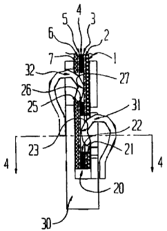
With reference to Figures 1 to 3 there is shown a first embodiment of an
electrochemical sensor. The sensor comprises a polyester spacer 4
approximately 25 mm x
5 mm and 100 microns thick and having a circular aperture 8 of 3.4 mm
diameter.
CA 02284634 1999-09-20
WO 98/43073 PCT/AU98/00184
-5-
Aperture 8 defines a cylindrical cell wall 10. Adhered to one side of spacer 4
is a first
insulating substrate polyester sheet 1 having a first coating of palladium 2.
The palladium
was sputter coated on sheet 1 at between 4 and 5 millibar pressure in an
atmosphere of
argon gas to give a uniform coating thickness of about 100-1000 angstroms.
Sheet 1 is
adhered by means of adhesive 3 to spacer 4 with palladium coating 2 adjacent
spacer 4 and
covering one side of aperture 8.
A second insulating substrate 7 consists of a polyester sheet having a second
sputter
coating 6 of palladium adhered by means of contact adhesive 5 to the other
side of spacer 4
and covering the opposite side of aperture 8. There is thereby defined a cell
having
to cylindrical side wall 10 and closed at one cylinder end by a first
electrode of palladium
metal 2. The other cylinder end wall is a second electrode formed from
palladium 6. The
assembly is notched at 9 to provide a means for admission of a solution to the
cell, and to
allow air to escape.
Adjacent one end 20 a cut-out aperture 21 pierces first insulating layer 1 and
first
~ 5 metal layer 2. In the present example cut-out 21 is oval-shaped. A
cowesponding cut-out
portion 22 in spacer 4 is in registration with cut-out 21. Figure 3 shows a
side elevation
cross-section of sensor 1 inserted into a receiving slot formed in pan 30 of
measuring
apparatus and to which is mounted a first resilient contactor 31 and a second
resilient
contactor 32. Upon insertion of sensor end 20 into the slot, contactor 31
rides over the
20 outer surface of insulating layer 1 and clicks into the well formed by
apertures 21 and 22 to
engage a first contact area portion 23 of metal layer 6. First contact area 23
is a portion of
the same metal layer 6 deposited on insulating layer 7 from which the second
electrode is
formed and is therefore in electrically conductive communication with the
second electrode
CA 02284634 1999-09-20
WO 98/43073 PCT/AU98/00184
-6-
area of cell 8. Contact area 23 is in effect defined by the diameter of cut-
out 20 of spacer 4
in the present example.
In the embodiment shown in Figure 1 a second circular cut-out portion 25
spaced
further from edge 20 than aperture 21 extends through second insulating layer
7 and second
metal layer 6. A cut-out portion 26 (see Figure 2) of spacer 4 corresponds
with and
registers with cut-out portion 25 of insulating layer 7. Referring again to
Figure 3, in use
the sensor is configured to permit a second resiliently biased contactor 32 to
extend
through the well defined by cut-out portions 25 and 26 whereby resilient
contactor 32
engages and makes electrical contact with metal layer 2 at 27 and thereby with
the first
t o electrode 2 of cell 8.
Resilient connectors 31 and 32 are arranged in a slot 30 of the measuring
device and
are electrically connected in a measuring circuit. In use, the sensor is
inserted into slot 30
with edge 20 leading. The first resilient contactor 31 rides over the end
margin of the
sensor 1 until it encounters first aperture 21,22 whereupon it click engages
with the
opening and makes electrical contact with the first contact area 23 of metal
layer 6. Slight
additional insertion of sensor 1 in slot 30 causes the second contactor 32 to
click engage
with the second aperture 25, 26 and make contact with second contact area 27
of metal
layer 2.
Spacer 4 surrounds both apertures and ensures that, despite the intrinsic
flexibility of
2o the insulating layers and the thinness of the sensor, electrical contact
can be made with
reliable precision.
A second embodiment of the invention is shown in Figures 5, 6 and 7 wherein
parts
corresponding in function to corresponding parts of the embodiment of Figures
1 and 2 are
identified by corresponding numerals. The major difference between the second
CA 02284634 1999-09-20
WO 98/43073 PCT/AU98/00184
embodiment and the first is that in the second embodiment cut-out portions 21,
22 are cut
from one side edge of sensor l while cut-out portions 25, 26 are cut out from
the opposite
side edge of the sensor 1. In this case contactors 31 and 32 are spaced
laterally and click
substantially simultaneously into their respective cut-out opening. The cut-
out openings
are surrounded on three sides by spacer 4, the fourth side being exposed at
respective edges
of the sensor.
Although in the embodiment shown in Figures 5, 6 and 7 the openings are at a
corresponding distance from end 20 in other embodiments they could be spaced
in the
longitudinal direction as is the case in the first described embodiment. This
ensures that
contact is only made when the sensor is inserted in a cprrect orientation and
ensures correct
polarity.
A third embodiment is shown schematically in Figure 8. In this case the
openings
take the form of slots 21, 25 extending longitudinally from edge 20. For
preference spacer
4 extends around all edges of openings 21 and 25 of Figure 8 but in a less
preferred
embodiment spacer 4 only extends on three sides of slots 21 and 25 in which
case click
engagement is not obtained or is obtained only if the contacts extend from the
opposite
direction. However the advantage that the contact pad area of the sensor is at
a
predetermined dimension from the opposite face is maintained. If desired the
slots can
differ in length and co-operation with contacts spaced longitudinally so that
contact with
2o both contacts requires correctly orientated insertion of the sensor.
It will be understood that both construction materials and dimensions are
given
merely by way of example and that sensors of a differing design or
construction may utilise
the invention. One, two or more than two contacts may be provided by the means
shown.
The invention extends to include a power source or measuring device when
connected to a
CA 02284634 1999-09-20
WO 98/43073 PCT/AU98/00184
_g_
sensor by the means described. Any suitable form of contactor may be used with
sensors
according to the invention.