Note: Descriptions are shown in the official language in which they were submitted.
CA 02285236 1999-09-30
WO 98/49771 PCT/US98/06870
BATTERY LIFE EXTENDING TECHNIQUE FOR
- MOBILE WIRELESS APPLICATIONS
10
FIELD OF THE INV~ r~N
This invention relates to wireless transmitters
and, in particular, to a technique for extending the
battery life in such a transmitter.
BACKGROUND
Extending battery life is a key concern for users
and manufacturers of cellular telephones and other
portable transceivers. A powerful signal generated and
transmitted by the wireless transceiver draws more
power from the battery than when a lower power signal
is generated and transmitted. Accordingly, a number of
prior art techniques have been employed to adjust the
gain of a portable transmitter so as to not transmit a
signal more powerful than necessary for adequate
communications. Examples of such ways of automatically
adjusting the output power level of a transmitter are
described in U.S. Patent Nos. 4,760,347, 5,/29,098, and
5,446,756, incorporated herein by reference.
Although the prior art techniques selectively
reduce the output power of the transmitter, the
efficiency of the transmitter is not improved by the
prior art methods. The transmitter is typically
biased, and operating voltages are set, so that the
transmitter output signal will not distort in an
adverse way at the highest expected output signals.
These worse case operating conditions can draw
_Z_
CA 02285236 1999-09-30
WO 98/49771 PCT/US98/06870
significant power from the battery even when no signal
is being transmitted. Such worst case operating
conditions are not required when the transmitter is not
transmitting its maximum signal. Hence, the
S transmitter's efficiency is lower when transmitting
lower power output signals. A lower efficiency equates
to wasting battery power, reducing talk time.
what is needed is a technique for extending the
battery life in mobile wireless applications.
SUN~IARy
A technique is described herein which dynamically
reduces the operating voltage applied to a
transmitter's power amplifier in a mobile wireless
transceiver so as to increase the efficiency of the
transmitter when the transmitter is not outputting its
maximum output power. Thus, the total power
consumption of the transmitter is reduced as compared
to prior art transmitters. In another embodiment, the
bias voltage or bias current levels within the
transmitter are also varied to optimize the efficiency
of the transmitter at a particular output power level.
This technique of controlling the transmitter's
operating voltage and bias voltage/current may be used
in conjunction with conventional techniques for
automatically reducing the gain of the transmitter.
In a preferred embodiment, a highly efficient
switching regulator is controlled by a control circuit
to adjust the operating voltage and bias
voltage/current for the power amplifier in the
transmitter. The control circuit has as its input any
of a variety of signals which reflect the actual output
of the transmitter or the desired output power of the
transmitter.
-2-
~ ~ ".
CA 02285236 1999-09-30
WO 98!49771 PCT/US98/06870
BRIEF DESCRIPTION OF THE DRAWINGS
Fig. 1 is a block diagram of the basic components
of a transmitter section in a wireless transceiver
incorporating one embodiment of the present invention.
. 5 Figs. 2-6 illustrate various embodiments of
controllers for controlling an output of a voltage
regulator for application to a power amplifier in a
wireless transceiver.
Fig. 7 illustrates one embodiment of a controller
for controlling an output voltage of a voltage
regulator for application to a receiver in a wireless
transceiver.
Figs. 8 and 9 illustrate a conventional buck type
regulator and a boost type regulator, respectively.
Fig. 10 illustrates one embodiment of a power
amplifier which has its efficiency improved using the
present invention.
DETAILED DESCRIPTION OF THE PREFERRED EMBODIMENTS
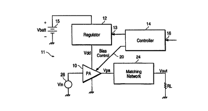
Fig. 1 illustrates a power amplifier 10 for a
transmitter 11 whose operating voltage Vdd is provided
by a variable voltage regulator 12. The output voltage
Vdd of regulator 12 is controlled by a signal from a
controller 14 applied to a control terminal 13. A
battery 15 supplies power to regulator 12.
Controller 14 receives a signal at an input
terminal 16 which signifies the actual output power of
the power amplifier 10, the desired output power of
amplifier 10, or a measure of the output voltage swing
of amplifier 10. Controller 14 then sets, based on
this input signal, the output voltage Vdd of regulator
' 12 such that amplifier 10 will operate under its most
efficient conditions for the particular output power
' level.
Controller 14 also, optionally, provides a bias
voltage or bias current control signal to amplifier 10
-3-
CA 02285236 1999-09-30
WO 98/49771 PCT/US98/06870
via line 20 to adjust the bias current or voltage
levels in amplifier l0 for optimum efficiency at a
particular output power level.
When amplifier 10 is outputting its maximum power
S level, the output voltage Vpa swing of amplifier 10 is
a maximum, and amplifier 10 operates with relatively
high efficiency. The various transistors and other
components in amplifier 10 are biased and otherwise
operated so as not to introduce significant distortion
into the output signal. As the output power is
reduced, the output voltage swing and current drawn
from battery 15 are reduced. In accordance with one
embodiment of the invention, because of the reduced
output voltage swing, the operating voltage Vdd
provided to amplifier 10 by regulator 12 is reduced,
without introducing distortion, to save additional '
power.
Further, in accordance with one embodiment of the
invention, as the power output level is reduced, the
bias voltages and currents are also reduced, without
introducing distortion, to save additional power.
Power consumption is the product of the RMS
voltage and current drawn from battery 15. Hence, by
reducing the RMS voltage to amplifier 10, power
consumption is reduced beyond that provided by prior
art power consumption techniques. Because cellular
telephones generally operate at less than full power
most of time, using the invention shown in Fig. 1 will
extend the life of battery 15 significantly.
A matching network 24 (e. g., a resonant circuit)
interfaces the output of amplifier 10 to a load RL.
Luad RL may be an antenna or other load. An input
signal generator 26 generates a modulated RF signal Vin
in a conventional way and may include automatic gain
control circuitry.
-4-
_~.~.~_~_-_.,..~,.w.w_ _, .~ ~._~.. . ~. r...
CA 02285236 1999-09-30
WO 98/49771 PCT/US98106870
Figs. 2-6 illustrate some of the techniques which
may be used by controller 14 to detect the output power
or desired output power of amplifier 10 in order to
suitably control regulator 12 to generate a variable
Vdd for amplifier 10 or to control the bias settings in
amplifier 10.
In Fig. 2, a power detector 30 is connected to the
output of power amplifier 10 or to the output of the
matching network 24, via a coupler 31, to generate a
voltage at lead 32 related to the output power of
amplifier 10. Coupler 31 couples a small percentage of
the output signal to the power detector 30. Power
detectors are well known and may take many forms.
Controller 42 converts the signal on lead 32 into a
control signal for regulator 12 for adjusting Vdd to
optimize the efficiency of amplifier 10.
Controller 42 may be coupled to a feedback
terminal 43 of regulator 12, where the feedback signal
Vfb has a predetermined relationship with the voltage
on lead 32. Thus, controller 42 may simply be a level
shifter or suitable amplifier. By appropriate design
of the power detector 30, the feedback terminal 43 of
regulator 12 may instead be directly connected to
lead 32, so that the power detector 30 acts as the
controller. The relationship between the input of
controller 42 and the output of controller 42 is to be
determined based upon the particular regulator 12 and
power amplifier 10 used.
Some cellular telephones and other wireless
3o transceivers already employ an output power detector
for another purpose, and, thus, the present invention
' may be easily incorporated into such devices.
Regulator 12 may be any conventional high-
' efficiency switching regulator which provides an output
voltage based upon a feedback signal, as is well-known
in the art. In conventional voltage regulator
-5-
CA 02285236 1999-09-30
WO 98/49771 PCT/US98/06870
circuits, the feedback terminal of a regulator is
connected to a divided regulated output voltage.
Fig. 3 illustrates a controller 50 which senses
the output voltage Vpa of amplifier 10 and essentially
acts as a negative peak detector to output a voltage
Vnp representative of the most negative output of
amplifier 10 over a period of time. The battery
voltage Vbatt applied to terminal 52 slowly pulls up
node 54 to the battery voltage through resistor 56.
Voltages applied to the cathode of diode 58 which are
lower than one diode drop below the voltage at node 54
pull down the voltage at node 54 to approximately the
most negative voltage applied to terminal 52 plus~a
diode drop. The selection of the resistor 56 value and
the capacitor 59 value determines the response of
controller 50. The RC time constant is preferably set
so that there is no appreciable change at node 54 from
cycle to cycle.
The voltage at node 54 is applied to one input
terminal of an amplifier 60, and a reference voltage 62
is applied to another input terminal. The output of
amplifier 60 is applied to the feedback terminal of
regulator 12. In response, regulator 12 provides an
operating voltage Vdd to amplifier 10 so as to maintain
the voltage at node 54 at approximately Vref. If Vref
is held fixed, then controller 50 acts to regulate the
minimum voltage across the amplifier 10 output
transistors) needed to avoid adverse distortion, thus
optimizing the amplifier's efficiency at all output
power levels. The technique of Fig. 3 may be used to
control the minimum voltage across the transistors in
all stages of amplifier 10 (e.g., transistors Q1 and Q2
in Fig. 10). For example, with reference to Fig. 10,
the minimum drain-source voltage across transistors Q1
and Q2 to allow transistors Q1 and Q2 to operate in a
linear region is regulated using the circuit of Fig. 3.
-6-
._._.~._w- _ .__-.~_~_. . . , , .
CA 02285236 1999-09-30
WO 98!49771 PCT/US98/06870
A buffer may be needed between the output of amplifier
and the input of controller 50 to avoid undue
loading.-
Fig. 4 illustrates a controller 70 for regulator
. 5 12 which receives as its input a receive signal
strength indication (RSSI?, provided by a conventional
RSSI circuit 72 which generates a voltage indicating
the strength of a received signal. The strength of the
received signal is, in certain cases, indicative of the
10 required power to be transmitted for adequate two-way
communication. This is especially true when the remote
originating transmit power is known. The wireless
transceiver may already contain a RSSI circuit 72 for a
different purpose. A higher RSSI signal thus indicates
to controller 70 to provide a feedback signal to
regulator 12 to lower the voltage Vdd to amplifier 10
to improve the efficiency of amplifier 10 at the lower
output power.
Fig. 5 illustrates how an input into controller 76
may be the baseband signal 78 which is mixed with the
modulating RF carrier, generated by modulator 80, by
multiplier 82. Since the output power of amplifier l0
varies with the amplitude of the baseband signal ~78,
controller 76 may cause regulator 12 to modulate the
voltage Vdd into amplifier 10 in accordance with the
baseband signal. The technique of Fig. 5 is only
applicable for forms of modulation which have non-
constant envelopes.
In another embodiment, shown in Fig. 6, controller
83 receives its signal directly from the output of
amplifier 10 or the matching network 24. Controller 83
converts this signal level into a control signal for
regulator 12.
' Other forms of controllers would be suitable
depending upon the specific transmitter to be
controlled.
_7_
CA 02285236 1999-09-30
WO 98/49771 PCT/US98106870
Fig. 7 illustrates a receiver 85 in a wireless
transceiver which receives its operating voltage Vdd
from regulator 12. Controller 87 controls the output
of regulator 12 to improve the efficiency of receiver
S 85 at lower received signal levels. A lower strength
received signal, detected by RSSI circuit 72, lowers
the Vdd applied to receiver 85 to optimize efficiency.
Bias voltage/current levels may also be adjusted by
controller 8~ via line 88.
Figs. 8 and 9 illustrate two types of simple
switching regulators: Fig. 8 illustrates a buck type
regulator 90, and Fig. 9 illustrates a boost type
regulator 92. Such regulators may be used for
regulator 12 in the various figures. In such
regulators, the duty cycle of the switch S1 (typically
a switching transistor3 is controlled, where the duty
cycle is directly proportional to the output voltage
Vdd of the regulator. A duty cycle controller 94
controls the switching of S1 based upon a feedback
signal Vfb from any of the controllers shown in
Figs. 1-7. A reference voltage Vref is compared to the
feedback signal by amplifier 96 for adjusting the duty
cycle of switch S1. An oscillator 98 provides the
switching frequency of switch S1. Those skilled in the
art are familiar with the operations of the regulators
of Figs. 8 and 9. A boost-buck regulator may also be
used, which is typically a combination of the circuits
of Figs. 8 and 9.
Fig. 10 illustrates one of the many appropriate
types of power amplifiers 10 which may be used with the
present invention. A modulated RF input signal from
generator 26 is supplied through resistor R and
capacitor C1 to the input of a field effect transistor
Q1. A variable bias voltage generator 106, controlled
by controller 14 in Fig. 1, provides a bias voltage for
operating transistor Q1 around a certain operating
_g_
CA 02285236 1999-09-30
WO 98/49771 PCTIUS98/06870
point. Inductor L1 and capacitor C1 form an input
matching network for transistor Q1. The signal
generated at the drain of transistor Q1 is provided to
the gate of transistor Q2, via DC blocking capacitor
C2, for further amplification. Inductor L2, inductor
L3, and capacitor C2 farm a matching network between
transistors Q1 and Q2.
The drain of transistor Q2 provides the output Vpa
of amplifier 10. A second variable bias voltage
generator 108, controlled by controller l4 in Fig. 1,
provides a bias voltage for operating transistor Q2
around a certain operating point. The drain of
transistor Q2 is connected to a matching network 24 for
appropriate resonant tuning to improve gain, lower the
return loss, lower distortion, increase output power,
and increase efficiency. The matching network 24
consists of inductor L4 connected between Vdd2 and
transistor Q2, inductor L5, and capacitors C3 and C4.
The voltage output Vout is then applied across a load
RL (e. g., an antenna) for transmission.
The operating conditions of transistors Q1 and Q2
must be set so that the voltage swings and/or drain
currents of transistors Q1 and Q2 are not distorted in
an unacceptable way. The adjustable bias voltages
Vbiasl and Vbias2 as well as voltages Vddl and Vdd2 are
therefore dynamically controlled to avoid such
distortion of the signals provided by transistors Q1
and Q2. Suitably controlling the operating conditions
using the present invention results in less battery
power being wasted through the various conduction
paths.
The variable voltage sources (e. g., controllable
regulators) used for sources 106 and 108 may be
conventional. The particular bias voltages needed at
various output power levels are determined on a case-
-9-
CA 02285236 1999-09-30
WO 98149771 PCT/US98/06870
by-case basis depending upon the particular amplifier
and application.
The controller 14 tFig. 1) may control the output
of regulator 12 to set the Vddl and Vdd2 levels to be
the same or different, depending on the minimum voltage
needed to operate transistors Q1 and Q2 at low
distortion at a particular output power.
In the example shown in Fig. 10, transistors Q1
and Q2 are metal-semiconductor field effect transistors
(MESFETs).
A power amplifier using bipolar technology may
also utilize the present invention, where the
collector-emitter voltage Vce of the amplifier's
transistors) is regulated to be a minimum needed to
operate the transistors) at all output levels without
distortion. Such an amplifier may replace the MESFET
transistors Q1 and Q2 in Fig. l0 with bipolar
transistors. MOSFET transistors may also be used.
This technique of dynamically adjusting the
operating conditions in an amplifier may be applied to
many forms of power amplifiers, and the particular type
of controller used will depend upon the method which
will provide the most efficient use of battery power. at
a reasonable cost. Many of the circuits which generate
the input to controller 14 (Fig. 1) already exist in
certain cellular telephones, such as the power
detection circuit 30 of Fig. 2 and the RSSI circuit 72
of Fig. 4. The present invention is not restricted to
any particular switching regulator (e. g., PWM, PFM),
and a suitable regulator may also be a non-switching
regulator, such as a linear regulator. However,
switching regulators are known to be highly efficient.
It is expected that the present invention will
increase the battery life of cellular telephones and
other wireless transceivers by as much as SO% or more.
In some applications, it is anticipated that battery
-10-
CA 02285236 1999-09-30
WO 98/49771 PCT/US98/06870
life will be at least doubled using the present
invention.
while particular embodiments of the present
invention have been shown and described, it will be
S obvious to those skilled in the art that changes and
modifications may be made without departing from this
invention in its broader aspects and, therefore, the
appended claims are to encompass within their scone all
such changes and modifications as fall within the true
spirit and scope of this invention.
-11-