Note: Descriptions are shown in the official language in which they were submitted.
CA 02285612 1999-10-14
WO 99/21048 PCT/AU98/00868
1
COATED SUNGLASS LENS
The present invention relates to optical articles bearing a light absorbing
coating. -
The optical articles according to the present invention are preferably
employed in the preparation of articles such as optical lenses, including
spectacle
lenses, including sunglass lenses, visors, shields, glass sheets, protective
screens, and the like.
Sunglasses generally serve to attenuate transmitted sight, but aside from
the level of light transmittance, there ace other features that distinguish
different
sunglass lenses, such as material, transmitted colour, scratch resistance,
reduction of side glare, ultra-violet transmittance, cosmetic appearance etc.
Coatings may be applied to enhance the performance of sunglass lenses. Such
coatings might include scratch resistant coatings, hydrophobic coatings for
easier
cleaning, anti-reflection coatings on the concave surface for reducing side
glare or
"mirror' ~ (or "interference") coatings for producing fashionable fens
colours.
General purpose sunglass lenses should meet certain standard specifications,
including luminous transmittance, traffic signal recognition and UV
transmittance
(e.g. ANSI 280.1-1995).
In addition to their performance characteristics, sunglass lenses should be
simple and economical to produce in a reliable manner.
As is known in the prior art, the preferred method for producing sunglass
lenses is dependent on the material involved. In all cases a light-attenuating
material is either incorporated into the substrate material or applied over
its
surface in a process known as ~tintingn. For example, glass lenses are often
tinted
by introducing coloured additives to the molten glass, and similarly
polycarbonate
tenses are injection-moulded from pre-coloured plastic granules. A
disadvantage
associated with this method of production is that for economical reasons, very
large batches of coloured raw material must be purchased , limiting
flexibility in the
range of tint colours that can be offered in the sunglass lens product.
Moreover,
CA 02285612 1999-10-14
WO 99/21048 PCT/AU98/00868
2
prescription sunglass lenses with highly varying thickness will also exhibit
non-
uniform transmittance when coloured in this way. Hard resin lenses (another
commonly used ophthalmic plastic) are usually dipped in a hot, liquid dye
which is
imbibed into the plastic. This process also has disadvantages, such as
difficulty in
achieving tint uniformity, poor colour reproducibility and its requirement
that if the
lens has a scratch resistant coating, it must be semi-permeable to allow
imbibation
of the dye molecules, hence compromising the scratch resistance. If a
reflective
mirror coating is desired, the tinted substrate is then cleaned and coated in
an
evaporative box coater. Such mufti-stage processes are both time-consuming and
expensive.
One proposal in the prior art to overcome some of the problems associated
with lens tinting is to apply the light absorbing material as a thin film on
an
essentially transparent substrate. United States Patent No. 5,770,259 (Parker
and
Soane) describes a method for tinting sunglass lenses using a curable primer
7 5 containing a tinting agent. Vacuum deposition allows the light absorbing
coating to
be applied in a relatively fast, clean, flexible and controllable manner.
United
States Patent No. 5,729,323 (Arden and Cumbo) describes a sunglass formed by
depositing a multi-layer light absorbing coating containing TiOx (x=0.2-1.5)
on the
concave surface of the substrate. The coating is anti-reflective from the
wearer's
side of the lens. United States Patent No. 3679291 (Apfef and Gelber)
describes
a metal-dielectric multi-layer coating that is light absorbing and has an
asymmetric
reflectance, being anti-reflective from one side and with strong colour on the
other
side.
Another time-consuming step in the production of corrective sungiass
lenses is the surfacing of the lenses. Corrective (or prescription) sunglass
lenses
are often dispensed using "semi-finished blanks" - lenses that have a pre-
moulded
front surface and a back surface that must be ground and polished to satisfy
the
individual wearer's corrective prescription. For plastic tenses in particular,
tinting
and the deposition of further lens coatings must be performed after surfacing
the
lens, resulting in a long and labour-intensive process to produce and deliver
the
sunglass lenses. One means to simplify. and accelerate lens delivery is to
employ
CA 02285612 1999-10-14
WO 99/21048 PCT/AU98100868
3
a wafer lamination scheme, where front and back lens wafers spanning a large
range of optical powers are simply glued together to produce a lens of
virtually any
desired prescription. Instead of maintaining a complex optical qrindina any
polishing workshop, the optical dispenser need only maintain an inventory of
wafers and a lamination unit. The use of fast curing glues allows lenses to be
produced in only minutes. Additional performance enhancing coatings may be
applied to the wafers at the factory, so that the dispenser may provide the
desired
product features immediately, simply by selecting the appropriate wafers from
his
inventory.
For laminated lens wafer systems, for example of the Sola International
Matrix~-type, liquid bath tinting is not a desired option - it is a low yield
process
involving significant handling and possible distortion of fragile wafers. Such
tinted
lenses may also exhibit poor abrasion and scratch resistance and variable
depth
of colour.
Moreover, for sunglass lenses in particular, it would be a significant
advance in the art if, in addition, reflection of visible light at the concave
(or rear)
lens surface could be kept sufficiently low to avoid glare from incident light
at the
concave surface.
Accordingly, it is an object of the present invention to overcome, or at
least alleviate, one or more of the difficulties or deficiencies related to
the prior art.
Accordingly, in a first aspect of the present invention there is provided an
optical lens including
an optically clear lens element; and
a light absorbing coating on the front surface of the lens that
attenuates transmitted light;
has a coloured or colourless reflection as seen from the front of the
sungiass lens; and
is anti-reflective as seen from the eye side of the lens.
It will be understood that, in accordance with the present invention, one or
CA 02285612 1999-10-14
WO 99/21048 PCT/AU98/00868
4
more surfaces of an optical lens is coated with a light absorbing coating.
This light
absorbing coating may be applied to either the outside surface of the lens or
an
inside surface of a lens wafer (where it is protected from scratching once the
wafers are laminated) as discussed below. The light absorbing coating may
preferably serve three purposes at once - to attenuate transmitted light,
effectively '
providing the sungfass "tint," to produce a reflected colour that is of
pleasing
appearance and to reduce or minimise back reflections seen by a wearer of the
sunglass lenses.
In a preferred form, the light absorbing coating may function as a mirror
coating. Thus, the tinting and mirror coating processes may be combined into
one
with this coating.
Further the deposited coating may exhibit much improved adhesion and
this improved abrasion resistance.
In a further aspect of the present invention there is provided an optical
lens including
an optically clear lens element; and
a light absorbing coating on the rear surface of the lens, such that the light
absorbing coating
attenuates transmitted light;
has a coloured or colourless reflection as seen from the front of the
sunglass lens; and
is anti-reflective as seen from the eye side of the lens.
Preferably the tight absorbing coating is an asymmetric reflectance, light
absorbing coating including a plurality of overlapping light absorbing and
generally
transparent layers, and wherein the thickness and/or number of the respective
layers are selected to provide an anti-reflective effect on the eye side of
the optical
lens and a desired colour on the other side of the lens.
By the term ucoloured or colourless reflection", as used herein, we mean
that fight from a white fluorescent source is reflected from the surface of
the
CA 02285612 1999-10-14
WO 99/21048 PCT/AU98/00868
optical lens to an observer such that the reflected light is coloured or white
respectively.
By the term "asymmetric reflectance", as used herein, we mean that the
multi-layer coating renders the lens anti-reflective when viewed from one side
of
5 the coating and exhibits a selected colour or colourless reflection when
viewed
from the other side.
The optically clear lens element may be a sunglass lens, ophthalmic fens
element, visor or the like. A sungiass lens is preferred.
By the term "ophthalmic lens element", as used herein, we mean all forms
of individual refractive optical bodies employed in the ophthalmic arts,
including,
but not limited to, lenses, lens wafers and semi-finished lens blanks
requiring
further finishing to a particular patient's prescription.
Where the optically clear lens element is an ophthalmic lens element, the
ophthalmic tenses may be formed from a variety of different lens materials,
and
particularly from a number of different polymeric plastic resins. A common
ophthalmic lens material is diethylane glycol bis (allyl carbonate). Lens
materials
with higher refractive indices are now growing in popularity. One such
material is
a CR39 (PPG Industries). Other high index lens materials are based on acrylic
or
allyfic versions of bisphenols or alfyl phthalates and the like. Other
examples of
lens materials that may be suitable for use with the invention include other
acrylics, other allylics, styrenics, polycarbonates, vinylics, polyesters and
the like.
The light absorbing coating may be formed from overlapping light
absorbing and generally transparent layers, as discussed above. Desirably the
light absorbing coating is formed from alternating transpare_ rat and
absorbing
layers.
The number and/or thickness of the light absorbing and generally
transparent layers may be selected to provide an eye side anti-reflective
coating
utilising suitable computer software.
CA 02285612 1999-10-14
WO 99/21048 PCT/AU98/00868
6
The combination of fight absorbing and transparent layers may be
selected to provide a bright, coloured reflection when viewed from the front
of the
lens at the same time. A mirror type coating may be produced.
The transparent layers may be formed from any suitable optically clear
material. The transparent layers may be formed of a dielectric material.
Preferably
the dielectric layers may be formed from metal oxides, fluorides or nitrides.
Metal
oxides which may be used for forming transparent layers include one or more of
SiO, Si02, Zr02, AI203, TiO, Ti02, Ti203, Y203, Yb20s, MgO, Ta205, Ce02 and
Hf02. Fluorides which may be used include one or more of MgF2, AIF3, BaF2,
CaFZ, Na3AIF6, Taz05, and Na5A13F1,4. Suitable nitrides include Si3N4 and AIN.
A silica (Si02) material is preferred.
in a particularly preferred embodiment, the first deposited layer may be a
silica layer followed by alternating light absorbing and generally
transparent,
preferably silica, layers. The transparent dielectric layers may be
substantially
thicker i<han the light absorbing or metallic layers. The first layer may be
of
approximately 10 to 75 nm, preferably approximately 25 to 60 nm. This first
layer
may provide significant improvement in the abrasion resistance of the multi-
Payer
coating.
The generally transparent layers within the body of the light absorbing
coating may be relatively thick. The thicknesses may be such as to generate
interference effects which substantially cancel out internal reflections.
Thicknesses of for example from approximately 20 nm to 100 nm, preferably
approximately 25 nm to 85 nm may be used.
The light absorbing layers of the light absorbing coating may be formed
from any suitable material. Metals, metal oxides or nitrides may be used.
Desirably a metallic layer may be selected to provide a generally neutral,
e.g. grey transmission. Accordingly a silver-coloured metal, e.g. Niobium
(Nb),
Chromium (Cr), Tungsten (W), Tantalum (Ta), Tin (Sn), Palladium (Pd), Nickel
{Ni)
CA 02285612 1999-10-14
WO 99121048 PCT/AU98/00868
7
or Titanium (Ti) or mixtures thereof may be used.
The thickness of the fight absorbing layers is such as to attenuate
transmitted light. The light absorbing or metallic layers may generally be of
a
substantially reduced thickness relative to the transparent or dielectric
layers. For
example if the material used is Niobium, the light absorbing layers may be
from
approximately 1 nm to 10 nm, preferably approximately 2 nm to 5 nm in
thickness.
In a preferred form, the light absorbing coating may include a total of 4 to
12 alternating light absorbing-generally transparent Payers, preferably 6 to 8
alternating layers. An additional primer layer may be included, as discussed
above.
The resultant coating may exhibit a silver (colourless) mirror-type
appearance. Alternatively the light absorbing coating may be modified to
produce
a different colour coating. For example a metallic oxide, e.g. silica or
niobium
oxide coating may be applied. A combination of dielectric top coatings may be
applied., A silica top coat may be added to modify colour and additionally
enhance
abrasion resistance.
Accordingly in a preferred form, the light absorbing coating includes
alternating layers of a dielectric material and a metallic material;
the dielectric material being selected from one or more of SiO, Si02, Zr02,
AI203, TiO, Ti02, Ti203, Y203, Yb203, MgO, Ta205, Ce02 and Hf02, MgF2, AIF3,
BaF2, CaF2, Na3AIF6, Ta205 and Na5A13F1~4; and Si3N4 and AIN; and
the metallic material is selected from the metals, metal oxides or nitrides
of one or more of Niobium (Nb}, Chromium (Cr), Tungsten (W), Tantalum (Ta),
Tin
(Sn), Palladium (Pd), Nickel (Ni) or Titanium (Ti).
More preferably the fight absorbing coating includes alternating layers of
silica (Si02) and chromium metal.
More preferably the light absorbing coating includes an additional titanium
dioxide layer or layers of such a thickness to provide a desired colour to the
CA 02285612 1999-10-14
WO 99/21048 PCT/AU98/00868
8
optical lens.
Alternatively, the light absorbing coating includes alternating layers of
silica and niobium metal.
Preferably the light absorbing coating includes an additional niobium
oxide (Nb2p5) and/or silica (Si02) layer of such thicknesses to provide a
desired
colour to the optical lens.
In a still further preferred embodiment the light absorbing coating further
includes compatible dielectric layers of suitable thickness to provide a
desired
colour to the optical lens.
The optical lens may further include one or more additional coatings.
Accordingly in a further aspect of the present invention there is provided a
multi-coated optical lens including
an optical article; and
a light-absorbing coating deposited on at least one surface of the optically
i 5 clear article; the light-absorbing coating including a plurality of
overlapping light
absorbing and generally transparent layers, and wherein the thickness and/or
number of the respective layers being selected to provide an anti-reflective
effect
on the eye side of the optical lens and a desired colour on the other side of
the
optical lens, and
an optically clear secondary coating which provides a desirable optical
and/or mechanical property to the optical article.
The optically clear secondary coating may preferably underlay or overlay
the light absorbing coating.
The secondary coating may be of any suitable type. The secondary
coating may be one or more of an anti-reflective, abrasion resistant, or
impact-
resistant coating. An abrasion-resistant coating is preferred. The combination
of
an abrasion resistant coating and an anti-reflective coating is particularly
CA 02285612 1999-10-14
WO 99/21048 PCT/AU98/00868
9
preferred.
An abrasion-resistant (hard) coating including an organosificone resin is
preferred. A typical organosilicone resin that is suitable for use in the
present
invention has a composition comprising one or more of the following:
1 ) organosiiane compounds with functional and/or non-functional groups
such as glycidoxypropyl trimethoxy silane;
2) co-reactants for functional groups of functional organosilanes, such as
organic epoxies, amines, organic acids, organic anhydrides, imines,
amides, ketamines, acrylics, and isocyanates; colloidal silica, sols and/or
metal and non-metal oxide sols; catalysts for silanol condensation, such
as dibutylin dilaurate;
3) solvents such as water, afcohols, and ketones;
4) other additives, such as fillers.
Abrasion resistant coats of acrylic, urethane, melamine, and the like may
also be used. These materials, however, frequently do not have the good
abrasion resistant properties of organo-silicone hard coatings.
The abrasion-resistant {hard) coating may be coated by conventional
methods such as dip coating, spray coating, spin coating, flow coating and the
like
or by newer methods such as Plasma Enhanced Chemical Vapour Deposition.
Coating thicknesses of between approximately 0.5 and 10 microns are preferred
for abrasion and other properties.
The secondary abrasion resistant coating may be applied to the front
and/or rear lens surfaces. The abrasion resistant coating may be of the type
described in United States Patent 4,954,591 to the Applicants, the entire
disclosure of which is incorporated herein by reference.
in a preferred aspect, one or both surfaces of the optical article may be
subjected to a surface treatment to improve bondabiiity and/or compatibility
of the
light absorbing and/or secondary coating. The surface treatment may be
selected
from one or more of the group consisting of plasma discharge, corona
discharge,
CA 02285612 1999-10-14
WO 99/Z1048 PC'T/AU98/00868
glow discharge, ionising radiation, UV radiation, flame treatment and laser,
preferably excimer laser treatment. A plasma discharge treatment is preferred.
The surface treatment, alternatively or in addition, may include incorporating
'
another bonding layer, for example a layer including a metal or metal compound
5 selected from the group consisting of one or more of Chromium, Nickel, Tin,
Palladium, Silicon, and/or oxides thereof.
The optical article may be a sungiass lens of the wrap-around or visor
type, for example of the type described in International Patent Application
PCT/AU97/00188 "improved Single Vision Lens" to Applicants, the entire
10 disclosure of which is incorporated herein by reference.
In a further aspect of the present invention, there is provided a method for
preparing an optical lens, which method includes
providing
an optically clear lens element; and
a light absorbing coating on the front surface of the lens that
attenuates transmitted sight;
has a coloured or colourless reflection as seen from the front
of the sunglass lens; and
is anti-reflective as seen from the eye side of the lens; and
depositing the light absorbing coating on a surface of the optical lens
element.
According to the present invention it has been found that, following the
method mentioned above, it is possible to achieve a relatively thin, light
absorbing
coating with consequent advantages in both optical and mechanical properties.
Preferably the method further includes
providing
an optically clear lens element,
a light absorbing material, and
a generally transparent material;
depositing overlapping layers of light absorbing material and generally
CA 02285612 1999-10-14
WO 99/21048 PC'T/AU98/00868
11
transparent material on a surface of the optical lens element, the number
and/or
thickness of the respective layers being selected to provide a desired colour
to the
front surface of the optical fens and an anti-reflective effect on the eye
side of the
optical lens.
In a preferred aspect the light absorbing or metallic material and generally
transparent or dielectric material, preferably Nb and SiO~ or Cr and SiO~, are
deposited as alternating layers.
The deposition step may be a vacuum deposition step. The deposition
step may be conducted in a coating apparatus. A box coater or sputter coater
may be used.
The light absorbing coating may preferably be formed on the surfaces of
the substrate according to the process and the box coaters as described in the
itziian Patent No. 1.244.374 the entire disclosure of which is incorporated
herein
by reference.
In accordance with said method, the various layers of the light absorbing
coating may be deposited in subsquent steps utilising a vacuum evaporation
technique and exposing the growing layers to a bombardment of a beam of ions
of
inert gas.
Moreover, in accordance with the preferred method, the deposition of the
layers may be achieved at a low temperature (generally below 80°C),
using an ion
beam having a medium intensity (meaning the average number of ions that reach
the substrate) included beween approximately 30 and 100 uA/cm2 and the energy
included between approximately 50 and 100 eV.
Preferably, the optical article is maintained at an elevated temperature
during the deposition of the various layers of the light absorbing coating.
More preferably the optically clear lens element includes
a front lens wafer including
CA 02285612 1999-10-14
WO 99/21048 PCT/AU98/00868
12
a contact surface,
a complementary back lens wafer, including
a contact surface
and the overlapping layers of light absorbing material and generally
transparent material are deposited on a surface of the front andJor
complementary
back lens wafer.
A laminate adhesive may be applied to one or both contact surfaces. the
front lens wafer and back lens wafer being brought into contact and the
laminate
so formed being subjected to a curing step to form a laminate optical lens.
In a further preferred aspect of the present invention, there is provided an
optical lens element including
a lens wafer having
a first lens surface; and
a second lens surface,
the first or second surface having deposited thereon
a light absorbing coating that
attenuates transmitted light;
has a coloured or colourless reflection as seen from the front of the
sungiass lens; and
is anti-reflective as seen from the eye side of the lens.
Preferably the light absorbing coating is an asymmetric reflectance light
absorbing coating including a plurality of overlapping fight absorbing and
generally
transparent layers; the thickness and/or number of the respective layers being
selected to provide a desired colour to the optical lens element and an anti-
reflective effect on the eye side of the lens element after lamination of the
tens
wafer.
The coated lens wafer may be a front surface wafer or a rear surface
wafer. Where the coated lens wafer is a front surface wafer the light
absorbing
coating may be deposited on the first (front) or second (rear) lens surface
thereof.
CA 02285612 1999-10-14
WO 99121048 PCT/AU98/00868
13
Where the coated lens wafer is a rear surface wafer, the light absorbing
coating is preferably deposited on the first (front) surface thereof.
Accordingly in a still further aspect of the present invention, there is
provided a laminate optical lens including
a front lens wafer including
a contact surface;
a complementary back lens wafer including
a contact surface; and
a light absorbing coating deposited on a contact surface, which light
7 0 absorbing coating
attenuates transmitted light;
has a coloured or colourless reflection as seen from the front of the
sunglass lens; and
is anti-reflective as seen from the eye side of the lens.
Preferably the light absorbing coating includes a plurality of overlapping
light absorbing and generally transparent layers; the thickness and/or number
of
the respective layers being selected to provide a desired colour to the
laminate
optical lens and an , anti-reflective effect on the eye side of the laminate
optical
lens, as discussed above.
It will be understood that, in this embodiment, in addition to the
advantages of the present invention described above, the light absorbing
coating
provided may be protected by the optical lens wafers themselves and is thus
virtually indestructible.
In addition, abrasion resistant and like coatings of the type described
above may be applied to the external surfaces of the laminate optical article.
The laminate optical article may be fabricated in a manner similar to that
described in International Patent Application PCT/AU9fi/00805, "Laminate
Article",
to Applicants, the entire disclosure of which is incorporated herein by
reference.
CA 02285612 1999-10-14
WO 99/21048 PC'T/AU98100868
14
Where the light absorbing coating is applied inside the laminate, particularly
for hard resin lenses, because the lens is not tinted in a liquid bath, the
scratch
resistant coating applied to the exterior of the wafers does not need to be
semi-
permeabie (to allow passage of the tint molecules through to the substrate).
Therefore, the most durable, non-tintable scratch resistant coatings may be
applied and the final product is extremely durable. The light absorbing
coating is
protected inside the laminate and cannot be scratched. Eecause the light
absorbing coating is located approximately in the centre of the laminate, when
the
lens is edged for mounting into spectacle frames, the edges appear "dark" and
it is
difficult to discern that the "tinted" appearance of the lens is due only to a
very thin
coating. Finally, as can be seen in Figure 2 below, there is a double
reflection
from the front of the lens, one 'white" reflection from the front of the front
wafer
and one coloured reflection from the light absorbing coating inside the
laminate. If
the front wafer is thin and has no optical power, the twc reflections overlay
one
another and only a single reflection is observed. However, if the front wafer
is
thick and has surfaces of different curvature, then the two front reflections
become
apparent. A quite pleasing "glossy" effect is obtained.
Before the lens wafers of the laminate lens are bonded, they may be too
thin to meet United States F.D.A impact requirements. A sunglass wearer may be
put at risk if he wears sunglasses which have been made using only the front
or
back wafer of the laminate. It may be necessary for a prescription sunglass
manufacturer to ensure that non-laminated wafers are not mounted in sunglass
frames for general use. One way to achieve this end is to ensure that the lens
wafers are visibly identified with a warning symbol as unsuitable for use, in
such a
way that after the wafers are laminated, the warning is no longer visible. For
example, the current Matrix~ lens lamination system includes a warning symbol
in
the centre of the contact surface of each lens wafer - a roughened area of the
surface that causes unacceptable disturbance of the wearer's vision and thus
effectively prevents use of non-laminated wafers alone in spectacles. However,
when the wafers are laminated using an adhesive of refractive index suitably
matched to the lens material, the interface corresponding to the roughened
surfaces optically disappears, so that the warning symbol is no longer
visible.
CA 02285612 1999-10-14
WO 99/Z1048 PCT/AU98/00868
If the light absorbing coating is applied over such a roughened contact
surface, it is visible from the front of the wafer. It is also visible from
the back of
the wafer, because until the water is laminated, it is exposed to air rather
than
another lens wafer, so the coating does not perfom~ antirefiectively as
designed.
5 The roughened surface causes substantial light scattering toward the wearer
and
significantly disturbs his vision, so much so that the front lens wafer would
not
conceivably be used in a non-laminated state as a sunglass lens. After
lamination, the coating is antireflective when viewed from the rear - light
scattering
from the roughened surface is very weak and so the roughened area is invisible
to
10 the wearer. If the contact surface of the lens wafer is roughened in a
cosmetically
pleasing fashion, then not only are non laminated lens wafers clearly
identified,
but after the coated wafers are laminated, a logo that is visible from the
front of
the lens but yet does not disturb the wearer's vision results.
Accordingly, in a preferred embodiment of the present invention a contact
15 surface of the front and/or back lens wafer bears a mark thereon, the mark
being
substantially visible from both sides of the wafer before lamination, but
which
becomes substantially invisible from the eye side of the finished laminate
lens.
Preferably the mark on the contact surface is visible from the front c~f the
laminated lens.
In an alternative embodiment where the mark on the contact surface is not
visible from the front of the final laminated lens, the light absorbing
coating
includes a silica top layer, the silica top layer bearing a mark visible prior
to
lamination, as discussed above.
Preferably the visible mark is rendered substantially invisible when the lens
wafer is contacted with a Laminate adhesive having a refractive index
approximately equal to that of the silica layer.
The light absorbing coating may for example be purposefully constructed to
have a top layer of silica, which has a refractive index of approximately
n=1.47.
An excimer laser or other etching technique can be applied to remove (or
merely
reduce the thickness of) the top silica layer of part of the coating in the
form of a
CA 02285612 1999-10-14
WO 99/21048 PCT/AU98I00868
16
warning label, which will be very visible before the wafer is laminated.
However,
after lamination, glue will fill the depressions caused by the etching, and
because
the glue can be chosen to have a refractive index very close to that of
silica, the
etched markings will have no optical effect and hence disappear, making the
laminated lens suitable for use.
Alternatively, instead of removing part of the top silica layer, a warning
label
may be deposited on top of the silica layer with a suitably index-matched
material,
for example an adhesive or polymer material. Again, after lamination, glue
will fill
the void around the raised warning label, and because the glue can be chosen
to
have a refractive index very close to that of silica and the label itself, the
warning
marking will have no optical effect and hence disappear, making the laminated
lens suitable for use.
Further characteristics and advantages of the present invention wilt be
apparent from the following description of drawings and examples of
embodiments of the present invention, given as indicative but not restrictive.
In the figures:
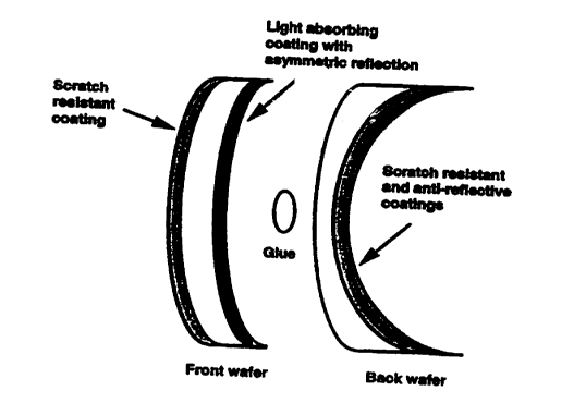
Figure 1 illustrates an embodiment of a sunglass lens according to the
present invention with the tight absorbing coating inside the laminate.
Figure 2 illustrates the attenuation of transmitted light through the
sunglass lens of Figure 1 from a forward light source.
Figure 3 illustrates the attenuation of reflected light from the sungfass lens
of Figure 1 from side glare.
Figure 4 illustrates the transmission spectra of a "black" laminated lens
(see Table 1 ), as compared to a typical liquid-dye tinted hard resin sunglass
lens.
Figure 5 illustrates an embodiment of a laminated sunglass lens with
semi-visible internal markings.
CA 02285612 1999-10-14
WO 99/21048 PCT/AU98/00868
17
Figure 6 illustrates an embodiment of a sunglass lens according to the
present invention with the light absorbing coating on the outside surface of
the
front wafer.
Figure 7 illustrates the attenuation of transmitted light through the
sunglass lens of Figure 6 from a forward light source.
Figure 8 illustrates the attenuation of reflected light from the sunglass lens
of Figure 6 from side glare.
Figure 9 illustrates an embodiment of a sunglass lens according to the
present invention with the light absorbing coating on the outside surface of
the
back wafer.
Figure 10 illustrates the attenuation of transmitted fight through the
sungfass lens of Figura 9 from a forward light source.
Figure 11 illustrates the attenuation of reflected light from the sunglass
lens of Figure 8 from side glare.
EXAMPLE 1
Light absorbing coating on the inside of a laminated lens
Figure 1 shows a preferred embodiment of a tinted optical lens according to
the present invention. The front and back lens wafers are hard resin plastic
wafers from a commercial ophthalmic lens system (Sola International Matrix~
system). The back lens wafer is supplied with its external surface pre-coated
with
a scratch resistant and anti-reflective coating. The external surtace of the
front
wafer is also treated with a scratch resistant coating. The internal surfaces
of both
wafers are of uncoated hard resin.
A light absorbing coating with asymmetric reflectance is applied to the
interface surface of the front wafer. (It may equally well be applied to the
internal
CA 02285612 1999-10-14
WO 99/21048 PCT/AU98/00868
18
surface of the back wafer instead. Only the first case will be discussed for
simplicity.) The coating is designed so that when the wafers are laminated,
neutral attenuation of transmitted light, an aesthetically pleasing colour
when
viewed from the front of the lens and anti-reflection from the wearer-side of
the
fens result, as shown in Figures 2 and 3. Referring to Figure 3, it will be
appreciated that possible reflections from surfaces behind the light absorbing
coating do not contribute in any significant manner, because their intensity
is
severely reduced by the incident light having initially passed through the
light
absorbing coating. Such reflections are therefore not indicated in the figure.
The mufti-layer light absorbing coatings consist of layers of absorbing
materials and transparent dielectrics. The layers of absorbing material
provide the
attenuation of transmitted light. The degree of attenuation is controlled by
adjusting the total thickness of these layers. If the absorbing material has a
neutral transmission spectrum (as do many metals), the transmission of the
coating will also be neutral, which is highly desirable for a sunglass lens
that does
net distort colour vision. By appropriately selecting the thicknesses of the
various
layers (which today is commonly achieved with the aid of computer software
packages), the reflectance of the coating may be designed to have the required
properties of a pleasing colour when viewed from the front of the lens and
anti
reflection from the wearer side.
CA 02285612 1999-10-14
WO 99/21048 PCT/AU98/00868
19
Table 7 lists the materials and layer thicknesses used in three differently
coloured embodiments of the light absorbing coating. The coatings were
deposited using a commercial evaporative box coater (Satis 1200).
TABLE 1
Layers Thickness
(nm)
Number Naterial Primary function Bronze Blue Black
Substrate
1 Cr Adhesion to substrate0.5 0.5 0.5
2 Ti02 Front colour 37 35 20
3 Si02 Front colour 9 50 20
4 Ti02 Front colour 88 _ 20
Cr Absorption 14 12 i 2
6 Si02 Back AR 65 65 65
7 Cr Absorption g g
8 Si02 Back AR 85 85 85
9 Cr Absorption 2.5 2.5 2.5
Si02 Scratch resistance 5 5 5
5 Table 1. Composition of three differently coloured embodiments of the (fight
absorbing coating as deposited inside the laminated sunglass lens.
The sequence of layers is relative to a light ray entering the front surface
of
the optical lens.
CA 02285612 1999-10-14
WO 99/21048 PCT/AU98/00868
Table 2 shows the optical performance of the sunglass lenses in
transmittance.
TAB LE 2
Transmission Bronze Blue Black
Luminous transmittance 12.1 11.4 13,5
{%)
CIE x coordinate (illum. 0.36 0.38 0.37
C)
CIE y coordinate (illum. 0.35 0.37 0.35
C)
Av. UVB transmittance 0 0 0
(%)
Av. UVA transmittance 1.8 1.4 2.2
(%)
Red traffic signal traps.16.3 16.3 18.1
(%)
Yellow traffic signal 13.6 13.3 15.3
traps. (%)
Green traffic signal traps.11.1 10.1 12.3
{%)
ANSI Standard 280.3 - yes yes yes
1997
Table 2. Optical performance of the sunglass lenses in transmission.
5 As shown in Figure 4, where the transmission spectrum of the bfack-
coloured sunglass lens is compared to a hard resin sunglass lens tinted by the
traditional liquid dye tinting process, the light absorbing coating has a
quite neutral
transmission, which provides excellent colour vision.
CA 02285612 1999-10-14
WO 99/21048 PC'T/AU98/00868
21
Table 3 shows the reflectance characteristics of the laminated sunglass
lenses. As seen from the wearer-side reflectances, the sungfass lenses are
indeed quite anti-reflective of side glare.
TABLE 3
Sungiass lens reflectance Bronze Blue B
Front side
Luminous reflectance (%) 8.6 15.8 4.5
CIE coordinate (illuminant0.36 0.23 0.26
C), x
C1E coordinate (illuminant0.35 0.23 0.24
C), y
Wearer side
Luminous reflectance (%) 0.9 1.0 1.1
CIE coordinate (illuminant0.30 0.25 0.26
C), x
C1E coordinate (illuminant0.31 0.24 0.29
C), y
Table 3. Optical performance of the sunglass lenses in reflection.
EXAMPLE 2
In the embodiment of the present invention illustrated in Example 1 (with
the light absorbing coating inside the laminate), it is possible to produce
semi-
visibfe markings or logos on the sunglass lenses, as shown in Figure 5. By
artificially roughening the surface of the wafer on the interface surface
underneath
the light absorbing coating (for example by etching the mould from which the
internal surface of the front wafer is cast in this case), patterns are
created and
embedded inside the lens after lamination. The roughened surface is visible
from
the front of the sungiass lens, because from this side of the fight absorbing
coating, the reflectance is non-negligible, so light is scattered from the
roughened
surtace. From the wearer side, because the coating is anti-reflective,
reflections
from the roughened surface are extremely weak, so that the markings are almost
impossible to see. Therefore the logo can even be placed in the optical centre
of
the lens without disturbing the wearer's vision.
CA 02285612 1999-10-14
WO 99/21048 PCT/AU98/00868
22
EXAMPLE 3
Light absorbing coating on the outside surface of the front wafer of a
laminated lens
Figure 6 shows another preferred embodiment of the sunglass lens. Again,
the front and back fens wafers are hard resin plastic wafers from a commercial
ophthalmic lens system (Sofa International Matrix~ system). The back wafer is
supplied with its external surface pre-coated with a scratch resistant and
anti
reflective coating. The external surface of the front wafer is also treated
with a
scratch resistant coating. The internal surfaces of both wafers are of
uncoated
hard resin.
In this embodiment, the light absorbing coating with asymmetric reflectance
is applied to the outside surface of the front wafer. Neutral attenuation of
transmitted light, an aesthetically pleasing colour when viewed from the front
of
the lens and anti-reflection from the wearer-side of the lens again result
after the
wafers xre laminated, as shown in Figures 7 and 8.
CA 02285612 1999-10-14
WO 99/21048 PCT/AU98/00868
23
Table 4 lists the materials and approximate layer thicknesses used in four
differently coloured embodiments of the light absorbing coating. The coatings
in
this case were deposited using a thin film sputter deposition system.
TABLE 4
Layers Thickness
(nm)
Number MaterialPrimary function SilverGold Blue Copper
Substrate
1 Si02 Scratch resistance50 50 50 50
2 Nb Absorption 2 2 2 2
3 Si02 Back AR 80 80 80 80
4 Nb Abso~tion 4 4 4 4
Si02 Back AR 80 80 65 fi5
6 Nb Absorption 4 4 4 4
Si02 Back AR 40 40 20 40
8 Nb Absorption 4 4 4 4
' Si02 Back AR, front 10 40 10
colour
Nb20~ Front colour 10 30 30
11 Si02 Front colour 25 30 30 60
5 Table 4. Composition of .four differently coloured embodiments of the fight
absorbing coating as deposited on the outside surface of the front lens wafer.
CA 02285612 1999-10-14
WO 99/21048 PCT/AU98/00868
24
Table 5 shows the optical performance of the sunglass lenses in
transmittance.
TABLE 5
Transmission Silver Gold Blue Copper
Luminous transmittance 13.2 15.8 17.6 21.8
(%)
CIE x coordinate (illum. 0.33 0.33 0.36 0.33
C)
CIE y coordinate (illum. 0.33 0.33 0.36 0.34
C)
Av. UVB transmittance 0.0 0.0 1.0 0.3
(%)
Av. UVA transmittance 1.3 1.3 2.2 4.8
(%}
Red traffic signal traps.15.2 i 8.0 22.3 24.8
(%)
Yellow traffic signal 14.0 16.6 19.5 23.0
traps. (%)
Green traffic signal traps.12.7 15.3 16.3 21.1
(%)
ANSI Standard 280.3 - yes yes yes yes
1997
I able 5. Optical performance of the sunglass lenses in transmission.
Table 6 shows the reflectance characteristics of the laminated sunglass
lenses. As seen from the wearer-side reflectances, the sunglass lenses are
indeed quite anti-reflective of side glare.
TABLE 6
Sunglass lens reflectanceSilver Gold Blue Copper
Front side
Luminous reflectance (%) 15.4 11.0 17.8 5.6
CIE coordinate (illuminant0.32 0.35 0.23 0.35
C), x
ClE coordinate (illuminant0.33 0.37 0.23 0.34
C), y
Wearer side -
Luminous reflectance (%) 0.98 1.3 1.2 1.8
CIE coordinate (illuminant0.22 0.23 0.22 0.24
C), x
CIE coordinate (illuminant0.20 0.21 0.25 0.22
C), y
Table 6. Optical performance of the sunglass lenses in reflection.
CA 02285612 1999-10-14
WO 99/21048 PCT/AU98/00868
EXAMPLE 4
Light absorbing coating on the outside surface of the back wafer of a
laminated lens
tn the embodiment the light absorbing coating is deposited on the outside
5 surface of the back wafer as in Figure 9. In this embodiment of the present
invention, no additional anti-reflective coating is required to minimise all
back
reflections to the eye of the wearer, as seen in Figure 11. It will be
appreciated
that possible reflections from surfaces behind the light absorbing coating do
not
contribute in any significant manner, because their intensity is severely
reduced by
10 the incident light having initially passed through the light absorbing
coating. Such
reflections are therefore not indicated in the figure.