Note: Descriptions are shown in the official language in which they were submitted.
CA 02285711 1999-10-08
A Thermo-Optical Switch
Backaround of the Invention:
In currently employed optical communications networks,
messages are transmitted~via optical fibres whereas the
switching of the messages at the network nodes takes place
electrically as previously. The messages incoming in the
form of optical signals are for this purpose converted by
suitable converters into electric signals, switched
electrically, and then re-converted into optical signals.
In future optical communications networks, the switching is
also to take place optically. In this context one often
refers to "transparent" optical communications networks, as
the message is transmitted from transmitter to receiver
continuously as a light signal. Optical switches are of
particular significance in such communications networks.
Their function is to switch-over incoming optical signals
to one of a plurality of outputs. Optical switches are
required to facilitate high switching speeds, to attenuate
passing-through light to the least extent possible, and
also to be cost-efficient and reliable.
A number of different concepts have been developed for
optical switches. Thus for example EP-B1-0 494 768 has
disclosed an optical switch wherein a plurality of optical
waveguides intersect at right angles in one plane. The
intersection points are provided with a groove extending
diagonally to the optical waveguides. An oil can be
robotically introduced into this groove and sucked out
again. Depending upon whether oil is present in the groove
or not, a light beam passes through the intersection point
or is laterally deflected into the intersecting waveguide.
In the case of this known switch, it is possible to form
switching matrices with a very large surface area; however
the disadvantage exists that the switching speeds are very
low due to the required robotic movements.
CA 02285711 1999-10-08
2
Another concept for an optical switch is known from an
article by N. Keil et al. entitled "Polymer Waveguide
Optical Switch With <-40 dB Polarisation Independent
Crosstalk", Electronic Letters, 28th March 1996, Vol. 32,
No. 7, p. 655-657. The switch described therein is based
on the principle of an optical directional coupler. In
directional couplers two optical waveguides arranged in one
plane extend at a short distance one beside another over a
coupling length L. An essential feature of the proposed
concept is that the optical waveguides consist of a polymer
which exhibits a considerably more marked thermo-optical
effect than glass for example. This means that even small
temperature changes strongly affect the refractive index of
the polymer. With the aid of heating electrodes arranged
in the region of the coupling length, the temperature of
the two optical waveguides, and thus their refractive
index, can be separately controlled. In this way the
effective coupling length can be set such that light guided
in a waveguide either remains in this waveguide (straight
position) or is coupled into the adjacent waveguide
(intersecting position). Switches of a higher order (e. g;
4x4 switches) are obtained by cascading a plurality of such
2x2 switches. It is disadvantageous however that in the
case of this switch light is guided only in polymer
waveguides which, despite having favourable thermo-optical
properties, relatively strongly attenuate light of the
wavelengths normally used.
JP-1-200 233 A Abstract has disclosed an optical switch in
which two different waveguide channels can be operated
using one electrode. Here the channels are connected with
an intersection.
Therefore the object of the invention is to provide an
optical switch which permits high switching speeds,
CA 02285711 1999-10-08
a
3
attenuates passing-through light to the least possible
extent, and is simple to produce.
Summary of the Invention:
In transparent optical communications systems, optical
switches are required to switch-over incoming optical
signals to one of a plurality of outputs. The object of
the invention is to provide an optical switch which permits
high switching speeds, attenuates passing-through light to
the least possible extent, and moreover is cost-efficient
and reliable.
In accordance with the invention, a plurality of glass
waveguides (GWL1...GWL4) are arranged in a first plane. In
an overlying plane there is arranged at least one polymer
waveguide (PWLA) which forms an acute angle with the glass
waveguides. there the polymer waveguide intersects the
underlying glass waveguides, vertical coupling regions are
formed. The coupling properties can be selectively
influenced with the aid of heating electrodes (EA1...EA4;
EB1...EB4). In order to switch light from one glass
waveguide into another, the temperature of the vertical
coupling regions is set such that light is coupled up from
the one glass waveguide into the polymer waveguide, guided
therein, and coupled down into the desired glass waveguide
in another coupling region.
A number of glass waveguides are arranged in a first plane.
In an overlying plane there is arranged at least one
polymer waveguide which forms an acute angle with the glass
waveguide. Vertical coupling regions are formed where the
polymer waveguide intersects the underlying glass
waveguides. The coupling properties in these regions can
be influenced by reducing the temperature of the polymer
waveguide core therein. For this purpose heating
electrodes are arranged on the upper side of the switch.
CA 02285711 1999-10-08
4
If light is to be switched from one glass waveguide into
another, the temperature of the vertical coupling regions
is set such that light is coupled up from the one glass
waveguide into the polymer waveguide, guided therein, and
coupled down into the desired glass waveguide in another
coupling region.
The switch according to the invention combines the
following advantages:
a) As the thermo-optical effect in polymers is very
marked, only small switching powers are required. The
quantity of heat to be discharged is correspondingly
small.
b) Due to the combination of glass- and polymer
waveguides according to the invention, the attenuation
of the switch is very low. This is due in particular
to two causes:
i) Light is mainly guided in glass waveguides which have
a very low attenuation in the wavelength ranges used'
for optical communications. In the polymer waveguides
in which the attenuation is higher, the light is
guided only across a short distance.
ii) In known switches based on the principle of
directional couplers, the coupling region is located
in one plane. The coupling region is the region in
which the two optical waveguides are arranged at such
a close distance relative to one another that cross-
coupling is possible. This close arrangement
inevitably requires the optical waveguides to possess
curved portions. However, curves disadvantageously
affect the properties of the waveguide as either light
losses occur or the waveguide cross-section must be
CA 02285711 1999-10-08
reduced by setting a higher refractive index
difference between waveguide core and waveguide
cladding. A reduced waveguide cross-section leads
however to mis-matching of the modal fields upon the .
5 coupling of the waveguide to an optical fibre, whereby
the attenuation properties of the switch are impaired.
On the other hand, the switch according to the
invention can also be constructed without curved
portions as here polymer waveguide and glass
waveguides intersect in two different planes.
c) Costly materials, such as for example lithium niobate,
gallium arsenide or indium phosphide on which many
known switches are based, are not required.
Here the terms "glass waveguide" and "polymer waveguide"
relate only to the corresponding waveguide cores. A glass
waveguide is thus an optical waveguide whose waveguide core
consists of glass. Similar applies to the at least one
polymer waveguide. For the functioning of the switch
according to the invention, the material from which the
waveguide cladding layers are in each case composed is .
basically immaterial. It should merely be ensured that
here again the difference in refractive index between
waveguide core and waveguide cladding required for the
optical wave guidance is adhered to.
In an advantageous exemplary embodiment of the invention, a
polymer layer is arranged between the waveguide cores of
the at least two glass waveguides and the waveguide core of
the at least one polymer waveguide. Such an arrangement
exploits the fact that polymers have only a comparatively
low thermal conductivity. The waveguide core of the
polymer waveguide thus is thermally well insulated from the
underlying glass layers. Consequently only a small part of
the heat generated by the heating electrode is discharged
_ _ _ __ _ _. _._ __ ~ __ _ _ _ _ _ ..
CA 02285711 1999-10-08
6
unused in the direction of the glass waveguides.
In the switch according to the invention, the refractive
indices of the glass waveguides and of the at least one
polymer waveguide are to be set very precisely. This
setting can be aided by the provision of means for
regulating the temperature of the overall optical switch.
These means can for example have the form of a controllable
heating element on which is arranged a substrate bearing
the optical switch. Since, as already mentioned in the
foregoing, the thermo-optical effect of glass and of
polymers is different, the difference between the
respective refractive indices can be accurately adjusted by
changing the temperature of the overall arrangement. The
arrangement is thus less sensitive to production
tolerances.
In another advantageous exemplary embodiment of the
invention, in the coupling regions the at least one polymer
waveguide intersects the at least two glass waveguides such
that an angle of between 0.2o and 1.2o is formed. It has
been shown that particularly favourable switching -
properties, in particular low cross-talk, are attainable at
these values.
In yet another exemplary embodiment, the at least one
polymer waveguide is curved in an s-formation between the
coupling regions. As a result the space requirement of the
switch can be considerably reduced. The impairment of the
wave guidance properties is tolerable here provided the
curvatures are not too great.
Brief Description of the Drawing's:
In the following the invention will be explained in detail
in the form of the exemplary embodiments making reference
. CA 02285711 1999-10-08
7
to the drawings in which:
Figure 1 is a plan view of a 1x2 switch according to the
invention (not to scale);
Figure 2 is a lateral section through the 1x2 switch
according to the invention shown in Figure 1 (not to
scale);
Figure 3 is a lateral section through a variant of the
switch according to the invention (partial view);
Figure 4 is a lateral section through another variant of
the switch according to the invention (partial view);
Figure 5 is a lateral section through another variant of
the switch according to the invention (partial vievu);
Figure 6 is a diagram in explanation of the coupling
behaviour of a coupling region in the straight state;
Figure 7 is a diagram in explanation of the coupling _
behaviour of a coupling region in the intersecting state;
Figure 8 is a perspective view of a 4x4 switch according to
the invention (not to scale);
Figure 9 is a plan view of a 4x4 switch according to the
invention with connection points for optical fibres;
Figure 10 is a schematic diagram of another exemplary
embodiment in which the polymer waveguide is curved between
the coupling regions.
Description of the Preferred Embodiment
_ _ _ ....T
CA 02285711 1999-10-08
8
In the following a first exemplary embodiment of a switch
ORS according to the invention will be explained with
reference to Figures 1 and 2. Figure 1 is a plan view,
while Figure 2 is a lateral section through the plane shown
in broken lines in Figure 1. Figure 2 illustrates two
optical waveguides GWL1 and GWL2 which are formed by
waveguide cores and by a cladding layer MS surrounding
these cores. The waveguide cores have not been provided
with individual reference symbols; instead the reference
symbols for the optical waveguides in the drawings
basically relate to their cores as these determine the
geometric shape of the optical waveguides.
The cores of the optical waveguides GWL1 and GWL2 are
composed of glass, for which reason these optical
waveguides will be referred to in brief in the following as
glass waveguides. The glass can optionally contain
additives such as germanium or phosphorus for selectively
changing the refractive index. It is unnecessary to use a
specific type of glass for the design according to the
invention.
To ensure that light guidance occurs in the glass
waveguides GWL1 and GWL2, the refractive index of the
cladding layer MS must be lower than that of the cores of
the glass waveguides GWL1 and GWL2. No other basic
requirements are imposed upon the material properties of
the cladding layers MSG and MSP. In the following, making
reference to Figures 3, 4 and 5 it will be described how
the cladding layer can be particularly constructed.
In Figure 2 it can be seen that the cores of the glass
waveguides GWL1 and GWL2 have a rectangular cross-section.
Other cross-sectional shapes, e.g. oval, are also
conceivable in principle. As the glass waveguides GWL1 and
GWL2 are arranged in one plane, one also refers to planar
CA 02285711 1999-10-08
9
optical waveguides.
Figure 2 also illustrates a waveguide PWLA. The core of
this waveguide PWLA consists of a polymer, for which reason
it will be referred to as polymer waveguide in the
following. Here suitable polymers consist for example of
polymethylmethacrylate (PMMA) or benzocyclobutene (BCB).
In the illustrated exemplary embodiment the core of the
polymer waveguide PWLA is embedded in the same cladding
layer MS as the cores of the glass waveguides GWL1 and
GWL2. Here again it should simply be ensured that the
cladding layer MS has a lower refractive index than the
core of the polymer waveguide PWLA.
The polymer waveguide PWLA is arranged in a plane parallel
to the plane defined by the glass waveguides GWL1 and GWL2.
In Figure 2 the polymer waveguide PWLA thus extends across
the glass waveguides GWL1 and GWL2. Here it is an
essential feature of the invention, as clearly visible in
Figure 1, that the polymer waveguide PWLA is arranged
obliquely to the glass waveguides GWL1 and GWL2. This
gives rise to vertical coupling regions at the locations at
which the polymer waveguide PWLA in each case intersects
the glass waveguides GWL1 and GWL2. The angle between the
polymer waveguide PWLA and the glass waveguides GWL1 and
GWL2 is referenced a in Figure 1.
The section shown in Figure 2 extends through one of the
two coupling regions formed by the polymer waveguide PWLA
with the glass waveguides GWL1 and GWL2 in the illustrated
exemplary embodiment. In the coupling region the polymer
waveguide PWLA comes so close to the glass waveguide GWL1
that, if the geometric dimensions of the coupling region
and the refractive indices of the waveguides have been
suitably selected, light can be fully coupled from the
glass waveguide GWL1 into the polymer waveguide PWLA. In
. CA 02285711 1999-10-08
the illustrated exemplary embodiment this selection is such
that light guided in the glass waveguide GWL1 only
partially issues therefrom in the coupling region; and the
output-coupled part is fully coupled back into the glass
5 waveguide GWL1 over the length of the coupling region.
Thus all of the light ultimately remains in the glass
waveguide GWL1. The coupling region is thus in the
straight position.
10 In accordance with the invention, means are also provided
for changing the temperature of the waveguide core of the
polymer waveguide in the coupling regions. In the
illustrated exemplary embodiment these means have the form
of metallic heating electrodes EA1 and EA2 which are
arranged on the upper side of the optical switch. The
exact geometry is only of subordinate significance here; it
must simply be ensured that the temperature can be
increased in the coupling regions. Alternatively to the
heating electrodes, in principle it is also possible to
provide cooling elements, e.g. in the form of Peltier
coolers. It is only important that the temperature of the
polymer waveguide cores can be selectively changed in the'
coupling regions. By means of a temperature change it is
then possible to change the coupling properties of the
particular coupling region via the thermo-optical effect.
In the illustrated exemplary embodiment the geometric
dimensions of the coupling region and the refractive
indices of the waveguides have been selected such that in
the event of a slight increase in temperature of the
polymer waveguide PWLA, its core has the same refractive
index as the core of the glass waveguide. Light guided in
the glass waveguide GWL1 then is fully coupled across into
the polymer waveguide PWLA. If the same conditions prevail
in the other coupling region, the light is coupled down
into the glass waveguide GWL2 therein. This light path is
_ ______ __ ,
CA 02285711 1999-10-08
11
indicated in Figure 1 by two arrows on both sides of the
switch. In this way a light beam guided in the glass
waveguide GWL1 can be switched over to one of two outputs
via the heating current supplied to the heating electrode
EA1.
If light is only to be switched over between the two
outputs, a second heating electrode EA2 is not required in
this exemplary embodiment. In the case of a simple 1x2
switch, this second heating electrode is only required if
the switch is also to possess the function of extinguishing
a light beam. This can be achieved if the first coupling
region, which can be influenced by the heating electrode
EA1, is in the intersecting position and the other coupling
region is in the straight position. The light guided in
the polymer waveguide PWLA then passes to the end of the
waveguide where, provided this end is appropriately formed
(tapered etc.), it is irradiated into the cladding layer.
In general, the underside of the cladding layer MS will be
arranged on a carrier (not shown) which can consist for
example of a silicon crystal or a ceramic. However it is=
also possible for the side of the cladding layer MS which
bears the heating electrodes EA1 and EA2 to be connected to
a carrier. This is not essential to the invention.
Figures 3, 4 and 5 are lateral sectional diagrams of
further exemplary embodiments of the invention in which the
cladding layer is subdivided into two subsidiary cladding
layers MSG and MSP. The cladding layer MSG is composed of
glass, while the cladding layer MSP is composed of a
polymer. For reasons of clarity, only one glass waveguide
GWL1 has been shown. In all the illustrated variants the
vertical distance d between the glass waveguide GWL1 and
the polymer waveguide PWLA is identical.
CA 02285711 1999-10-08
12
In the variant shown in Figure 3, the glass waveguide GWL1
is completely surrounded by the glass cladding layer MSG.
On its underside the core of the polymer waveguide PWLA
directly adjoins the glass cladding layer MSG. The other
boundary surfaces of the core are surrounded by the polymer
cladding layer. In the variant shown in Figure 4, both the
glass waveguide GWL1 and the polymer waveguide PWLA are
completely surrounded on all sides by the glass cladding
layer and polymer cladding layer respectively. The variant
shown in Figure 5 represents, as it were, the counterpart
to the variant shown in Figure 3. Here the core of the
polymer waveguide PWLA is completely surrounded by a
polymer cladding layer MSP. On its upper side the core of
the glass waveguide GWL1 adjoins the polymer cladding layer
MSP; the other boundary surfaces of the core are surrounded
by the glass cladding layer.
Which of the variants is to be preferred in a particular
situation depends i.a. upon the production processes to be
employed. However, the direct contact between the core of
the polymer waveguide PWLA and the glass cladding layer MSG
causes heat, which has been generated by the heating -
electrode EA1 and has entered the core, to be undesirably-
discharged through the glass cladding layer MSG which has a
comparatively high thermal conductivity. On the other
hand, in the variants shown in Figures 4 and 5 a polymer
layer thermally insulating the two waveguides from one
another is arranged between the polymer waveguide and the
glass waveguide. Consequently a switch constructed in this
way can be operated with lower heating currents.
In the following some functional aspects of the invention
will be explained in detail making reference to the
diagrams in Figures 6 and 7. Model calculations have shown
that the coupling behaviour is dependent in particular upon
the following parameters:
CA 02285711 1999-10-08
13
a) the distance d in the vertical direction between the
glass waveguide GWL1 and the polymer waveguide PWLA;
b) the refractive index of the cladding layers;
c) the angle a formed by the polymer waveguide with the
glass waveguide in the coupling region;
d) the difference in refractive index ~n between the
cores of the glass waveguides on the one hand and of
the polymer waveguide on the other hand.
In an exemplary embodiment of the invention a small
refractive index difference ~n (order of magnitude:
1 . 10-') is set, which does not disappear until the
temperature of the polymer waveguide core is increased by
means of a heating element. The lower the refractive index
difference ~n is, the less heat must be supplied to cause
the refractive index difference to disappear, and the
higher are the attainable switching speeds. Figures 6 and
7 illustrate how the transmission of the glass waveguide
GWL1 changes over the length L of the coupling region.
Three curves, representing the results for different angles
a, have in each case been shown. The other parameters
referred to in the foregoing are the same in all of the
illustrated examples.
In Figure 6 it has been assumed that the cores of the glass
waveguide and of the polymer waveguide possess the same
temperature. This corresponds to a refractive index
difference ~n=,/ 0. In the case of an optimally selected
angle aapt, over the coupling length L a part of the light is
coupled into the polymer waveguide PWLA and fully back
again (straight position). If the angle is not optimally
selected, the light is not fully coupled back into the
CA 02285711 1999-10-08
14
glass waveguide GWL1.
In Figure 7 it has been assumed that the core of the
polymer waveguide PWLA has a higher temperature than the
core of the glass waveguide GWL1. The increase in
temperature is precisely such that the refractive index
difference On disappears. If the angle a is optimally
selected, all of the light guided in the glass waveguide
GWLl is coupled into the polymer waveguide PWLA
(intersecting position). If the angle is not optimally
selected, either the light is partially coupled back again
or is not fully coupled into the polymer waveguide PWLA in
the first place.
The optimal angle aoD~ may differ however in the two cases.
As aopt is dependent upon the other stated parameters, an
angle permitting optimal coupling behaviour both in the
straight and the intersecting position can be found either
on the basis of model calculations or empirically. The
optimal transmission behaviour in the two switching states
illustrated in Figure 6 and 7 thus can only be achieved for
an optimised combination of the stated parameters. Model:
calculations have shown that, with different sets of
parameters, the optimal angle aop~ ranges between 0.2o and
1.20.
If in the unheated state (straight position) the actual
refractive index difference ~n deviates from its setpoint
value, a part of the light is permanently coupled into the
polymer waveguide, manifesting as telecommunications cross-
talk. Therefore particular attention should be paid to
adhering to the optimal refractive index difference On.
The model calculations show that the tolerances to be
adhered to can consistently be in the order of 5.10-°. Such
narrow tolerances can be achieved by very careful selection
and treatment of materials.
r CA 02285711 1999-10-08
In the case of another possibility of setting the optimal
refractive index difference 0n, in accordance with the
invention means are provided for regulating the temperature
5 of the overall optical switch. This exploits the fact that
the thermo-optical effects in glass and polymers differ in
strength and moreover are mutually opposed. By regulating
the temperature of the switch it is thus possible to
directly set the optimal refractive index difference Vin.
10 For this purpose it would be conceivable, for example, to
arrange the switch on a heating element which ensures
uniform heating of the switch. It would also be possible
to accommodate the switch in a heatable housing.
15 Here it should be noted that it is also possible to achieve
the two switching states in the coupling regions in a
different manner. The stated parameters can also be such
that a coupling region assumes the intersecting position in
the unheated state and the straight position in the heated
state.
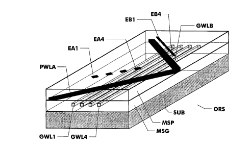
Figure 8 is a perspective view of a 4x4 switch. A glass -
cladding layer MSG, in which four glass waveguide cores
form glass waveguides GWL1...GWL4, is arranged on a
substrate SUB serving as carrier. Above the glass cladding
layer GMS is arranged a polymer cladding layer MSP in which
a polymer waveguide PWLA is embedded. The polymer
waveguide PWLA is shaped such that each glass waveguide
GWL1...GWL4 is intersected once at the angle a and once at
the complementary angle thereto. The intersection angles
have been greatly exaggerated in Figure 8 however. The
overlapping of the v~aveguides in the vertical direction
gives rise to 2x4=8 coupling regions. These can be
switched independently of one another with the aid of
heating elements EA1...EA4 and EB1...EB4 arranged on the
polymer cladding layer MSP. As can easily be deduced from
CA 02285711 1999-10-08
16
Figure 7, by means of this switch, light can be
bidirectionally switched over from every glass waveguide
GWL1...GWL4 into any other glass waveguide GWL1...GWL4.
When light of a different but closely adjacent wavelength
is guided in the glass waveguides GWL1...GWL4 (wavelength
multiplexing) this light can also be jointly guided in the
polymer waveguide PWLA without serious disturbances
occurring. In this arrangement all the optical waveguides
are straight so that no losses occur due to waveguide
curvatures.
Figure 9 illustrates a possibility whereby the glass
waveguides GWL1...GWL4 can be connected to optical fibres.
Apart from the actual switching region, the glass
waveguides GWL1...GWL4 are weakly curved in order thus to
allow a larger spacing between the connection points. The
connection points have the form of V-grooves VNUT into
which optical fibres are insertable. In contrast to the
exemplary embodiment shown in Figure 8, the bent polymer
waveguide PWLA shown therein has been replaced here by two
individual, straight polymer waveguides PWLA and PWLB.
In the exemplary embodiment illustrated in Figure 10 - not
to scale - the polymer waveguide PWLA is not straight
throughout, but only in the coupling regions. In between,
the polymer waveguide PWLA is curved in an s-formation.
The space requirement of the optical switch can be reduced
in this way. However this space saving is generally
acquired at the expense of light losses caused by the
curvatures. The heating electrodes have not been
illustrated here for reasons of clarity. In the production
of a switch according to the invention it is entirely
possible to resort to the use of known methods of producing
glass- and polymer waveguides. In this connection
reference will again be made to the above mentioned
publication by N. Keil in which further bibliographical
17
references are given.