Note: Descriptions are shown in the official language in which they were submitted.
CA 02285788 1999-10-08
1
Title of the Invention:
Method cf fabricating film for solar cells
AACKGROUND OF THE INVENTION:
Field of the Invention:
The present invention relates to a method of
fabricating Cu~x ( In;;Ga:-x; ~i (SeySi-y) Y film for solar cells.
Description of the Prior Art:
Solar cells in recent years have achieved a high
maximum conversion efficiency of 17.7 by using films
consisting of Cuoc (In:~Gal-x) ~i (SeySl-y) Y (hereinafter also
referred to as "CIGS"). However, when such films are grown
under conditions in which there is an excessive supply of
group III elements In and Ga, it is possible to fabricate
single phase CIGS, but it has a high defect density and
high resistance ~~hat degrade the properties of the
resultant solar cell. On the other hand, while using an
excess supply of Cu, a group I element, does provide large,
good-quality crystals, it also results in the surface and
boundary formation of the low resistance Cu-Se metal phase
that makes devices prone to short circuit.
In order to grow high-quality CIGS films for
solar cells, a complicated method is currently used,
comprising first using an excess supply of Cu to form
large-grain, high-quality CIGS, and followed by a step of
using excess Ga and In to thereby remove a Cu-Se phase on
the surface. Moreover, since a high temperature of around
550°C is used to ensure the adequate reaction of each
element, the method can only be used with substrates able
to withstand such temperatures.
An object of the present invention is to provide
a method of fabricating CIGS film for solar cells in which
the generation of point defects (divacancies) and twin-
CA 02285788 1999-10-08
2
crystal stacking faults is suppressed to thereby fabricate
high-quality film.
Another object of the invention is to simplify
the formation process by providing a method of fabricating
high-quality CIGS films ror solar cells in which the film
is formed at a low temperature.
SUMMARY OF THE INVENTION
In accordance with the present invention, the
obj ect is attained by a method of fabricating Cua (In;;Gal-
:~) (3 (SeySl-y) Y films for solar cells, said method comprising
forming an electrode on a substrate and supplying Cu, In,
Ga, Se, and S to the substrate via the electrode to form a
Cua(InXGal-x) ~ (SeyS~-,,)-y film and at the same time supplying
thereto water vapor or a gas containing a hydroxyl group,
wherein 0 s x _< 1, 0 < y s 1, and a, a, and Y are arbitrary
integers.
The objective is also attained by a method of
fabricating Cua (In,~Ga~-x) (3 (SeyS~-,,) Y film for solar cells, said
method comprising forming a Cua (In,;Gai-x) p (SeySi-y) Y film onto
a substrate in a vacuum chamber by depositing or sputtering
Cu, In, Ga, Se, and S on the substrate and at the same time
supplying to the substrate water vapor or a gas containing
a hydroxyl group, wherein 0 s x s 1, 0 s y s l, and a, (3,
and Y are arbitrary integers.
The objective is also attained by a method of
fabricating Cua(InxGal-X)~i(Se,rSl-y)Y film for solar cells, said
method comprising forming a Cua (InxGa~-x) a (Se,,Sl-y) Y film on
a substrate in a gas reaction chamber by effecting a flow
of gas to the substrate, that includes Cu, In, Ga, Se, and
S and at the same time supplying to the substrate water
vapor or a gas containing a hydroxyl group, wherein 0 s x
s 1, 0 s y s 1, and a, ~, and y are arbitrary integers.
CA 02285788 1999-10-08
3
The objective is also attained by a method of
fabricating Cua ( InxGa~-x) (3 (SeYS,-,.) Y film for solar cells, said
method comprising forming a Cua (In;;Gal-:~) (3 (SeySi-y) Y film on
a substrate in a vacuum chamber by depositing or sputtering
Cu, In, Ga, Se, and S on the substrate, then placing the
substrate in a gas reaction chamber and carrying out
annealing in a gaseous atmosphere containing Se, and
wherein during either or both of the deposition or
sputtering and the annealing the substrate is supplied with
water vapor or a gas containing a hydroxyl group, wherein
0 s x s 1, 0 s y s 1, and a, (3, and Y are arbitrary
integers.
As described in the foregoing, by supplying
water vapor or a gas containing a hydroxyl group during the
formation of the CIGS film, anion vacancies and cation-
anion composite vacancies that develop during the formation
of the film are suppressed by the anion vacancies being
filled with oxygen. As this also reduces the density of
twin crystals, which are correlated to anion vacancies, it
makes it possible to produce high-quality films for solar
cells.
Moreover, supplying at least one gas selected
from the group consisting of water vapor or a gas
containing a hydroxyl group during the formation of the
CIGS film enables the amount of Cu, In, Ga, Se, and S
supplied to be kept constant and the reaction temperature
to be reduced to around 450°C, thus simplifying the process
and expanding the range of substrates that can be used.
Further features of the invention, its nature and
various advantages will be more apparent from the
accompanying drawings and following detailed description of
the invention.
CA 02285788 1999-10-08
4
BRIEF EXPLANATION OF THE DRAWINGS
Figure 1 is a cross-sectional view of an example
of a solar cell using CIGS film fabricated by the method of
the present invention.
Figure 2 illustrates a first embodiment of the
method of the invention applied to the vacuum deposition
method.
Figure 3 is an explanatory view showing a
modification of the method of Figure 2, in which a
different method of supplying a gas is adopted.
Figure 4 illustrates a second embodiment of the
method of the invention applied to the chemical vapor-phase
epitaxial growth method.
Figure 5 illustrates a modification of Figure 4,
in which a different method of supplying a gas is adopted.
DESCRIPTION OF THE PREFERRED EMBODIMENTS
Figure 1 shows a cross-sectional view of ari
example of a CIGS solar cell 1 produced using the
fabrication method of this invention. Solar cell 1
comprises a glass substrate 2 on which are formed a
reverse-face electrode 3 of Mo or a similar substance, a p-
type Cua(InxGai-:~) (3 (SeYS~-,,)Y film 4, a buffer layer 5 and an
n-type Zn0 (or In20s) layer 6. Here, O S X S 1, 0 s y <_ 1,
and a, ~3, and y are arbitrary integers.
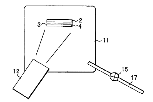
Figure 2 shows a first embodiment of the
fabrication method of the invention, applied to the vacuum
deposition method. rn Figure 2, the glass substrate 2 on
which has been formed i.he reverse-face electrode 3 is
placed in a vacuum chamber 11 and Cu, In, Ga, Se, and S
from a source 12 are sequentially deposited or sputtered
onto the reverse-face electrode 3 to form a CIGS film 4.
At the same time as the CIGS film 4 is being formed by the
CA 02285788 1999-10-08
5
deposition or sputtering, water vapor or a gas containing
a hydroxyl group is supplied from a source to the reverse-
face electrode 3.
Examples of substances generating hydroxyl group-
containing gases include a hydrogen peroxide solution
(H20z) , alcohols (C:zNsOt~ etc. ) , acids and alkali .
Thus, in the present invention, simultaneously
with~deposition or sputtering of Cu, In, Ga, Se and S,
water vapor or a gas containing a hydroxyl group is
supplied onto the reverse-face electrode 3 on the glass
substrate 2, thereby fabricating a CIGS film 4.
One example of supplying the water vapor or gas
containing a hydroxyl group to the vacuum chamber 11
is illustrated in rigure 2, in which a given gas is
directly supplied into the vacuum chamber 11 from a pipe 17
with the amount of the gas controlled by a variable valve
or mass flow controller 15.
Another example is illustrated in Figure 3 in
which oxygen gas taken via a pipe 16 is bubbled through
high purity water in a vessel 13 that has been heated to a
predetermined temperature set by means of a temperature
controller 14. This generates in the vessel 13 oxygen gas
and water vapor having a predetermined partial pressure.
This oxygen gas and water vapor are supplied to the vacuum
chamber 11 via the pipe 17. By thus supplying water vapor
or gas containing a hydroxyl group during the formation of
the CIGS film, anion vacancies and cation-anion divacanCies
that develop during the formation of the film are
suppressed by the anion vacancies being filled with oxygen.
This also reduces the density of twin crystals, which are
correlated to anion vacancies, and point defects and
stacking faults are also reduced, thereby making it
possible to obtain high-quality film for solar cells.
Figure 4 illustrates a second embodiment of the
CA 02285788 1999-10-08
6
fabrication method of this invention, applied to chemical
vapor-phase epitaxy. In Figure 4, the glass substrate 2 on
which has been formed the reverse-face electrode 3 is
placed in a gas reaction chamber 18, and Cu, In, Ga, Se and
S containing gases are run into the gas reaction chamber 18
via a conduit. 20. A carrier gas is simultaneously run into
the gas reaction chamber 18 via a conduit 19 so that the
raw-material gases are brought into contact with the
reverse-face electrode 3 on the substrate 2 to thus grow a
CIGS film 4 by vapor-phase epitaxy. In addition, water
vapor or a gas containing a hydroxyl group is
simultaneously supplied into the reaction chamber 18 via a
conduit 21 to provide the reverse-face electrode 3 on the
glass substrate 2 with water or the hydroxyl group. As a
result, the generation of point defects and twin-crystal
stacking faults in the CIGS film 4 is suppressed. Denoted
by reference numeral 22 is an outlet pipe for allowing the
gases to exit; .
Figure 5 illustrates a modification of the method
Figure 4, in which oxygen gas taken via a pipe 23 is
bubbled through high purity water in a vessel 24 that has
been heated to a predetermined temperature set by means of
a temperature controller 25. This generates in the vessel
24 oxygen gas and water vapor having a predetermined
pressure. This oxygen gas and water vapor are
simultaneously supplied to the reaction chamber 18 via the
pipe 26. Gases containing Cu, In, Ga, Se and S are
simultaneously introduced into the gas reaction chamber 18
via the pipe 20, thereby suppressing the formation of point
defects and twin-crystal stacking faults in the CIGS film.
The invention can also be applied to the
selenization method. Specifically, as in the first
embodiment or its modification, in the vacuum chamber 11
shown in,Figure 2 or Figure 3 Ca, In, Ga, Se and S are each
CA 02285788 1999-10-08
7
deposited or sputtered onto the reverse-face electrode 3 on
the glass substrate 2 to form a precursor film of Cua(In~Ga1-
x) (3 (SeYS~-Y)y. The substrate is then placed in the gas
reaction chamber 18 shown in Figure 4 or Figure 5 and, as
in Lhe second embodiment or its modification, a flow of Cu,
In, Ga, 5e, and S vapor is implemented to effect annealing
with HZSe or Se. In this selenization method, water vapor
or gas containing a hydroxyl group is supplied to the
vacuum chamber 11 as in the first embodiment, or to the gas
reaction chamber 18 as in the second embodiment, or to both
the vacuum chamber 7.1 and the gas reaction chamber 18.
A working example of fabricating a CIGS film for
a solar cell according to the present invention applied to
the vapor deposition method will be described.
A GaAs single crystal substrate was disposed in
a vacuum chamber. While the substrate temperature was kept
at around 450°C and Cu, In, Ga (Cu/(In+Ga): about U.8] and
excess Se were supplied into the vacuum chamber for about
60 minutes. During the supply of the raw materials, water
vapor and oxygen gas were supplied into the vacuum chamber
at 0.1 cc/min and l0 cc/min, respectively. As a result, a
CIGS film having a thickness of about 0.8 um was formed on
the substrate. By the addition of water vapor and oxygen
gas, the twin crystal density that was about 10.4% was
reduced greatly to 1.8a.
Based on the confirmed results of experiments
carried out to date by Lhe inventors, oversupplying group
zII elements In and Ga during the formation of the CIGS
film increases the volumetric ratio of twin crystals.
However, when, in accordance with the present invention,
water or a hydroxyl group is supplied at the same time as
the GIGS film is being fabricated, the twin crystal density
is greatly reduced as described above. Moreover, in the
CA 02285788 1999-10-08
8
case of conventional methods of forming films, a reaction
temperature of around 550°C was used to remove a phase
formed by an oversupply of a specific material. However,
since in the case of the method according to the present
invention the amount of each material supplied is constant
and an excess supply technique is not used, good-quality
films could be obtained with a reaction temperature of
around 450°C.
As described in the foregoing, supplying water
vapor or a gas containing a hydroxyl group during the
formation of the CIGS film makes it possible to suppress
the production of point defects (composite vacancies),
twin-crystal stacking fa~~)ts and other such defects, making
it possible to obtain high-quality CIGS film crystal, use
a lower temperature to grow the film and simplify the
formation process.