Note: Descriptions are shown in the official language in which they were submitted.
CA 02285871 1999-10-15
AMPLIFIER WITH FEEDFORWARD LOOPS
FOR REJECTING NON-LIrIEAR DISTORTION
BACKGROUND OF THE; INVENTION
1. Field of the Invention
The present invention relates to an amplifier with
feedforward (abbreviated hereinafter as FF) loops for rejecting
non-linear distortion and control circuitry for optimizing FF loops
which employs a method for compensating distortion generated in
a main amplifier. The present invention particularly relates to
a technique .for compensating distortion such as intermodulation
distortion generated in a main amplifier.
2. Description of Related Art
A base station or a relay stat_Lon for mobile communications
performs wireless transmission of a multicarrier signal including
a number of modulated carriers. More specifically, a base station
or a relay station modulates each of the multiple carriers and
arranges those carriers on a frequency axis at a certain frequency
separation to obtain a multicarrier signal. The base station or
the relay station then executes radio-frequency amplification (RF
amplification) of the obtained multi.carrier signal, and performs
wireless transmission of the multi~carrier signal after the RF
amplification. Accordingly, such a ;station requires an amplifier
for executing RF amplification of a multicarrier signal. Further,
in order to favorably communicate with a mobile station located
within a coverage or a cell, the station typically requires a RF
amplifier that can perform high power amplification. A similar
1
CA 02285871 1999-10-15
need also exists in a booster or like devices.
In an amplifier used for amplifying a multicarrier signal,
superior linearity is required over the entire frequency range to
which the multicarrier signal belongs because, if the linearity
of the amplifier is not sufficient, normal and high-quality
communication would be obstructed b:y distortion generated in the
amplifier. A variety of distortions exist that are caused by the
non-linearity of the amplifier. Among those distortions,
distortion being produced at a frequE~ncy identical to or extremely
close to that of a carrier like IMD ( intermodulation distortion )
cannot be, or remains very difficult to be, eliminated by an
approach such as providing a t=Llter after the amplifier.
Nevertheless, distortions having such nature are likely to occur
when amplifying a multicarrier signal.
One approach for providing an ,~mplif ier having an extremely
low amount of distortion which i~~ suitable for amplifying a
multicarrier signal is to improve the linearity of the amplifier
by adding circuitry to the amplifier. One known example technique
of such an approach is the FF amplification method disclosed in
Japanese Patent Laid-Open Publication No. Hei 4-70203. An
amplifier adopting the FF amplification method comprises a
distortion detection loop and a di~~tortion rejection loop.
The signal path from the signal_ input terminal to the signal
output terminal passing through the main amplifier, that is, the
signal path for transmitting the input signal into the main
amplifier to be amplified and the signal amplified by the main
amplifier, is referred to as the dominant path. To simplify
notation in the present application, the signal transmitted in the
dominant path is hereinafter referrE~d to as the dominant signal.
2
CA 02285871 1999-10-15
The signal passing through the dominant path before the main
amplifier is referred to as the input signal. The signal passing
through the dominant path from the output terminal of the main
amplifier to the point of being subjected to distortion
compensation is referred to as thE~ output signal. The signal
passing through the dominant path after the point of distortion
compensation is referred to as the distortion-compensated output
signal.
The distortion detection loo~> provides as a feedforward a
first branch signal obtained by branching a portion of the input
signal at a first branching point to <~ first coupling point located
thereafter. At a second branching point located after the first
branching point and a main amplifier, a portion of the output signal
is branched as a second branch signal. The second branch signal
and the first branch signal provided as a feedforward are combined
at the first coupling point.
The input signal and the f_Lrst branch signal branched
therefrom include a plurality of carrier components constituting
the multicarrier signal, but do not, at any time, include distortion
components generated in the main amplifier or its surrounding
circuitry (hereinafter collectively referred to as "the main
amplifier"). On the other hand, when distortion components are
being generated in the main amplifiE~r, the output signal and the
second branch signal branched therefrom include both the carrier
components and the distortion components. Accordingly, when
combining the first and the second branch signals, if the first
and the second branch signals to be combined are in a relationship
such that their respective carrier ~~omponents cancel each other
out, a signal including only the distortion components can be
3
CA 02285871 1999-10-15
obtained. A signal obtained as suc;h is hereinafter referred to
as the distortion signal.
To obtain a highly pure distortion signal having only the
distortion components, the first and the second branch signals must
be in a relationship such that their respective carrier components
completely cancel each other. Specifically, a first requirement
for this relationship is that the Electrical wave length of the
signal path from the first branching point to the first coupling
point passing through the distortion detection loop must be
identical with the electrical wave 7_ength of the signal path from
the first branching point to the j=first coupling point passing
through the main amplifier and thE~ second branching point . A
second requirement is that, at the first coupling point, the first
and the second branch signals must have an identical amplitude and
an opposite phase from one another.,
The distortion rejection loop provides the distortion signal
as a feedforward to be recombined with the output signal at a second
coupling point located after the first and the second branching
points. If the signal delay occurring in the distortion rejection
loop is compensated in the dominant path, and if the distortion
components in the output signal and i~he distortion signal through
the auxiliary amplifier are appropriately adjusted in the
distortion rejection loop or in the dominant path such that their
respective amplitudes are identical and their phases are opposite
from one another, the signal recombining operation at the second
coupling point rejects distortion components generated in the main
amplifier to provide a distortion-compensated output signal having
no, or a suppressed amount of, distortion components.
Fig. 8 shows an example configuration of a conventional FF
4
CA 02285871 1999-10-15
amplifier. In this amplifier, thrE~e hybrids HYB1-HYB3 are used
to form the distortion detection loop Ll and the distortion
rejection loop L2. In the Figure, the signal path from the signal
input terminal IN to the signal output terminal OUT passing through
the main amplifier A1 and the coaxia_L delay line D2 is the dominant
path. The signal path from the first branching point inside hybrid
HYB1 to the first coupling point inside hybrid HYB2 passing through
the coaxial delay line D1 is the distortion detection loop L1. The
signal path from the first coupling point to the second coupling
point inside hybrid HYB3 passing through the auxiliary amplifier
(distortion amplifier) A2 is the distortion rejection loop L2.
Respective dummy loads ZO in the Figure have an impedance equal
to the characteristic impedance of ithe transmission line, and is
used as the termination for hybrids HYB1 and HYB3 terminals. The
second branching point is located _Lnside hybrid HYB2.
The signal applied to the signal input terminal IN, namely,
the input signal, is a multicarrie:r signal, for example. This
signal is input, via hybrid HYB1, into variable attenuator ATT1
and variable phase shifter PS1. After being subjected to amplitude
and phase adjustment therein, the input signal is amplified by the
main amplifier A1. The signal amplii'ied by the main amplifier A1,
namely, the output signal, is input into hybrid HYB3 via hybrid
HYB2 and the coaxial delay line Dc'.. Further, the distortion-
compensated output signal is output from hybrid HYB3 to subsequent
circuitry via the signal output terminal OUT. The coaxial delay
line D2 is the delay line for compensating the delay exerted on
the distortion signal by the circuitry that constitute the
distortion rejection loop L2 including the auxiliary amplifier A2.
Furthermore, the input signal is branched into two signals
5
CA 02285871 1999-10-15
by hybrid HYB1. The two branched :signals are identical signals
with respect to frequency structure of their components. One of
the two branched signals which is to be provided in the dominant
path is supplied to the main amplifier A1 as the input signal and
is thereby amplified. The other of i~he two branched signals which
is to be provided in the distortion detection loop L1, namely, the
first branch signal, is supplied from hybrid HYB1 to hybrid HYB2
via the coaxial delay line D1 while its amplitude is mostly
maintained as is. The coaxial delay line D1 is the delay line for
compensating the delay exerted on the dominant signal by the
circuitry of the dominant path, especially the main amplifier A1.
At the second branching point located therein, hybrid HYB2
branches into two signals the signal output from the main amplifier
A1 including distortion components. The two branched signals are
identical signals with respect to frequency structure of the
components. One of the two branched signals is supplied to the
dominant path as the output signal. The other of the two branched
signals, namely, the second branch signal, is combined with the
first branch signal in the first coup:Ling point inside hybrid HYB2.
If the distortion detection loop L1 is optimized as described below,
this combining operation in hybrid HYB2 cancels the carrier
components in the first and the second branch signals, producing
the distortion signal indicating the distortion components
generated in the main amplifier A1.
The distortion signal obtained in this way is supplied from
hybrid HYB2 sequentially to variab7Le attenuator ATT2, variable
phase shifter PS2, and the auxiliary amplifier A2, constituting
the distortion rejection loop L2. ;3pecifically, the distortion
signal is subjected to amplitude and phase adjustment in variable
6
CA 02285871 1999-10-15
attenuator ATT2 and variable phase shifter PS2, amplified by the
auxiliary amplifier A2, and input into hybrid HYB3. The distortion
signal input into hybrid HYB3 is combined in the second coupling
point inside hybrid HYB3 with the dominant signal transmitted via
the coaxial delay line D2. If both of the distortion detection
loop L1 and the distortion rejection loop L2 are optimized as
described below, this combining operation in hybrid HYB3 produces
the distortion-compensated output signal in which the distortion
components are eliminated or suppressed (by canceling out). The
distortion-compensated output sign~~l is output from the signal
output terminal OUT.
To generate a highly pure distortion signal by combining the
first and the second branch signals and canceling out the carrier
components, a predetermined number oi:carrier componentscontained
in respective ones of the first and the second branch signals must
have an identical timing, an identical amplitude, and an opposite
phase from one another at the first. coupling point. To fulfill
these requirements, that is, to optimize the distortion detection
loop L1, the circuit shown in Fig. 8 is provided with the coaxial
delay line D1 as means for providing an identical timing to the
respective carrier components, and variable attenuator ATT1,
variable phase shifter PS1, and the control circuit 10 as means
for providing an identical amplitude and an opposite phase to the
respective carrier components. The control circuit 10 is the means
for adjusting the output of hybrid HYB2 such that a distortion
signal including primarily only the distortion components and no
carrier components is supplied to the auxiliary amplifier A2 . This
adjustment is performed in the control circuit 10 by adjusting and
controlling the signal attenuation c,l and the phase shift 81 in
7
CA 02285871 1999-10-15
variable attenuator ATT1 and variat>le phase shifter PS1 to their
respective optimal values.
To generate a favorable distortion-compensated output signal
through combining the output signal and the distortion signal, it
is preferred that the distortion signal transmitted via the
auxiliary amplifier A2 primarily includes no carrier components
but only the distortion components. This can be fulfilled by
optimizing the distortion detection loop L1, because, as long as
the distortion detection loop Ll is operating normally, distortion
generating in the auxiliary amplifier A2 can be ignored. The
second requirement in compensating distortion generated in the main
amplifier A1 is that, at the second coupling point, the distortion
components in the output signal transmitted via the coaxial delay
line D2 and those in the distortion signal via the auxiliary
amplifier A2 must have an identical t~Lming, an identical amplitude,
and an opposite phase with respect to one another. To fulfill this
second requirement, that is, to optimize the distortion rejection
loop L2, the circuit shown in Fig. 8 is provided with the coaxial
delay line D2 as means for providing an identical timing to the
distortion components in respective signals, and variable
attenuator ATT2, variable phase shifter PS2, and the control
circuit 10 as means for providing an identical amplitude and an
opposite phase to the distortion components in respective signals.
The control circuit 10 adjusts and controls the signal attenuation
G2 and the phase shift 8 2 in variable attenuator ATT2 and variable
phase shifter PS2 to their respective optimal values to generate
a distortion-compensated output signal in which the distortion
components are eliminated or suppressed.
The control circuit 10 executes the adjustment and control
8
CA 02285871 1999-10-15
of the above-mentioned G1, 8 1, G2, and 8 2 to their optimal values,
which are the processes for optimi:aing the distortion detection
loop L1 and the distortion rejecti~~n loop L2. In Fig. 8, these
optimizing processes are executed by the control circuit 10 through
insertion and detection of two kinds of pilot signals under the
control of the CPU.
The control circuit 10 comprises oscillators OSC1 and OSC2,
and is connected with directional couplers DC1-DC4. Oscillators
OSC1 and OSC2 generate the pilot signals for L1 and L2,
respectively.
Directional coupler DC1 conr.~ected to oscillator OSC1 is
disposed before the first branching point located inside hybrid
HYB1, so as to insert the pilot signal for L1 into the input signal
and the first branch signal branched therefrom. Directional
coupler DC2 is disposed along the path between the first coupling
point inside hybrid HYB2 and the second coupling point inside hybrid
HYB3 passing through the auxiliary amplifier A2, so as to detect
the presence of the pilot signal :Eor L1 and its level in the
distortion signal.
Directional coupler DC3 connected to oscillator OSC2 is
disposed along the path between the first branching point inside
hybrid HYB1 and the second branching point inside hybrid HYB2
passing through the main amplifier A1 (may be inside the main
amplifier A1), so as to insert the pilot signal for L2 into the
output signal and the second branch signal branched therefrom.
Directional coupler DC4 is disposed between the second coupling
point inside hybrid HYB3 and the signal output terminal OUT, so
as to detect the presence of the pilot signal for L2 and its level
in the distortion-compensated output signal.
9
CA 02285871 1999-10-15
The control circuit 10 inserts or superimposes the pilot
signal for L1 in the input signal using directional coupler DC1,
and detects the pilot signal for L1 using directional coupler DC2.
The control circuit 10 controls the signal attenuation G1 and the
phase shift 81 such that the detect=ed level of the pilot signal
for L1 becomes lower in directional coupler DC2, thereby optimizing
the distortion detection loop L1. In other words, the signal
attenuation G1 and the phase shift 81 are controlled such that
the pilot signal for L1 does not appear in the distortion signal.
Further, the control circuit 10 inserts or superimposes the
pilot signal for L2 in the output signal using directional coupler
DC3 before the second branching point., and detects the pilot signal
for L2 using directional coupler DC4. The control circuit 10 then
controls the signal attenuation G2 and the phase shift 82 such
that the detected level of the pilot= signal for L2 becomes lower
in directional coupler DC4, thereby optimizing the distortion
rejection loop L2. In other words, 'the signal attenuation G2 and
the phase shift 8 2 are controlled such that the pilot signal for
L2 does not appear in the distortion-compensated output signal.
Processes for determining G1, 8 1, G2, and B 2 are primarily
executed by the CPU 12 and the control signal generator 14 inside
the control circuit 10.
Out-of-band undesired signals are first eliminated from the
signals detected in directional couplers DC2 and DC4 using
band-pass filters BPF1 and BPF2, respectively. To further
facilitate signal handling, these s~Lgnals are then mixed with an
oscillated output of the local oscillator LOC using mixers MIX1
and MIX2. From among the resulting signals, low-pass filters LPF1
and LPF2 extract the difference frequency components, namely, the
CA 02285871 1999-10-15
signals converted to a lower frE~quency than original. The
extracted components are input into the control signal generator
14 via amplifiers or buffers B1 and B2. The control signal
generator 14 generates control sign<~ls related to G1, 81, G2, and
B 2 under the control of the CPU 12 following a step-by-step logic
and method. The step-by-step method herein refers to a repeated
sequential execution of the process of slightly shifting the values
of the control signals in an arbitrary direction to search for the
direction of change toward which the output levels from amplifiers
or buffers B1 and B2 would be lower, and changing the control signal
values in that direction.
Although an amplifier Having an extremely low amount of
distortion suitable for amplification of a multicarrier signal can
be formed according to the above-described circuit arrangement,
several problems still remain.
When there are changes in, for Example, the level of the input
signal, the number of carriers, and temperature level, operating
conditions are altered in the main amplifier A1 and the auxiliary
amplifier A2. If the control signals are generated by the
step-by-step process as described above, it is difficult to follow
rapidly such an alteration in operating conditions of the main
amplifier A1 and the auxiliary amplifier A2 upon its occurrence.
In other words, the time it takes for the loops to balance under
the new operating conditions after allterations and for the detected
levels of the pilot signals to accordingly settle close to zero,
namely, the acquisition time of the loops with respect to
alterations in operating condition;, becomes long such that it
cannot in practice be ignored.
Especially, if the above-described conventional technique
11
CA 02285871 1999-10-15
is used in the above-mentioned :Field of RF amplifiers for
transmission in a base station for mobile communications, for
example, the acquisition time of the loops with respect to
alterations in operating conditions miay be as long as 3 to 10 seconds.
Moreover, the auxiliary amplifier A;2 may receive excessive input
during the time period from the occurrence of an operating condition
alteration to the balancing of the distortion detection loop L1,
and, when such state is notable, the auxiliary amplifier A2 may
become damaged.
As the pilot signal for L1 is .included in the output signal
transmitted via the coaxial delay line D2, the pilot signal for
L1 undesirably remains in the distortion-compensated oui~put signal .
The residual pilot signal for L1 may become an impediment to
operation in subsequent circuitry. For example, in the
application of RF amplifier for transmission in a base station for
mobile communications, undesirable ~~purious effect is caused when
the distortion-compensated output signal having residual pilot
signal for L1 is supplied as is to an antenna.
To prevent such undesirable effects by using additional
circuitry in the circuit of Fig. 8, for example, a notch filter
for blocking the pilot signal for L1 may be disposed in a section
after the second branching point inside hybrid HYB2 along the
dominant path. Alternatively, a circuit may be provided for
injecting into the dominant path a signal that cancels out the pilot
signal for L1. However, as the notch :Filter would filter the signal
amplified by the main amplifier A1 h~~ving high power, a large and
expensive notch filter must be used. In addition, disposing a
notch filter would cause degradation in phase linearity of the
entire circuit. Generation of insertion loss by the notch filter
12
CA 02285871 1999-10-15
would also lower the operating efficiency of the entire circuit.
A circuit for injecting into the dominant path a signal that cancels
out the pilot signal for L1, on the other hand, is not practical
because its structure would be complex and the control for
temperature compensation or the like would be difficult.
SUMMARY OF THE INVENTION
One object of the present invention is to eliminate the
necessity for the pilot signal for L1. By doing away with the pilot
signal for L1, undesirable spurious effects can be prevented
without using a notch filter or a circuit for canceling the pilot
signal for L1. Accordingly, a FF annplifier can be provided that
generates less spurious radiation, has a smaller size, and is less
costly compared to the conventional types. In the present
invention, this object is achieved by newly adopting a
synchronizing detectorfor the control of the distortion detection
loop.
Another object of the present invention is to eliminate the
step-by-step process performed by the CPU and thereby provide a
highly reliable FF amplifier with its loops having more reduced
acquisition time. In the present invention, this object is
accomplished by providing a synchron_Lzing detector for the control
of the distortion detection loop and the distortion rejection loop.
When an input signal comprising a plurality of carriers, each
having a different frequency from one another, is amplified and
output by a main amplifier, the present invention compensates the
distortion components included in the output signal from the main
amplifier.
13
CA 02285871 1999-10-15
The present invention may be innplemented as follows . First,
a distortion signal is generated by combining, at the first coupling
point, the first branch signal branched from the input signal at
the first branching point with the aecond branch signal branched
from the output signal at the second lbranching point. As the first
branch signal is a signal branched from the input signal, the first
branch signal includes a plurality oj: carriers but does not include
any distortion generated in the main amplifier. The second branch
signal is a signal branched from the output signal which is obtained
by amplifying the input signal in the main amplifier. The second
branch signal therefore includes not only the above mentioned
plurality of carriers but also the distortion generated in the main
amplifier. In the present invention, amplitude and phase
adjustments are conducted in any one of the plurality of signal
paths between the first branching point and the first coupling point
according to a control signal, in order to prevent the carrier
components included in the first and i~he second branch signals from
leaking into the distortion signal when combining those branch
signals. As a result, the carrier components cancel out one
another, and a distortion signal can be obtained wherein primarily
only the distortion components remain. By using the distortion
signal obtained in this way, the distortion components included
in the output signal from the main amplifier can be compensated,
thereby producing a distortion-compensated output signal.
One feature of the present invention is that the distortion
signal is subjected to synchronizing detection using a regulated
reference signal containing the above mentioned plurality of
carrier components. This reference signal is produced by
branching a third branch signal from any one of the input signal,
14
CA 02285871 1999-10-15
output signal, or distortion-compensated output signal, and by
regulating the level of the third branch signal such that the
average power of the reference sign;~l does not vary even when the
total average power of the respect_Lve carriers constituting the
signal varies. The third branch signal may also be branched from
the first or the second branch signal. In the present invention,
the signal obtained as a result of the synchronizing detection is
used as the control signal for controlling the amplitude and phase
adjustment operations at the time of distortion signal generation.
In this way, in the present invention, the control signal
is generated through performing synchronizing detection of the
distortion signal. Accordingly, no pilot signal is necessary for
distortion detection, and generation of undesirable spurious
effects caused by such pilot signals can be prevented. It is
therefore no longer necessary to provide circuits or devices such
as notch filters for preventing radiation of such undesirable
spurious effects, allowing smaller size and lower cost. Further,
as the control signal is produced through the synchronizing
detection, the conventional step-by-step monitoring and control
process can be eliminated, thereby enabling high speed acquisition .
Moreover, operation of a synchronizing detector for the
synchronizing detection can be stable and reliable over a
relatively wide range of operating levels because the signal
produced as the reference signal for the synchronizing detection
is generated by regulating the signal level, for example, through
Automatic Level Control (ALC ) , of the input signal or a signal that
similarly contains the plurality of carrier components. The
stabilization of operation of the synchronizing detector also
applies to the synchronizing detector on the distortion rejection
CA 02285871 1999-10-15
loop side described later.
The FF amplifier embodying the present invention comprises
distortion detection means and distortion compensation means.
The distortion detection means may, for example, include a
main amplifier, a distortion detection loop, and first amplitude
and phase adjustment means. The distortion detection loop is a
circuit that generates the distortion signal by combining the first
branch signal and the second branch signal. The first amplitude
and phase adjustment means perform amplitude and phase adjustment
on a signal related to the main amplifier based on a first control
signal, such that only the distortion components contained in the
output signal from the main amplifier are extracted during the
signal combining process in the di~~tortion detection loop. The
first control signal is a signal for controlling the amplitude and
phase adjustment operations performed on the signal related to the
main amplifier at the time of the si~~nal combining process in the
distortion detection loop.
The distortion compensation means is the means for generating
a distortion-compensated output signal. The distortion
compensation means may, for example, comprise an auxiliary
amplifier, a distortion rejection loop, and second amplitude and
phase adjustment means. The distortion rejection loop generates
a distortion-compensated output signal by recombining the
distortion signal with the output si~~nal from the main amplifier.
The second amplitude and phase adjust=ment means perform amplitude
and phase adjustment on a signal related to the auxiliary amplifier
based on a second control signal,, such that the distortion
components do not leak from the out~~ut signal or the distortion
signal into the distortion-compensated output signal during the
16
CA 02285871 1999-10-15
signal recombining process in the distortion rejection loop. The
second control signal is a signal i=or controlling the amplitude
and phase adjustment operations pel°formed on the signal related
to the auxiliary amplifier at the time of the signal recombining
process in the distortion rejection loop.
For the generation of the fir~;t control signal, the control
circuit includes an ALC circuit and a first synchronizing detector.
The ALC circuit generates a reference signal by regulating the level
of the input signal or a signal similarly containing the plurality
of carrier components, such that the .average power of the reference
signal does not vary even when thE~ total average power of the
respective carriers constituting t:he signal varies. The first
synchronizing detector uses this reference signal to perform
synchronizing detection of the distortion signal. In the present
invention, the above-described first control signal is generated
in this way.
For the generation of the second control signal, the control
circuit includespilot signal insertion means, signal branch means,
and a second synchronizing detector. The pilot signal insertion
means inserts a pilot signal into I:he output signal before the
second branching point. The pilot signal is therefore present in
both the second branch signal and the distortion signal.
Accordingly, when the distortion rej ection loop is not optimized,
the pilot signal appears in the distortion-compensated output
signal. The signal branch means branches the distortion-
compensated output signal to produce a fourth branch signal. The
third branch signal and the fourth branch signal may be the same
signal. The second synchronizing detector performs synchronizing
detection of the fourth branch sign~~l using the pilot signal as
17
CA 02285871 1999-10-15
the reference. In this way, the residual amount of pilot signal
in the distortion-compensated output: signal can be determined, and
the second control signal can be generated accordingly.
As described above, the present invention can be expressed
as a distortion compensation method suitable for compensating
distortion in a FF amplifier, a control circuit that can be used
for a FF amplifier, and also as a FF amplifier. Furthermore, the
present invention may be practiced in a variety of embodiments.
Amplitude and phase adjustment in each of the loops may be
executed through vector modulation of the corresponding signals.
A vector modulator for this purpose may be implemented using a mixer
or like devices.
Concerning the distortion signal to be subjected to
synchronizing detection, it may be desirable to convert this signal
into a signal having lower frequE~ncy prior to synchronizing
detection.
The pilot signal for optimizing the distortion rejection loop
is preferably subjected to spectral spreading prior to its
insertion. In that case, the fourth branch signal is subjected
to spectral despreading prior to synchronizing detection. By
these procedures, interference between the pilot signal and the
carrier components is prevented.
The pilot signal may be more preferably oscillated at a low
frequency and converted to a frequency within the operating
frequency band of the main amplif_Ler prior to its insertion.
Further, prior to synchronizing detE~ction using the pilot signal
as the reference, the fourth branch signal is converted to the same
frequency as that of the pilot si~~nal. Oscillation at a low
frequency facilitates handling of signals.
18
CA 02285871 1999-10-15
Also preferably, with respect to the pilot signal, spectral
spreading may precede conversion to a frequency within the
operating frequency band of the main amplifier. The fourth branch
signal is converted to the same frequE~ncy as that of the pilot signal,
and is subsequently spectral despread.
BRIEF DESCRIPTION Ol? THE DRAWINGS
Fig. 1 is a diagram illustrating a circuit configuration
according to one embodiment of the present invention;
Fig. 2 is a diagram showing a configuration of a synchronizing
detector in the present embodiment;
Fig. 3 is a diagram showing a configuration of an ALC circuit
in the present embodiment;
Fig . 4 is a diagram showing a variation example of a component
for amplitude and phase adjustment in the present embodiment;
Fig . 5 is a diagram illustrating an example vector modulator;
Fig. 6 is a diagram showing a variation example of a control
circuit in the present embodiment;
Fig . 7 is a diagram showing a variation example of the control
circuit, especially of a section related to its distortion
rejection loop, in the present embodiment;
Fig. 8 is a diagram showing an example configuration of a
conventional FF amplifier; and
Fig. 9 is a diagram illustrating, as a reference example,
a variation configuration of the FF amplifier shown in Fig. 8 based
on the art of U.S. Patent No. 5528196.
19
CA 02285871 1999-10-15
DESCRIPTION OF THE PREI~ERRED EMBODIMENT
A preferred embodiment of the present invention will now be
described referring to accompan~~ing drawings. Similar or
corresponding components as those that appear in the conventional
circuit shown in Fig. 8 and the rei:erence circuit shown in Fig.
9 are labeled with identical reference numerals, to avoid
redundancy, explanations of those components will not be repeated.
(1) Embodiment
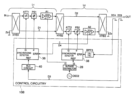
Fig. 1 illustrates a circuit configuration according to an
embodiment of the present invention. The circuit shown in this
Figure comprises a control circuit lOB including synchronizing
detectors 36, 38 and an ALC circuit 40.. The synchronizing detectors
36 and 38 are disposed correspondin<~ to the distortion detection
loop Ll and the distortion rejection loop L2, respectively. Each
of the synchronizing detectors 36 and 38 performs synchronizing
detection of the error signal denoted ERR in the Figure using the
signal denoted REF as a reference s~:gnal (i.e., the error signal
component in synchronism with respe~~t to the reference signal is
detected). Among the signals obtained by the synchronizing
detection, the gain control signal G is the signal for controlling
the corresponding variable attenuato~_°, and the phase control signal
8 is the signal for controlling the corresponding variable phase
shifter.
An example of the synchronizin~~ detectors 36 and 38 is shown
in Fig. 2. In this example, hybrid HYB5 converts the error signal
ERR into signals (ERRI, ERRQ) that are mutually orthogonal in the
phase space, and outputs those signals. An in-phase distributor
CA 02285871 1999-10-15
42 performs in-phase two-way division of the reference signal REF.
The example further comprises mixers MIX7 and MIX8 preferably in
the form of DBM (Double Balanced Mixers), differential amplifiers
IC1 and IC2 preferably in the form of: amplifiers having integrated
circuit structure, and offset adjustment circuits 44 and 46 for
adjusting the offset voltages of mixers MIX7 and MIX8.
Mixer MIX7 mixes the signal ERRI (0[rod]) from hybrid HYB5
and the reference signal REF from thE~ in-phase distributor 42, and
applies the obtained signal to the input terminal (non-inverted
input terminal in the Figure) of diffE~rential amplifier IC1. Mixer
MIX8 mixes the signal ERRQ ( -TL' /2 ( r<~d] ) from hybrid HYB5 and the
reference signal REF from the in-pha:~e distributor 42, and applies
the obtained signal to the input term_Lnal of differential amplifier
IC2. Differential amplifiers IC1 and IC2 amplify and output those
signals. Voltage occurring at the output terminal of differential
amplifier IC1 is used as the gain control signal G supplied to
variable attenuator ATTl or ATT2. Voltage occurring at the output
terminal of differential amplifier Ic~2 is used as the phase control
signal B supplied to variable phase shifter PS1 or PS2.
Connected to another input terminal ( inverted input terminal
in the Figure) on each of differential amplifiers IC1 and IC2 are
a capacitor C one end of which is connected to the output terminal,
a resistor R one end of which is grounded, and an of f set adjustment
circuit 44 or 46. Offset adjustment circuits 44 and 46 are circuits
for canceling offset voltages generated at the levels of some mV
in respective mixers MIX7 and MIX8. Offset adjustment circuits
44 and 46 generate necessary adjustment voltages for this purpose,
and apply the voltages as the reference voltages to differential
amplifiers IC1 and IC2. It is noted that the outputs from mixers
21
CA 02285871 1999-10-15
MIX7 and MIX8, after being subjected to differential amplification
in differential amplifiers IC1 and IC2, must possess a polarity
that applies negative feedback to the FF loop. Accordingly, to
which of the input terminals, invertE~d or non-inverted, the outputs
from mixers MIX7 and MIX8 is applied is determined depending on
the operation characteristics of each of the variable attenuators
and the variable phase shifters. It is then obvious to which of
the input terminals of differential amplifiers IC1 and IC2 the
reference voltages would be applie~~.
The control circuit lOB shown in Fig. 1 comprises the
above-described synchronizing detectors 36 and 38, the ALC circuit
40 for supplying a reference signal to synchronizing detector 36,
oscillator OSC2 for oscillating the pilot signal for L2, and the
in-phase distributor 28 for performing in-phase two-way division
of the pilot signal for L2. Further, the control circuit lOB is
connected with directional coupler Dc~2 located within the path from
the first coupling point in hybrid HYB2 to the second coupling point
in hybrid HYB3 passing through the auxiliary amplifier A2. The
control circuit lOB is also connected with directional coupler DC3
located within the path from the first branching point in hybrid
HYB1 to the second branching point in hybrid HYB2 passing through
the main amplifier A1 (DC3 may be disposed inside the main amplifier
A1 ) . The control circuit lOB is further connected with directional
couplers DC4 and DC9 located between the second coupling point in
hybrid HYB3 and the signal output terminal OUT . In addition, the
control circuit lOB comprises a band-pass filter BPF3 for
eliminating out-of-band noise from the output from directional
couplers DC4. Directional coupler DC9 may be disposed in any
location as long as it can detect ~~ signal having an identical
22
CA 02285871 1999-10-15
carrier arrangement as that of the input signal.
Synchronizing detector 36 receives the error signal ERR,
which is the distortion signal, from directional coupler DC2 via
coaxial delay line D4, and the reference signal REF, which is the
third branch signal, from directiona:L coupler DC9 via coaxial delay
line D3 and the ALC circuit 40. Coaxial delay lines D3 and D4
compensate the difference in electrical wave length between the
signal paths from the respective directional couplers to
synchronizing detector 36. The ALC circuit 40 automatically
controls the level of the signal transmitted through coaxial delay
line D3 to maintain the reference signal at a fixed level even when
the carrier average power varies. This prevents the change in DC
offset in mixers MIX7 and MIX8 inside synchronizing detector 36
(as described later).
Synchronizing detector 38 receives the error signal ERR,
which is the fourth branch signal, from directional coupler DC4
via the band-pass filter BPF3, ar,~d the reference signal REF
distributed by the in-phase distributor 28. The other remaining
signal of the divided output from the in-phase distributor 28 is
inserted into the signal in the dominant path as the pilot signal
for L2 using directional coupler D~'.3.
In the present arrangement, offset voltages in the
above-described mixers MIX7 and MIX8 are inherent to respective
mixers, and, in addition, vary depending on the local level of the
mixers. The inherent differences i.n offset voltages among the
individual mixers can generally be compensated by the above-
described offset adjustment circuit; 44 and 46. However, offset
adjustment circuits 44 and 46 cannot compensate for changes in
offset voltages due to alterations i.n the level of the reference
23
CA 02285871 1999-10-15
signal REF, namely, alterations in the local level. When an offset
voltage changes following an alteration in the local level, the
value of the control signal G or B deviates from the optimal value
for variable attenuator ATT1 or AT~~2 and variable phase shifter
PSl or PS2, resulting in loss of the balanced state of the distortion
detection loop L1 or the distortion rejection loop L2. In the
present embodiment, to maintain the local levels of mixers MIX7
and MIX8 at fixed levels, a signal i:rom oscillator OSC2, namely,
a signal having a stable level, is supplied to synchronizing
detector 38, and the output from the A~GC circuit 40, namely, a signal
subjected to level stabilizing processing, is supplied to
synchronizing detector 36, to serves as reference signals REF in
respective synchronizing detectors..
As shown in Fig . 3, the ALC circuit 40 comprises the following
components. Variable attenuator ATT3 adjusts the amplitude of the
signal from directional coupler DC9 disposed within the dominant
path. Hybrid junction HYB6 performs two-way division of the signal
subjected to this amplitude adjustment. Amplifier or buffer B3
is disposed between variable attenuator ATT3 and hybrid HYB6.
Further, in the ALC circuit 40, a detector DET detects one of the
branched outputs from hybrid HYB6 and outputs the resulting
detected voltage. The ALC circuit 40 further includes
differential amplifier IC3, which is preferably implemented using
an integrated circuit, for amplifying the detected voltage.
The signal from directional coupler DC9 is input into hybrid
HYB6 via variable attenuator ATT3 and amplifier or buffer B3. One
of the branched outputs from hybrid HYB6 is detected by the detector
DET having a structure that activates a detection diode in a
square-law detection area. The detE~cted voltage is supplied as
24
CA 02285871 1999-10-15
the attenuation ratio control signal via differential amplifier
IC3 to variable attenuator ATT3 located before hybrid HYB6.
Through attenuation ratio control by variable attenuator ATT3, the
other branched output from hybrid HYB6 is maintained at a fixed
output level within a sufficiently wide dynamic range.
The detector DET may be configured, for example, as disclosed
by the present applicant in Japanese Patent Application No. Hei
10-119292 and No. Hei 10-250582. In this configuration, a
temperature compensation diode is disposed in parallel with a
detection diode. These diodes are biased in the forward direction
under identical conditions, and temperature compensation is
performed according to the forward. voltage of the temperature
compensation diode. When the detecaion diode constituting the
detector DET is activated in a square-law detection area, the
detector DET operates in the average <~etection mode . Accordingly,
the level of the reference signal REF supplied from the ALC circuit
40 to the synchronizing detector 36 is prevented from being altered
only by changes in the number of carriers, presence or absence of
modulation, and variations in modu:Lation methods. In general,
when a detection diode is activated in a square-law detection area,
problems occur such as fluctuations in forward voltage due to
temperature change, generation of non-linear distortion due to such
forward voltage fluctuations, and non-uniformity in detection
efficiency. However, these problems are suppressed by using the
detector DET having the configuration of the above-mentioned patent
application.
(2) Advantages and Examples
According to the above-described embodiment, as the control
CA 02285871 1999-10-15
related to optimization of the dist:ortion detection loop L1 and
the distortion rejection loop L2 is ;performed using synchronizing
detectors 36 and 38, a CPU need not be provided to execute the
step-by-step procedure, allowing :.peed-up of loop response to
changes in operating conditions. For example, while the
acquisition time in a conventional example shown in Fig . 8 is 3-10
seconds, the acquisition time in the present embodiment is reduced
approximately to several hundred microseconds in the distortion
detection loop and several ten mi7_liseconds in the distortion
rejection loop. As a result, excessive input into the auxiliary
amplifier A2 is less likely to occur.
In the present embodiment, the pilot signal for L1 can be
eliminated because the synchronizing detector 36 is provided for
directly performing synchronization processing on the dominant
signal, and the distortion detection loop L1 is controlled in
accordance with the output from they synchronizing detector 36.
This results in the advantages oi= simplification in circuit
configuration and cost reduction, as. it is no longer necessary to
provide structures such as a notch filter to prevent leaking of
the pilot signal for L1 from the output terminal OUT, and circuitry
for generating the pilot signal for L1.
Furthermore, the distortion detection loop Ll can be operated
in a stable manner regardless of changes in the number of carriers
or other factors because the reference signal REF supplied to the
synchronizing detector 36 is generated using the steps of
extracting a portion of the dominant signal and obtaining a
stabilized signal through average power detection of the extracted
portion.
In addition, by employing the .detector previously proposed
26
CA 02285871 1999-10-15
by the present applicant as the detector DET, the present embodiment
can operate, without problems, even when there are changes in
operating conditions such as temperature changes.
Although the present. embodiment uses hybrids to extract and
feedforward a portion of a signal, signal branch means and signal
extract means of other types may alternatively be used in place
of hybrids. Variable gain amplif_~ers may be used instead of
variable attenuators. Directional couplers for extracting and
supplying a signal to the control circuit or for inserting a signal
from the control circuit to appropriate sections in the circuitry
may be positioned in locations other than that indicated in the
Figures as long as the advantages of the present invention remain
unchanged. Each of the mixers may be of active or passive type.
Differential amplifiers may be used as either an inverted or
non-inverted type so long as the relationship of negative feedback
with respect to the FF loop is maintained.
Further, in place of the combinations of variable attenuators
and variable phase shifters, vector modulators may be used as shown
in Fig. 4. In Fig. 4, vector modulator M1 is provided in place
of variable attenuator ATT1 and variable phase shifter PS1, while
vector modulator M2 is disposed in place of variable attenuator
ATT2 and variable phase shifter PS2.
Each of the vector modulato~_.s M1 and M2 comprises the
following components. The quadrature distributor 48 performs
orthogonal two-way division of an input signal. Mixer MIXI mixes
one of the outputs, I (0 [rad]) component, from the quadrature
distributor 48 with the gain control signal G, and outputs the
resulting signal. Mixer MIXQ mixes the other output, Q (- ~/2
[rad] ) component, from the quadrature distributor 48 with the phase
27
CA 02285871 1999-10-15
control signal 8 , and outputs the resulting signal. The in-phase
combiner 50 combines the outputs from mixers MIXI and MIXQ in phase.
According to this arrangement, the amplitude and the phase of the
output from the in-phase combiner 50 c:an be altered by appropriately
changing the amplitude of the gain control signal G and the phase
control signal 8. Mixers MIXI and iMIXQ may be implemented using
DBM or similar devices.
Moreover, as illustrated in Fig. 6, the input signals into
the synchronizing detectors 36 and 38 may be converted to a lower
frequency similarly as in a conventional technique shown in Fig.
8. In Fig. 6, BPF1-BPF4 are band-~gass filters for eliminating
out-of-band noise. MIX1, MIX2, MI7t9, and MIX10 are mixers for
frequency conversion. LPF1-LPF4 are low-pass filters for
extracting lower frequency components of the mixer output, namely,
signals after frequency conversion. B1-B4 are buffers or
amplifiers for supplying those signals to synchronizing detector
36 or 38. LOC is the local oscillator for the frequency conversion.
By adopting this configuration wherein synchronizing detection is
performed after converting the signals to a low frequency, handling
of the signals in the synchronizing detectors 36 and 38 is
facilitated. When a difference exists in the electrical wave
lengths of the signal paths which should ideally have identical
lengths, a frequency characteristic of delay time surfaces,
reducing the frequency band width in which distortion can be
compensated for, namely, the canceling band width. However, by
performing synchronizing detection after converting the signals
to a low frequency, such band reduction can be prevented. Further,
for a low frequency band, it is easy to provide a filter having
a good out-of-band suppression characteristics. Using suchfilter
28
CA 02285871 1999-10-15
for the low-pass filter LPF1 and oi~hers, a configuration having
high resistance to obstructions can be formed. Band-pass filters
may be used in place of low-pass filters LPF1-LPF4.
Furthermore, a~ shown in Fig. 7, the pilot signal for L2 may
be subjected to spread spectrum modulation. In the Figure, the
oscillated output of oscillator O;>C2 is subjected to in-phase
two-way division by the in-phase distributor 28, and distributed
to synchronizing detector 38 and mixer MIX11. The signal
distributed to mixer MIX11 is modulated into a direct sequence
spread spectrum by a spreading code generated by the spreading code
generator 56. The resulting signal is then converted to a higher
frequency in mixer MIX12 using the output from the local oscillator
LOC, and is finally supplied to directional coupler DC3. A signal
from directional coupler DC4 is converted to the frequency of the
oscillator OSC2 in mixer MIX13 using the output from the local
oscillator LOC. This signal is then despread in mixer MIX14 by
a spreading code generated in the spreading code generator 56, to
be demodulated back to the original. signal. Subsequently, this
signal is input as the error signa:L ERR into the synchronizing
detector 38 via band-pass filter BF~F3.
In Fig. 1 and in the conventional technique shown in Fig.
8, a continuous wave (CW), namely, a:n unmodulated signal, is used
as the pilot signal for L2. Accordingly, when the frequency of
the pilot signal for L2 was set closely adjacent to or within the
operating band of the amplifier, name:Ly, the frequency band wherein
a number of carriers are densely Located, mutual interference
occurred between the pilot signal for L2 and the carrier components
( or the carrier ~ s spurious component:. ) . It is therefore necessary
to set the frequency of the pilot signal for L2 at a frequency that
29
CA 02285871 1999-10-15
is sufficiently remote from the opE~rating band of the amplifier
to prevent mutual interference. However, under such a setting,
although an optimal distortion elimination and suppression
performance may be achieved at the :frequency of the pilot signal
for L2, distortion elimination and suppression performance within
the band at which the amplifier is actually operated does not
necessarily become optimal.
The pilot signal for L2 having a spread spectrum, on the other
hand, acts as a pseudo noise with respect to the carrier components .
Accordingly, the above-described mutual interference does not
occur even if the base frequency of i~he pilot signal for L2 is set
within the operating band of the amplifier. It is therefore
possible to use a pilot signal for L2 having the base frequency
within the operating band of the amplifier. This means that the
distortion elimination and suppression performance can be
optimized within the band at whiclh the amplifier is actually
operated. The "base frequency" of the pilot signal for L2 denoted
herein is defined as the sum of the oscillating frequency of the
oscillator OSC2 and the oscillating frequency of the local
oscillator LOC. When frequency upconversion and downconversion '
using a local oscillator LOC are not: executed, or when frequency
conversions are conducted over multiple stages, the definition of
"base frequency" varies accordingly.
When the operating band of the .amplifier is slightly changed
while the spread spectrum pilot signal for L2 is being used, it
is only necessary to alter the oscil:Lating frequency of the local
oscillator LOC. The frequency of thE~ pilot signal for L2 need not
be changed. Accordingly, use of the spread spectrum pilot signal
for L2 advantageously facilitates change of pilot signal frequency
CA 02285871 1999-10-15
following a change in the operating band.
When the frequency of the spread spectrum pilot signal for
L2 is upconverted before insertion into the dominant path as shown
in Fig. 7, the frequency of the signal to be spread/despread can
be lower compared to a case when the insertion into the dominant
path is performed without upconversion. In other words, the
upconversion can prevent the synchronizing detector 38 from
operating in critical conditions, provide wider band for device
operation, and render such operation to be relatively stable.
Further, improvement in device characteristics can be achieved
because a band-pass filter BPF3 hav_Lng an excellent interference
elimination and suppression characteristicscan easily be provided
at a low cost.
Naturally, application of the present invention is not
limited to transmission devices for mobile communications.
(3) Reference Example
The FF amplifier disclosed in U.S. Patent No. 5528196 is
similar to the above-described embodiment in that the pilot signal
for L1 is eliminated and the step-~by-step procedure under CPU
control is no longer necessary. For the purpose of comparison of
that art with the device shown in Fig. 1, illustrated in Fig. 9
is a circuit configuration provided by modifying the conventional
circuit shown in Fig. 8 through application of the technique
disclosed in the above U.S. patent. It should be noted that the
illustrated configuration itself is not the invention of the
above-mentioned U.S. patent, and, in a strict sense, the circuit
of Fig. 9 is a novel structure th~~t is neither disclosed nor
suggested in the above patent. The control circuit l0A shown in
31
CA 02285871 1999-10-15
Fig. 9 includes a differential comparator 16 for optimizing the
distortion detection loop L1, anc3 a L2 control unit 18 for
optimizing the distortion rejection loop L2.
A first difference between thcs circuits shown in Fig. 1 and
Fig. 9 concerns how the circuits operate with respect to a signal
having less correlation with the input signal applied from the
signal input terminal IN.
In the circuit of Fig. 1, the carrier components constantly
present in the error signal ERR use<3 in the distortion detection
loop L1 are subjected to synchronizing detection. This
synchronizing detection is performed) using as the reference signal
a signal obtained by regulating the level of a signal from the
dominant path. Accordingly, the' signal extracted by the
synchronizing detector 36 for use as the control signal for variable
attenuator ATT2 and variable phase shifter PS1 is a signal having
corelation with the input signal ;applied to the signal input
terminal IN, namely, the plurality of carrier components within
the error signal. Signals having less correlation with the
dominant signal such as a random noise are thereby prevented from
being extracted in a similar manner as the distortion components
generated in the main amplifier A1.
In the circuit of Fig. 9, on the other hand, the following
procedure is executed. The signal from directional coupler DC5
is distributed to the amplitude detecaor 24 and the phase detector
26 through in-phase division by in-phase distributor 20. The
signal from directional coupler DC6 i;s distributed to the amplitude
detector 24 and the phase detector 26 through in-phase division
by in-phase distributor 22. These signals are input at the
resistance bridges disposed inside t:he amplitude detector 24 and
32
CA 02285871 1999-10-15
the phase detector 26 . Through square-law detection of the outputs
from these resistance bridges, a direct current amplifier is
differentially operated. According to this procedure,
differential comparison is made for extracting even mode components,
and any signal component can be the object of detection regardless
of whether it has correlation with the dominant signal . As a result,
a random noise may be extracted for use as the control signal for
variable attenuator ATT1 and variable phase shifter PS1.
In the manner described above, the former circuit, namely,
the embodiment of the present invention, theoretically has superior
resistance to noise compared to they latter circuit, namely, the
simple combination of conventional techniques.
A second difference between the circuits shown in Fig. 1 and
Fig. 9 concerns the extracting locations of the signals to be
inserted into the control circuit.
In the circuit of Fig. 1, the signal within the path from
hybrid HYB2 to hybrid HYB3 passing through the auxiliary amplifier
A2 and the signal from the signal output terminal OUT are input
into the synchronizing detector 36 as signals ERR and REF. The
illustrated extraction point of each of these signals is just one
example. When practicing the present invention, so long as the
electrical wave lengths from the respective input terminals of ERR
and REF on the synchronizing detector 36 to the signal coupling
point in hybrid HYB2 are identical to one another, the extraction
point of the error signal ERR can be any point within the path from
hybrid HYB2 to hybrid HYB3 passing through the auxiliary amplifier
A2, and the extraction point of the reference signal REF can be
any point within the dominant path. Such a high degree of
flexibility and design freedom is permitted because the circuit
33
CA 02285871 1999-10-15
of Fig. 1 performs synchronizing detE~ction of an error signal based
on the dominant signal, as described above.
In the circuit of Fig. 9, on the other hand, two separate
signals are extracted from locations adjacent to the input
terminals of hybrid HYB2 for insertion into the differential
comparator 16. As differential comparison is conducted in this
circuit, the extracting points of those signals cannot be largely
changed. Accordingly, the circuit of Fig. 1 has a higher degree
of design freedom. In Fig. 9, directional coupler DC5 is shown
adjacent to the input terminal of hybrid HYB2 for the convenience
of illustration. However, it is aci:ually undesirable to dispose
directional coupler DC5 adjacent to the input terminal of hybrid
HYB2 on the dominant path side becausE~ the amplitude of the carriers
is extremely large at the input terminal of hybrid HYB2 on the
dominant path side while the same is small at the input terminal
of hybrid HYB2 on the coaxial delay line side D1. For preferable
operation of the differential compai~ator 16, directional coupler
DC5 should be disposed where the carrier amplitude is smaller.
Located inside hybrid HYB2 are a circuit section for branching the
dominant signal in two and another circuit section for combining
one of the branched signal with the' signal transmitted via the
coaxial delay line D1. As the carrier amplitude is small in the
path connecting the two circuit sE~ctions, it is desirable to
position directional coupler DC5 in: that path.
A third difference between the circuits shown in Fig. 1 and
Fig. 9 is the presence or absence of the ALC circuit 40.
In the circuit of Fig. 1, a portion of the dominant signal
is input into the synchronizing detector 36 via the ALC circuit
40 as the reference signal REF. The circuit of Fig. 1 then performs
34
CA 02285871 1999-10-15
synchronizing detection of signal ERR based on this reference
signal REF. More specifically, to perform synchronizing detection
of the error signal, the level of a signal from the dominant path
is regulated, and the obtained signal is used as the reference
signal to eliminate the influence of an offset voltage.
The effective dynamic range of the synchronizing detector
36 is determined by the dynamic range of the ALC circuit 40, while
the dynamic range of the ALC circuit 40 is determined by the amount
of change in the gain of amplifier or buffer B3 and the attenuation
of variable attenuator ATT3. Accorolingly, by enlarging the range
of change in the gain and the attenuation, the effective dynamic
range of the synchronizing detector 36 can easily be expanded. On
the other hand, such ALC circuit 40 is not employed in the circuit
of Fig. 9.
A fourth difference between the circuits shown in Fig. 1 and
Fig. 9 concerns the method for generation of the control signal
for the distortion rejection loop :G2. Specifically, while the
circuit of Fig. 1 uses the pilot signal for L2 as the reference
signalfor synchronizing detector38without performing modulation,
the circuit of Fig. 9 modulates the' pilot signal for L2 with a
low-frequency oscillation output before using it as the reference
signal.
More specifically, in the circuit of Fig. 9, the oscillation
output of the local oscillator LOC i;s first subjected to in-phase
two way division by in-phase distributor 28 and is supplied to
hybrid HYB4 and in-phase distributor .'32 . Using this signal, hybrid
HYB4 generates an orthogonal signal, namely, a signal including
I component ( 0 ) and Q component ( ~ /2 ) . This orthogonal signal and
the orthogonal oscillation output from the low-frequency
CA 02285871 1999-10-15
oscillator OSC2 are mixed by mixers MIX3 and MIX4. The in-phase
combiner 37 performs in-phase combining of the resulting signal,
thereby generating the pilot signal.for L2 related to one of the
sidebands. Further, in the circuit of Fig. 9, mixers MIX5 and MIX6
mix the signals supplied by in-phase two way division of the
in-phase distributor 32 with the signalsfrom directional couplers
DC7 and DC8, respectively. The synchronizing detector then
performs synchronizing detection of the output of mixer MIX6 using
the output of mixer MIX5 as the reference, thereby generating the
control signal for variable attenu~ator ATT2 and variable phase
shifter PS2.
Accordingly, although the circuit of Fig. 9 controls the
distortion rejection loop L2 by synchronizing detection as in the
circuit shown in Fig. 1, the circuit of Fig. 9 has the disadvantage
of circuit configuration complexity., The complexity is caused by
factors such as the necessity to modulate the local oscillation
signal by the low-frequency oscill<~tion output and extract one
sideband when generating the pilot signal for L2.
As is apparent from the above-described differences,
modifying the conventional circuit shown in Fig. 8 based on the
disclosure by the above-mentioned U. S . patent would not yield the
circuit shown in Fig. 1. Specifically, in the device shown in Fig.
1 and other examples, the ALC circuit: 40 is employed in connection
with average detection so that the dominant signal can be used as
the reference signal REF for synchronizing detector 36. This idea
cannot be conceived from the above-mentioned U.S. patent.
In addition to the above-ment~_oned U.S. patent, there also
exist other conventional techniques disclosed in ,7apanese Patent
Laid-Open Publications No. Hei 6-24~L647 and No. Hei 6-85548. In
36
CA 02285871 1999-10-15
the circuits of these publications, the pilot signal for L2 is
subjected to spectral spreading and then inserted in the dominant
path, while a signal detected in the dominant path is subjected
to spectral despreading. Based on the results obtained from this
procedure, the operation of the di:~tortion rejection loop L2 is
adjusted and controlled. However, these publications nowhere
mention or infer use of the synchronizing detector 36, use of the
ALC circuit 40 that allows effective use of the synchronizing
detector 36, or elimination of the pilot signal for L1. Further,
as these publication recite performing spectral spreading of the
pilot signal for L1, it can be said i~hat the techniques disclosed
in these publications deviate from the fundamental concept of the
present invention to eliminate the pilot signal for L1.
Accordingly, there is no motivation for those skilled in the art
to combine the techniques disclosed in these publications with the
conventional art shown in Fig. 8 of the present application or with
the above-mentioned U.S. patent. Even if combined, differences
similar to those that exist between the structure of Fig. 9 and
the structure of the present invention would still exist between
the resulting structure and the strucvture of the present invention.
37