Note: Descriptions are shown in the official language in which they were submitted.
CA 02285878 1999-10-15
METHOD AND APPARATUS FOR AN ACCELERATED
GRAPHIC PORT USING DIFFERENTIAL SIGNALING
BACKGROUND OF THE INVENTION
1. Technical Field:
The present invention relates in general to accelerated graphic port
architectures in data
processing systems and in particular to connectors employed with the
accelerated graphic port
architecture. Still more particularly, the present invention relates to
providing an improved
connector to be employed in an accelerated graphic port architecture utilizing
differential signaling.
2. Description of the Related Art:
Data processing systems typically experience data bottlenecks under older
input/output (I/O)
standard architectures such as the Industry Standard Architecture (ISA) and
Extended Industry
Standard Architecture (EISA). These bottlenecks arise when data transfers are
unable to keep pace
with the requirements of a processing unit or other component within the data
processing system.
Alternative I/O architectures have been developed to eliminate such bottleneck
by providing higher
bandwidth buses. One such alternative is the accelerated graphic port (AGP), a
connection standard
2 0 that describes a new, high speed bus connection between the video system
within the data processing
system and its microprocessor and memory. The mechanical, electrical, and
operational
characteristics for the current AGP standard may be found in Accelerated
Graphics Port hater, face
Specification Revision 2.0, May 4, 1998 ("the current AGP specification"),
available from the
Accelerated Graphics Port Implementers Forum in Portland, Oregon. The current
AGP specification
2 5 and/or variants are expected to be employed in data processing systems for
a considerable time into
the future.
The AGP architecture is an emerging standard for low-end to mid-range graphics
in the PC
industry. The AGP specification provides a number of enhancements over the PCI
local bus (the
PCI local bus specification provides a processor-independent interface to add-
in boards, also
AUS9-1997-754
CA 02285878 1999-10-15
commonly referred to as expansion cards or adapters) to improve the net data
throughput achievable
compared to the standard PCI architecture. These improvements include split
transactions, deep read
pipelining, clocking data on both edges of the clock, and the addition of new
bus commands so that
synchronization events may occur, which allows the graphics transactions to
normally be considered
incoherent from processor memory accesses, except when they are needed to be
coherent. Because
of AC switching characteristic limitations, an accelerated graphic port is
typically limited in its data
transfer rate with the current 66 MHz 32-bit wide AGP (clocking data on both
clock edges),
achieving a peak transfer rate of 528 MB/s, and 1,056 MB/s when clocking data
on four clock edges
(strobes). However, this data rate is slow for many high performance adapters
under contemporary
workstation requirements. The existing standard approach for attaching
advanced graphics
subsystems does not provide the data bandwidth to properly handle the transfer
rates needed to
handle high function workstation graphics requirements without resorting to
highly integrated
solutions for the graphics and memory subsystems.
It would be desirable, therefore, to provide a means to extend the accelerated
graphic port
(AGP), to provide much higher transfer rates to meet high function workstation
graphics
requirements for today and into the future. It would also be advantageous if
the enhanced AGP
achieved higher transfer rates of 2-4 times the current transfer rates of AGP
boosting the peak
transfer rate of AGP to 1.0-2.0 GB/sec or higher.
2 0 SUMMARY OF THE INVENTION
It is therefore one object of the present invention to provide an enhanced
accelerated graphic
port architecture for data processing systems.
It is another object of the present invention to provide an enhanced graphic
port architecture
having higher transfer rates to meet high function workstation graphics
requirements.
It is yet another object of the present invention to provide an enhanced
accelerated graphic
port architecture utilizing differential signaling and other enhancements
while supporting existing
graphic port connections.
The foregoing objects are achieved as is now described. An accelerated graphic
port
connection is adapted for differential signaling. Two signal lines are
provided for each graphic port
AUS9-1997-754
CA 02285878 1999-10-15
connection signal and information is encoded as either a polarity or a
magnitude of a voltage
difference between the two signal lines. An enhanced graphic chip and chipset
includes drivers and
receivers capable of handling the differential signaling. The resulting
accelerated graphic port
architecture supports clocking data on two or four edges as well as source
synchronous clocking.
The enhanced accelerated graphic port architecture also supports split
transactions, deep read
pipelining, and the addition of new bus synchronization commands.
The above as well as additional objects, features, and advantages ofthe
present invention will
become apparent in the following detailed written description.
BRIEF DESCRIPTION OF THE DRAWINGS
The novel features believed characteristic of the invention are set forth in
the appended
claims. The invention itself however, as well as a preferred mode of use,
further objects and
advantages thereof, will best be understood by reference to the following
detailed description of
an illustrative embodiment when read in conjunction with the accompanying
drawings, wherein:
Figure 1 depicts a data processing system in which a preferred embodiment of
the
present invention may be implemented;
Figures 2A-2B are comparative diagrams of signal lines for an accelerated
graphic port
within a data processing system;
Figures 3A-3B depict comparative diagrams of pin layouts for an accelerated
graphic
2 0 port connector within a data processing system;
Figure 4 is a block diagram of a bi-directional signaling net for an
accelerated graphic
port utilizing differential signaling in accordance with a preferred
embodiment of the present
invention; and
Figure 5 depicts an alternative signaling net for an enhanced accelerated
graphic port
2 5 utilizing differential signaling in accordance with a preferred embodiment
of the present
invention.
DETAILED DESCRIPTION OF THE PREFERRED EMBODIMENT
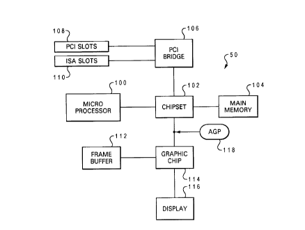
With reference now to the figures, and in particular with reference to Figure
1, a block
AUS9-1997-754 3
CA 02285878 1999-10-15
diagram of a data processing system in which a preferred embodiment of the
present invention may
be implemented is depicted. The data processing system 50 may be, for example,
an RS/6000TM
system, a product of IBM Corporation of Armonk, New York. Data processing
system 50 thus
includes microprocessor 100 and main memory 104 connected operatively to each
other through a
chipset 102. Also connected to chipset 102 is a host bridge ("PCI Host
Bridge") 106, which provides
an interface between chipset 102 and PCI slots 108. Additionally, the host
bridge 106 provides a
similar interface between chipset 102 and ISA slots 110 assuming a PCI to ISA
bridge is included.
PCI slots 106 and ISA slots 110 provide connections for peripheral devices not
shown.
Connected to chipset 102 is a graphic chip 114, which provides the logic and
interface
between a video display or monitor 116 and chipset 102. As shown in Figure 1,
an accelerated
graphic port 118 connects the graphic chip 118 directly to the chipset 102.
The design of the
accelerated graphics port 118 gives the graphics chip 114 of the data
processing system 50 the same
direct connection with the chipset 102 as honors the microprocessor 100, PCI
bridge 106 and main
memory 104. It should be noted that the accelerated graphics port 118 operates
solely between two
devices. To the accelerated graphic port 118 system, the chipset 102 is the
target device and the
accelerated graphic port 118 transfers are controlled by the graphics chip 114
at the other end of the
connection, which is the master when doing AGP transactions. The accelerated
graphic port 118
provides a fast channel for moving large blocks of data between a dedicated
frame buffer 112 and
main system memory 104. The system typically uses direct memory access
transfers across the
2 0 accelerated graphic port 118 to move bit image data from the system memory
104 to the frame buffer
112. In accordance with a preferred embodiment of the present invention, at
least one graphic chip
and chipset pair depicted in Figure 1 implements an enhanced AGP bus
architecture. Functional
operations, such as pipelined memory and having separate address and data
lines, of the accelerated
graphic port 118 architecture are also supported. The enhanced accelerated
graphic port 118
2 5 architecture supports a 32 bit Address/Data bus, and may support a 64 bit
Address/Data bus if the
pin count for such support can be provided.
While supporting much of the existing accelerated graphic port 118
architecture protocols,
the enhanced accelerated graphic port 118 architecture employs differential
signaling between the
chipset 102 and graphics chip 114. Thus, two signal lines are required for
each signal in the
AUS9-1997-754
CA 02285878 1999-10-15
enhanced accelerated graphic port 118 architecture. Therefore, in accordance
with a preferred
embodiment of the present invention, a new connector for the enhanced
accelerated graphic port
architecture must also be defined. Adding the differential signaling
environment should be
transparent to the accelerated graphic port protocol, and an increased
frequency may be achieved,
scalable up to a maximum frequency dependent on the driver/receiver technology
selected. When
operating at a significantly higher frequency, accelerated graphic port timing
requirements must be
adjusted based on the driver/receiver technology employed and actual maximum
frequency selected.
Referring to Figures 2A and 2B, comparative diagrams of signal lines on a
backplane or
adapter card within a data processing system are illustrated. Figure 2A
illustrates the effect of
employing conventional signal lines. Conventional single-ended signal
detection currently
employed by the accelerated graphic port architecture requires detection of a
signal level (high or
low) with respect to ground. Capacitive cross-coupling between the signal
lines 202 and 204 and
ground 206 results in electromagnetic field 208. Energy is thus expended
during transfer of
information on the bus for charging and discharging bus capacitances. Signal
lines may also
cross-couple or interfere between each other, creating noise problems.
Figure 2B illustrates a signal line pair arrangement for a backplane or
adapter card within
an enhanced accelerated graphic port in accordance with a preferred embodiment
of the present
invention. The signal line arrangement illustrated is applicable to
accelerated graphic port based
systems as well as to other systems. Rather than conventional single-ended
signal lines presently
2 0 used in accelerated graphic port architectures, differential signal line
pairs 210a-210b and 212a-212b
are employed. A differential signal requires two lines per signal, and
information is transferred by
detecting either a polarity or a magnitude of a voltage difference between the
two signal lines.
Signal line pairs 210a-210b and 212a-212b preferably transmit signals which
are equal in
magnitude but opposite in polarity. That is, if signal line 210a carries a
signal of +1 V, signal line
2 5 210b simultaneously carries a signal of-1 V. As a result, the
electromagnetic field between a signal
line pair, such as signal line pair 210a-210b, and ground 206 is negligible,
since the electromagnetic
field between one signal line 210a and ground 206 cancels the electromagnetic
field between the
other signal line 210b and ground 206. Only the electromagnetic field 214
between signal lines in
a signal line pair--between signal lines 210a and 210b, for example--remains
significant. As shown,
AUS9-1997-754
CA 02285878 1999-10-15
the electromagnetic field formed between differential signal lines in a signal
line pair is much
smaller and more localized than the electromagnetic field between a
conventional single-ended
signal line and ground. Therefore, when compared to the conventional signaling
environment, a
much lower signal transition is required to transfer information. Less energy
is expended on the bus
charging and discharging capacitance during transfer of information. Moreover,
utilizing differential
signaling improves noise immunity and allows higher transfer rates to be
achieved. As much as
possible, each of the differential signal line pairs 210a-210b and 212a-212b
are routed together in
close proximity with each other on the mother board and add-in adapter board
employed in the data
processing system. This assures that the differential signaling benefits--the
canceling effect of
cross-coupling between signal lines and ground or other signal lines--are
realized between the
chipset and the graphic chip.
With reference to Figures 3A and 3B, comparative diagrams ofpin layouts for an
accelerated
graphic port connector within a data processing system are depicted. Figure 3A
depicts a
conventional signal pin arrangement. The electromagnetic field 302 between
signal pins 304 and
306 and ground pins 308 may be substantial, as shown. Figure 3B depicts a
differential signal pair
arrangement for an enhanced accelerated graphic port in accordance with a
preferred embodiment
of the present invention. The connector pin arrangement depicted would be
applicable to accelerated
graphic port-based systems as well as to other systems. To take advantage of
the benefits of
differential signaling and for signal quality, each of the two pins forming a
differential pair are
2 0 placed adjacent to each other in the connector. Similar to the signal line
arrangement in Figure 2B,
the electromagnetic field 310 between signal pin pairs 312a-312b and 314a-314b
is much smaller
and more localized than found in connectors using conventional signal pin
arrangement for
accelerated graphic port connections.
Referring to Figure 4, a block diagram of a bi-directional signaling net for
an enhanced
2 5 accelerated graphic port utilizing differential signaling in accordance
with a preferred embodiment
of the present invention is illustrated. This type of signaling net may be
employed for all
Address/Data signal lines in an enhanced accelerated graphic port which
require bi-directional
capability. Signaling net 402 receives and transmits at an input/output 404 a
single-ended signal
from an enhanced accelerated graphic port master and/or target (not shown).
The bus master may
AUS9-1997-754
CA 02285878 1999-10-15
be a graphics board or any other graphic chip capable of acting as an
accelerated graphic port bus
master. Signaling net 407 transmits and receives a single-ended signal from an
enhanced accelerated
graphic port master and/or target (not shown) at input/output 406. The bus
target in accordance with
the present invention is typically the chipset for AGP transactions. Both the
bus master and the bus
target according to the invention utilize the enhanced accelerated graphic
port definition.
Input 404 is connected to single-ended-to-differential driver 408 associated
with the
accelerated graphic port master and/or target, which converts the single-ended
signal to a differential
signal in accordance with methods known in the art. Driver 408 transmits the
differential signal on
differential signal line pair 410a-410b. The differential signal transmitted
may indicate different
states in a variety of manners. For example, two different states may be
defined by a voltage
difference on differential signal line pair 410a-410b which remains constant
in magnitude but
changes direction, such as when the polarity of the voltage difference is
reversed. A first polarity
may represent a first state ("high") while the opposite polarity represents a
second state ("low").
Alternatively, the voltage difference on differential signal line pair 410a-
410b may remain constant
in direction or polarity, but change magnitude in opposite directions, with a
first magnitude
representing a first state and a second magnitude representing a second state.
In either case,
however, the voltages applied to differential signal line pair 410a-410b
should have the same
magnitude change but opposite directions with respect to ground, so that the
canceling effect may
be achieved.
2 0 Differential signal line pair 410a-410b is also connected to receiver 412
associated with the
accelerated graphic port master and/or target, which transforms the
differential signal to a
single-ended signal by methods known in the art. The resulting single-ended
signal is transmitted
on output 406 to the accelerated graphic port master and/or target. Since bi-
directional signaling is
required for this example, a second driver 414 associated with the accelerated
graphic port target is
2 5 connected to output 406 and differential signal line pair 410a-410b.
Driver 414 receives
single-ended signals at output 406 from the accelerated graphic port target
and transmits
corresponding differential signal on differential signal line pair 410a-410b.
A receiver 416
associated with the accelerated graphic port master is connected to
differential signal line pair
410a-410b and input 404, transforming differential signals received to single-
ended signals and
AUS9-1997-754
CA 02285878 1999-10-15
transmitting the single-ended signals to the accelerated graphic port master.
Drivers 408 and 414
and receivers 412 and 416 each include an enable signal input, preventing the
respective devices
from transmitting or receiving unless asserted. The signals applied to these
enable signal inputs are
coordinated to ensure that only one driver is transmitting during a given bus
cycle.
In addition to cross-coupling, an additional problem with the conventional
single-ended
signal lines employed in existing accelerated graphic port architectures is
reflective signaling.
Employing balanced loads on the signal lines eliminates reflections and
results in single incident
signaling. Therefore, each transceiver 418 and 420 comprising a
driver/receiver pair associated with
either a accelerated graphic port master or target includes a resistive load
at the connection to
differential signal line pair 410a-410b. The resistive load comprises
resistance R1 connected
between an upper power supply voltage and one differential signal line 410a,
resistance R2
connected between and lower power supply voltage and the other differential
signal line 410b, and
resistance R3 connected between the differential signal lines 410a and 410b.
The values of R1, R2,
and R3 are selected to ensure that the loads seen by differential signal line
pair 410a-410b remains
substantially balanced and constant regardless of which transceiver 418 or 420
is transmitting and
which is receiving.
The driver/receiver pair 408 and 416 optimally would be within the accelerated
graphic port,
and driver/receiver pair 412 and 414 would optimally be within a accelerated
graphic port interface
chip such as on a graphic chip. Termination resistors Rl, R2, and R3 in
transceiver 418 would be
2 0 located on the motherboard, close to the accelerated graphic port in this
example. Resistor network
R1, R2, and R3 in transceiver 420 would also be on the motherboard located at
the end of the
accelerated graphic port.
With reference to Figure 5, a block diagram of an alternative signaling net
for an enhanced
accelerated graphic port utilizing differential signaling in accordance with a
preferred embodiment
of the present invention is depicted. This simpler signaling net may be
employed for signal lines
which do not require bi-directional capability. Signaling net 502 receives
single-ended signals from
a bus master (not shown) at input 504 connected to driver 506. Driver 506
transforms the
single-ended signals to differential signals and transmits the differential
signals on differential signal
line pair 508a-508b. Receiver 510 connected to differential signal line pair
508a-508b transforms
AUS9-1997-754 g
CA 02285878 1999-10-15
the differential signals to single-ended signals and transmits the single-
ended signals on output 512
to a bus master and/or target (not shown).
Resistive loads associated with both driver 506 and receiver 510 ensure that
differential
signal line pair 508a-508b is connected to a balanced load. This is
accomplished at driver 506 by
resistance Ra connected between an upper power supply voltage and differential
signal line 508a,
resistance Rb connected between a lower power supply voltage and differential
signal line 508b, and
resistance R~ connected between differential signal lines 508a and 508b. A
similar resistive load
configuration is associated with receiver 510, although providing a balanced
load at receiver 510
may require that different resistance values RX, Ry, and RZ be employed.
As described above, this invention defines a means to take the date transfer
rate of the current
accelerated graphic port connection to significantly higher levels. This is
accomplished by defining
a new connector similar to the accelerated graphic port connector, and
changing it to a differential
signalling arrangement. This requires the addition of an additional signal pin
for each existing signal
pin, to allow differential signal pairs. This change utilizes the same
accelerated graphic port and PCI
protocols as defined in the accelerated graphic port specification, but
utilizes differential signalling
instead of the traditional single ended signalling.
While the invention has been particularly shown and described with reference
to a preferred
embodiment, it will be understood by those skilled in the art that various
changes in form and detail
may be made therein without departing from the spirit and scope of the
invention.
AUS9-1997-754