Note: Descriptions are shown in the official language in which they were submitted.
' CA 02286231 1999-10-13
\LCH\197-1348
METHOD FOR SOLDERING DPAK-TYPE ELECTRONIC COMPONENTS
TO CIRCUIT HOARDS
BACKGROUND OF THE INVENTION
1. Field of the Invention
The present invention relates generally to soldering
l0 electronic components to circuit boards, and more
particularly to a method for soldering DPAK-type electronic
components to circuit boards.
2. Disclosure Information
DPAKs are relatively high-power electronic switching
devices (e.g., transistors) that are commonly used on
circuit boards. As illustrated in FIGS. 1A-C, a typical
DPAK 10 includes an integrated circuit die 12 attached atop
a heatspreader 14, with one or more selected sites on the
top surface of the die wirebonded 16 to a like number of
leads 18, and with a plastic or ceramic molded housing 20
encasing the die 12, the wirebond wires 16, a portion of
the leads) 18, and a portion of the heatspreader 14.
A typical DPAK has two leads 18, but other DPAK-type
components 10 may have one lead (e. g., a diode), three
leads, and so forth. Typically the heatspreader 14 itself
serves as an electrical interconnect, such as in transistor
DPAKs where the heatspreader 14 is electrically connected
to the base of the transistor die 12. (Usually the bottom
surface of a transistor die serves as the base interconnect
point, with the emitter and collector interconnect points
being situated on the top surface of the die.)
As illustrated in FIG. 1B, DPAK-type components 10 are
electrically and mechanically connected to circuit boards
30 by applying solder paste 36 to the heatspreader/lead
mounting pads 32/34, positioning the component 10 with its
__ 1 __
CA 02286231 1999-10-13
heatspreader 14 and leads 18 resting atop their respective
solderrpasted pads 32/34, and sending the component/board
combination through a conventional reflow oven. For most
types of electronic components, reflow soldering is an
efficient and effective way of forming robust solder joints
connecting a component's leads/terminations/etc. to their
corresponding mounting pads.
However, conventional reflow soldering is not as
effective at forming robust solder joints on DPAK-type
components 10. Because the heatspreader 14 of a DPAK-type
component is so large, it is often difficult to provide
enough thermal energy to such components during reflow to
melt all of the solder paste 36 sandwiched between the
heatspreader 14 and its mounting pad 32. One approach for
alleviating this problem is to simply increase the reflow
oven peak temperature and/or increase the circuit board's
exposure time to the peak temperature, but this approach
has the drawback of risking damage to other components
and/or to the substrate. Another approach is to use a
laser rather than a reflow oven to solder the components.
In laser soldering, a laser beam is directed at the
component leads, terminations, exposed heatspreader
portion, and/or the heatspreader mounting pad 32, so as to
melt the solder paste 36 on the pad 32. However, as with
reflow soldering, the heatspreader 14 of a DPAK-type
component 10 is often too large to permit robust solder
joint formation, even if a high laser power setting and
long lase time are used.
In both of the foregoing approaches, it is often the
case that the solder paste 36 immediately adjacent the
exposed portion 14e of the heatspreader is the only portion
thereof that gets melted. This results in a solder joint
that forms only proximate the exposed portion 14e of the
heatspreader, with no joint being formed underneath the
component.
__ 2 __
CA 02286231 1999-10-13
It would be desirable, therefore, to provide a way of
soldering DPAK-type components to circuit boards without
the aforementioned drawbacks.
SUMMARY OF THE INVENTION
The present invention overcomes the disadvantages of
the prior art approaches by providing a method for
soldering an electronic component having a heatspreader on
a bottom surface thereof and at least one lead (e.g., a
DPAK-type component) to a circuit board having a
heatspreader mounting pad and at least one lead mounting
pad, comprising the steps of: (a) depositing solder paste
on the heatspreader mounting pad and on each of the at
least one lead mounting pad; (b) placing the electronic
component on the circuit board such that the heatspreader
rests atop the heatspreader mounting pad and each lead
rests atop a respective one of the at least one lead
mounting pad; (c) directing a laser energy beam from a
diode laser at the heatspreader and/or heatspreader pad for
a first predetermined length of time, thereby heating the
solder paste on the heatspreader mounting pad; and (d)
continuing to direct the laser energy beam at the
heatspreader and/or heatspreader pad for a second
predetermined length of time while simultaneously feeding a
predetermined amount of flux-core wire solder into the
laser energy beam proximate the heatspreader, such that the
wire solder melts and flows onto at least one of the
heatspreader and the heatspreader mounting pad.
It is an object and advantage that the method of the
present invention is effective at forming robust solder
joints on DPAK-type electronic components.
Another advantage is that the method of the present
invention may be used with low-melting-point substrate
materials that cannot be exposed to the temperature
profiles of conventional reflow soldering.
__ 3 __
CA 02286231 1999-10-13
Yet another advantage is that the present invention
may be, easily utilized in conjunction with conventional
laser soldering.
These and other advantages, features and objects of
the invention will become apparent from the drawings,
detailed description and claims which follow.
BRIEF DESCRIPTION OF THE DRAWINGS
FIGS. 1A-C are top, side section, and perspective
views, respectively, of a typical DPAK electronic
component.
FIG. 2 is a perspective view of an unpackaged bare die
on a heatspreader.
FIG. 3 is a side view of a DPAK-type electronic
component being soldered to a circuit board using a diode
laser beam and flux-core wire feed according to the present
invention.
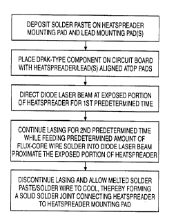
FIG. 4 is a schematic flowchart of the process steps
of the present invention.
DETAILED DESCRIPTION OF THE PREFERRED EMBODIMENTS
Referring now to the drawings, FIGS. 3-4 illustrate a
method for soldering an electronic component 10 having a
heatspreader 14 on a bottom surface thereof and at least
one lead 18 (e. g., a DPAK-type component) to a circuit
board 30 having a heatspreader mounting pad 32 and at least
one lead mounting pad 34. The method comprises the steps
of: (a) depositing solder paste 36 on the heatspreader
mounting pad 32 and on each of the at least one lead
mounting pad 34; (b) placing the electronic component 10 on
the circuit board 30 such that the heatspreader 14 rests
atop the heatspreader mounting pad 32 and each lead 18
rests atop a respective one of the at least one lead
__ 4 __
___ _. ._ _._ __ _.____._
CA 02286231 1999-10-13
mounting pad 34; (c) directing a laser energy beam 42 from
a diode laser 40 at the heatspreader 14 and/or heatspreader
pad 32 for a first predetermined length of time, thereby
heating the solder paste 36 on the heatspreader mounting
pad 32; and (d) continuing to direct the laser energy beam
42 at the heatspreader/pad 14/32 for a second predetermined
length of time while simultaneously feeding a predetermined
amount of flux-core wire solder 50 into the laser energy
beam 42 proximate the heatspreader 14, such that the wire
l0 solder 50 melts and flows onto at least one of the
heatspreader 14 and the heatspreader mounting pad 32.
To assist the reader in understanding the present
invention, all reference numbers used herein are summarized
in the table below, along with the elements they represent:
10 - DPAK-type electronic component
12 - Integrated circuit die
14 - Heatspreader
14e = Exposed portion of heatspreader
16 - Wirebond wire
18 - Lead
20 - Molded housing
- Circuit board
25 32 - Heatspreader mounting pad
34 - Lead mounting pad
36 - Solder paste
38 - Circuit trace
- Diode laser
30 42 - Laser energy beam from diode laser
- Flux-core solder wire
The electronic component 10 may be a DPAK, D2PAK,
D3PAK, or any other DPAK-type component. As used herein, a
35 "DPAK-type electronic component" includes any electronic
component 10 which has a heatspreader 14 on a bottom
surface thereof with the heatspreader being visible from
above the component 10 when the component is situated on
its respective mounting pads 32/34 on a circuit board 30.
__ 5 -_
CA 02286231 1999-10-13
An example of such a component 10 is a common unpackaged
bare die 12 that is bonded to a heatsink 14 and soldered to
a circuit board mounting pad 32, whereupon one or more
(typically two) sites on the top die surface are wirebonded
16 to bond pads on the circuit board, as illustrated in
FIG. 2. (This is essentially the same construction as a
common DPAK, but without the plastic/ceramic housing 20 and
with wirebond wires 16 wirebonded directly to the mounting
pads 34 rather than being wirebonded to an intermediary
leadframe 18.)
The circuit board 30 may be a rigid laminated polymer
substrate (e. g., FR-4), a semi-rigid to rigid molded
polymer substrate, a flexible polymer substrate (e. g.,
polyester), an etched tri-layer metallic circuit containing
air bridges, or the like. The mounting pads 32/34 and
circuit traces 38 may be applied using a traditional
photoimaging, plating, and etching approach, or may be
sputtered, vacuum deposited, or otherwise applied. As
mentioned above, one advantage of the present invention is
that the processing temperature to which the circuit board
is exposed is much lower than with conventional reflow or
laser soldering temperatures, thus permitting the use of
low-melting-point polymers as the circuit board substrate
material.
It is desirable to use a diode laser 40 as the energy
source rather than other types of lasers (e. g., Nd:YAG)
because of the 800-1000 nm frequency range of the laser
beam 42 produced. Energy in this wavelength is readily
absorbed by metals -- such as the heatspreader 14, the
heatspreader mounting pad 32, and the solder balls in the
solder paste -- but is not readily absorbed by most
polymeric materials -- such as the materials most commonly
used to produce circuit board substrates 30 -- thus making
the diode laser 40 a preferred energy source for electronic
component soldering.
-_ 6 --
CA 02286231 1999-10-13
Once the solder paste 36 is deposited on the pads
32/34 and the component 10 has been positioned thereon, the
laser energy beam 42 is directed at the exposed
heatspreader portion 14e and/or at the heatspreader pad 32
for a first predetermined time. This time is calculated so
as to be long enough to heat the solder paste 36 proximate
the exposed heatspreader portion 14e to a temperature
generally between the melting point of the solder paste and
about 225°C. For example, for common eutectic tin-lead
l0 solder paste, this range would be generally between 183QC
and 225qC, and for a common DPAK component the first
predetermined time would be about 7 seconds. Next, the
beam 42 would continue to be directed at the exposed
heatspreader portion and/or pad 14e/32 for a second
predetermined time, while simultaneously feeding a
predetermined length or amount of flux-core wire solder 50
into the beam 42 adjacent the exposed heatspreader portion
14e. This second predetermined time should be long enough
to heat the solder paste 36 sandwiched between the
heatspreader 14 and its mounting pad 32 to a temperature
generally between about 200°C and 240°C. For the example
above, this second predetermined time would be about 5
seconds in duration.
Feeding the wire solder 50 into the beam 42 causes the
wire solder to melt into liquid solder (e. g., molten tin-
lead alloy) and liquid flux. It has been observed that the
liquid solder tends to remain proximate the exposed
heatspreader portion 14e (i.e., proximate the area where it
was melted by the diode laser beam 42), while the liquid
flux tends to quickly flow away from the exposed
heatspreader portion 14e and underneath the rest of the
heatspreader 14. This causes the heat to be given up by
the hot liquid flux to the not-yet-melted solder paste 36
underneath the heatspreader 14, thereby urging the solder
paste thereat to melt. Once the second predetermined time
has elapsed, the laser beam 42 is turned off and the melted
solder paste 36 and melted wire solder 50 are allowed to
cool, thereby forming a solder joint connecting the
__
CA 02286231 1999-10-13
heatspreader 14 to its mounting pad 32. Tests using the
present method have indicated that substantially the entire
bottom surface of the heatspreader 14 becomes soldered to
the heatspreader mounting pad 32, with a robust
metallurgical bond being formed therebetween. This
represents a significant improvement over the prior art
approaches for soldering DPAK-type components.
Another advantage of the present method is that
commonly available flux-core wire solder may be used.
Typical flux-core solder includes about 2 to 4~ flux with
the balance being solder metal. Typical diameters for such
wire solder range from about 0.015 to 0.030 inches. The
rate of wire feed for a common DPAK may range from about 1
IS to 25 mm/sec, with a typical solder wire volume of about 2
to 36 mm3. For most applications, a diode laser power
setting of 5 to 45 Watts is sufficient.
Various other modifications to the present invention
may occur to those skilled in the art to which the present
invention pertains. Other modifications not explicitly
mentioned herein are also possible and within the scope of
the present invention. It is the following claims,
including all equivalents, which define the scope of the
present invention.
__ g __