Note: Descriptions are shown in the official language in which they were submitted.
CA 02286246 1999-10-06 '
w
-1- PCT/LJS 98/0693 3
METHODS OF FORMING OPTICAL RODS INCLUDING THREE
DIMENSIONAL PATTERNS ON END FACES THEREOF
The U.S. Government may have rights to the present invention under government
contract'~lo. N00178-97-C-3058 issued by the Naval Surface Warfare Center.
Related Applications
The present application claims priority based on Provisional Application
Serial
No. 60/043,28, filed April 11, 1997, entitled "Wafer Processing of Multiple
Glass Rods
. For Incorporating Optical Elements On The Ends Thereof', the disclosure of
which is
hereby incorporated herein in its entirety by io reference. The present
application is also
related to U.S. Patent Application Serial No. 08/991,803 entitled "Optical
Rods With
Three-Dimensional Patterns Thereon And Related Structures" filed concurrently
herewith. the disclosure of which is hereby incorporated herein in its
entirety by
reference.
Field of the Invention
1 ~ The present invention relates to the field of optics and more particularly
to
methods of forming optical structures.
(! Background of the Invention
Single mode fiber optic data links have been developed as alternatives to
multimode fiber data links. In a single mode fiber, a single spatial mode
propagates
therethrough so that modal noise effects are reduced. Single mode optical
systems,
however, may be extremely sensitive to alignment errors. Sensitivity to
alignment errors
may be particularly critical when a data link is used in an extreme
environment with
exposure to vibrations and shock. A need thus exists to provide single mode
fiber optic
connections ~~hich have reduced sensitivity to shocks and vibrations. Dust and
debris
may also be problematic in single mode fiber connections known in the prior
art.
A single mode fiber optic connection according to the prior art is illustrated
in
AMENDED SHEETS
CA 02286246 1999-10-06 '
a
-2- PCT/LJS98/06933
Figures I and 2. As shown, two single mode optical fibers 11 are inserted into
ferrules 13
that are held together with a spring loaded stainless steel jacket 15. The
springs keep the
ferrules in compression in an attempt to keep the ferrules in contact at all
times. A
ceramic sleeve 17 surrounds the ferrules to keep the ferrules and the fibers
aligned in the
transverse direction. This sleeve is thus precisely machined to tolerances
within 1 micron
on the inner diameter. Accordingly, as light is transmitted from a first one
of the fibers
across the junction to the second fiber, residual losses may occur.
The females, however, may piston in and out of the sleeve as a result of
severe
shocks and/or vibrations thereby creating a gap between the two fibers 11.
This gap may
l-'10 increase optical losses beyond acceptable levels. Moreover, a single
dust particle between
the respective core portions of the two optical fibers may block a significant
portion of the
radiation being transmitted therebetween.
Gradient Index (GRID lenses have been used to collimate and focus light in
fiber
switching and connecting systems. GRIN lenses, however, may be quite large in
comparison with the dimensions of optical fibers thus increasing overall
package sizes
and reducing switching densities. GRIN lenses may also be limited to simple
optical
focusing and collimation functions while current broadband networks may
require
complex functions for Wavelength Division Multiplexing (WDM).
European Patent Application 0256810 teaches patterning an optical rod to form
a
(- 20 phase plate or a zone plate. European Patent Application 0627641 teaches
forming an
array of lens tipped rods using the difference in etch times for the clad and
core material.
U.S. Patent No. 4,761,062 teaches providing an array of rods with a layer of
material over
the rods. None of these disclose simultaneously processing a plurality of rods
including
cutting the rods to form wafers and separating the rods in a wafer after such
processing.
AMENDED SHEETS
CA 02286246 1999-10-06
WO 98/470x5 PCT/US98/06933
-3-
Accordingly, there continues to exist a need in the art for improved
methods and structures for joining two optical fibers to reduce optical losses
for
signals transmitted therebetween.
s Summer of the Invention
It is therefore an object of the present invention to provide methods
of forming improved optic structures.
It is another object of the present invention to provide improved
methods of forming optical beam shaping structures.
io It is still another object of the present invention to provide methods
of forming improved optical rods.
These and other objects are provided according to the present
invention by methods including the steps of bonding a plurality of optical
rods into
an array wherein each of the optical rods is aligned, preferably in parallel,
so that
is an exposed end face of each of the optical rods is oriented in a common
direction. The exposed end faces of the optical rods are patterned so that
each
of the exposed faces has a three-dimensional pattern formed thereon. A large
number of optical rods can thus be patterned simultaneously using
photolithographic mask and etch steps. Moreover, the patterned optical rods
can
2o be separated from the array to provide a plurality of individual patterned
optical
rods. These individual optical rods can then be used in the fabrication of
various
fiber optic systems and micro-optic systems.
More particularly, each of the optical rods can be a glass rod, and
the three-dimensional patterns can be diffractive optical patterns, refractive
2s optical patterns, and/or patterned layers. These various optical patterns
can be
used to provide beam shaping functions, pattern generation functions,
diffusion
functions, collimating functions, focusing functions, andlor wavelength
division
multiplexing functions.
The plurality of optical rods can be bonded into a closely packed
3o array using an epoxy. Alternately, a plurality of parallel grooves can be
formed
on the surface of a first substrate, the optical rods can be arranged in the
grooves, and a second substrate can be bonded onto the surface of the first
substrate so that the optical rods are in the parallel grooves between the
first and
second substrates. Moreover, the grooves can be V-grooves formed by etching
CA 02286246 1999-10-06
WO 98/47045 PCT/US98/06933
a silicon substrate. According to another alternative, the plurality of
optical rods
are bonded into an array within an outer cylinder. In either case, one end of
each
of the plurality of optical rods can be simultaneously patterned.
The step of bonding the plurality of optical rods can include the
s steps of bonding a plurality of optical fibers into an array and cutting the
array of
optical fibers along a direction perpendicular to the axis of each of the
optical
fibers thereby exposing the end faces of each of the optical rods.
Accordingly, a
plurality of arrays of optical rods can be cut from a single an-ay of optical
fibers.
Moreover, optical rod arrays cut from approximately the same portion of the
io optical fiber array will have substantially the same orientation of optical
rod faces.
A common mask set can thus be used to pattern multiple arrays of optical rods
cut from adjacent portions of the original fiber array.
The methods of the present invention can thus be used to provide a
plurality of patterned opticat rods each having a width (or diameter) of 1 mm
or
is less and a length of 6mm or less. Accordingly, the methods of the present
invention can be used to pattern GRIN lenses having widths (or diameters), for
example, of 500 microns or 250 microns, and to pattern glass rods having
diameters of 125 microns which would be dimensionally compatible with the
conventional optical fibers. These precisely patterned micro-optical rods can
thus
2o be used in the fabrication of fiber optic and micro-optic systems. More
particularly, diffractive patterns, refractive patterns, and reflective
patterns can be
provided on end faces of the micro-optic rods of the present invention.
2s Figure 1 is a cross sectional view of an fiber optic connector
according to the prior art.
Figure 2 is a greatly enlarged cross sectional view of the sleeve,
ferrules, and optical fbers of Figure 1.
Figure 3a is a cross sectional view of an expanded beam fiber optic
3o connector including a glass rod formed according to the present invention.
Figure 3b is an enlarged cross sectional view of a glass rod of
Figure 3a.
Figure 4 is an photograph of a patterned end of a glass rod formed
according to the present invention.
CA 02286246 1999-10-06
WO 98/47045 PCT/US98/06933
-5-
Figure 5 is a graph illustrating connector losses as a function of
longitudinal separation for a butt coupled fiber optic connector (circles)
according
to the prior art and for an expanded beam fiber optic connector (squares)
including glass rods formed according to the present invention.
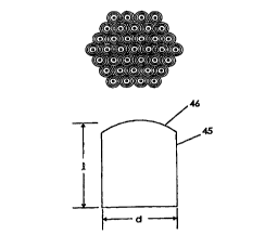
Figure fi is an end view of a bonded fiber array formed according to
the present invention.
Figure 7 is a mask pattern used to form a diffractive pattern on a
glass rod according to the present invention.
Figures 8a-8f are cross sectional views illustrating steps used to
io form a diffractive pattern on a glass rod according to the present
invention.
Figure 9a is a block diagram of a system used to generate
photolithographic masks for a wafer of bonded optical rods according to the
present invention.
Figure 9b is a photolithographic mask formed using the system of
is Figure 9a.
Figure 10a is a cross-sectional view of an optical rod including a
diffractive pattern formed according to the present invention.
Figure 10b is a cross-sectional view of an optical rod including a
refractive pattern formed according to the present invention.
2o Figure 10c is a cross-sectional view of an optical rod including a
pattern formed according to the present invention.
Figure 11 is a cross sectional view illustrating an array of optical
fibers arranged in V-grooves formed according to the present invention.
Figures 12a and 12b are cross sectional views illustrating steps
2s used to form V-grooves in a substrate according to Figure 11.
Figure 13 is a cross sectional view illustrating a stacked array of
substrates including V-grooves and optical fibers formed according to the
present
invention.
3o Detailed De ri tion
The present invention v~ill now be described more fully hereinafter
with reference to the accompanying drawings, in which preferred embodiments of
the invention are shown. This invention may, however, be embodied in many
different forms and should not be construed as limited to the embodiments set
CA 02286246 1999-10-06
WO 98/47045 PCT/US98/06933
-6-
forth herein; rather, these embodiments are provided so that this disclosure
will
be thorough and complete, and will fully convey the scope of the invention to
those skilled in the art. In the drawings, the dimensions of elements are
exaggerated for clarity. Like numbers refer to like elements throughout. It
will
also be understood that when an element is referred to as being "on" another
element, it can be directly on the other element, or intervening elements may
also
be present.
An optical fiber connector including an optical rod formed according
to the present invention is illustrated in Figures 3a and 3b. As shown, two
optical
io fibers 21a and 21b are inserted into respective ferrules 23a and 23b which
are
aligned within the sleeve 25 as before. In addition, the glass rods 27a and
27b
are provided at the ends of the respective optical fibers within the ferrules.
As
shown in Figure 3b, an epoxy 29 can be used to bond the glass rod 27a to the
end of the optical fiber 21 a, and a three dimensional pattern 31 a can be
provided
~s on the end of the glass rod 27a opposite the optical fiber 21a. In
particular, the
three-dimensional pattern 31a can be used to provide a diffractive lens or a
refractive lens on the end of the glass rod. Similarly, an epoxy can be used
to
bond the optical fiber 21 b and the glass rod 27b, and a three-dimensional
pattern
31 b can be provided on the end of the glass rod 27b opposite the optical
fiber
20 21 b.
The glass rods 27a and 27b can each be provided with a diffractive
lens as discussed above to reduce optical losses for light transmitted between
the two optical fibers 21 a and 21 b. The operation of the glass rods will now
be
discussed with reference to Figure 3a for light being transmitted from the
first
2s optical fiber 21 a to the second optical fiber 21 b. Light is generally
transmitted
through the central core region of an optical fiber. Accordingly, fight
transmitted
through the first optical fiber 21a will expand as it passes through the glass
rod
27a which has a uniform index of refraction across its diameter. The
diffractive
lens 31 a can thus be used to collimate the expanded beam. The diffractive
lens
30 31 b on the second glass rod 27b can then be used to focus the expanded and
collimated beam into the core of the second optical fiber 21 b. The end face
of a
glass rod with a diffractive lens patterned thereon is illustrated in Figure
4. In
particular, the diffractive lens of Figure 4 is an eight phase-level
diffractive pattern
etched onto a 125 micron diameter glass rod. This micro-optical rod can thus
fit
CA 02286246 1999-10-06
WO 98/47045 PGT/US98/06933
_7_
snugly into a standard ferrule to provide an expanded beam optical fiber
connection having coupling effciencies with losses of less than 1 dB and
having
a high degree of collimation.
The sensitivity to vibrations and shocks can thus be reduced so that
s the expanded and collimated beam can traverse varying gaps between the glass
rods with reduced optical losses. As shown in Figure 5, the optical losses
with
respect to displacement are relatively invariant for expanded beam connectors.
As further shown in Figure 5, the optical losses increase rapidly with
increasing
displacements in conventional connectors. In other words, the performance of
io the conventional connector degrades rapidly as a function of separation
distance.
Furthermore, a single dust particle between the two optical rods may block
only a
small portion of the expanded beam of fight transmitted therebetween thus
reducing the losses due to dust.
Diffractive lenses can be used instead of the refractive ball lenses
is of the prior art. Diffractive lenses have the advantages of reduced
birefringence
and/or aberration effects because diffractive lenses can provide nearly
perfect
lens functions when patterned onto the rods.
A method of mass producing optical rods including the patterned
end faces according to the present invention will now be discussed with
reference
2o to Figures 6-9. As an example, a plurality of optical fibers such as glass
fibers
each having a diameter of approximately 125 microns can be arranged into a
closely packed array and bonded with an epoxy which can be UV cured or
thermally cured. The array of fibers can then be diced (or cut) into a
plurality of
wafers wherein each wafer has a thickness of approximately 1 mm. Accordingly,
2s each of the wafers can include a plurality of glass rods aligned in
parallel and
bonded together with the epoxy wherein each glass rod has a diameter of
approximately 125 microns and a length of approximately 1 mm. Each wafer
thus has two opposing faces, and one end face of each of the glass rods is
exposed at each wafer face so that one end face of each of the glass rods can
be
3o patterned with a three-dimensional pattern simultaneously. The epoxy can
then
be chemically dissolved thereby separating each of the patterned glass rods
for
assembly into fiber optic connectors or other optical applications.
CA 02286246 1999-10-06
WO 98/47045 PCT/US98/06933
-8-
As shown in Figure 6, nineteen closely packed optical fibers can be
surrounded by a glass sleeve and bonded with an epoxy. Much larger arrays of
fibers having on the order of 1,000 to 20, 000 fibers can also be provided.
Accordingly, a wafer diced from an array will have a number of optical rods
s corresponding to the number of optical fibers in the parent fiber array. The
nineteen fiber array illustrated in Figure 6 has been found to be repeatable,
but
packing errors on the order of 5 microns to 10 microns may occur. The
Applicants theorize that the packing arrangement is a function of the boundary
into which the fibers are inserted.
io By providing a large number of optical rods in a single wafer, the
large number of optical rods can be patterned simultaneously using
photolithographic techniques developed in the microelectronics industry. As an
example, an array of thousands of 125 micron low OH glass fibers can be
bonded together using a UV cured epoxy. This array of fibers can then be diced
is (or cut) to provide a plurality of 1 mm thick wafers with thousands of
optical rods
per wafer. At least one face of each of these wafers is then optically
polished to
facilitate photolithographic patterning. This polishing step is preferably
performed
so that the formation of micro-fractures in the optical rods is reduced. In
particular, a double lapping polisher can be used. Accordingly, each of the
20 optical rod end faces making up the polished wafer face lie in a common
plane so
that each of the polished end faces can be photolithographically patterned
simultaneously.
In particular, one or more photolithographic mask and etching steps
can be used to form diffractive patterns having one or more steps (two or more
2s levels) in the exposed end faces of each of the optical rods. The formation
of
diffractive patterns is discussed for example in U.S. Patent No. 5,218,471
entitled
"High-Efficiency, Multi-Level, Diffractive Optical Elements" to Swanson et
al., the
disclosure of which is hereby incorporated herein in its entirety by
reference. The
formation of a multi-level diffractive pattern will now be briefly discussed
with
3o reference to Figures 7 and 8A-8H. In particular, Figure 7 illustrates a
typical
mask pattern used when forming a diffractive pattern on an end face of an
optical
rod. Multiple masks can be used to create diffractive patterns having up to 2"
levels where n is the number of masks.
CA 02286246 1999-10-06
WO 98/47045 PCT/US98/06933
-9-
The use of two masks to create a four level diffractive pattern is
illustrated in Figures 8A-8F. A first mask 31 is used to pattern a first
photoresist
layer 33 on an end face 35 of an optical rod as shown in Figures 8A and 8B.
The
patterned photoresist layer 33 is used as an etch mask during a reactive ion
etch
s to produce steps in the face 35 of the optical rod, and the first patterned
photoresist layer is then removed as shown in Figure 8C. A second mask 37 is
then used to pattern a second photoresist layer 39 as shown in Figures 8D and
8E. The second patterned photoresist layer 39 is then used as an etch mask
during a second reactive ion etch to produce two additional steps in the face
35,
io and the second patterned photoresist layer is then removed as shown in
Figure
8F. Accordingly, stepped diffractive patterns can be formed with the
resolution
being determined by the number of mask and etch steps used. The height of
each step can be controlled by controlling the duration of the respective
reactive
ion etch.
is In order to simultaneously pattern each of the exposed end faces of
the optical rods in a wafer, each photomask should include a separate masking
pattern corresponding to each of the optical rod end faces, and these separate
masking patterns should be precisely arranged to correspond to the arrangement
of the end faces within a wafer. Because the arrangement of the optical rods
2o may differ from wafer to wafer as a result of packing errors, different
photomask
sets may be needed for different wafers. In other words, a custom mask set may
be needed for a particular wafer of optical rods. Because wafers cut from
adjacent portions of a fiber array may have a substantially identical
arrangement
of optical rods, a custom mask set can be used for as many as ten to twenty
2s wafers diced from a single optical fiber array. Accordingly, a custom mask
set
used to pattern ten to twenty wafers with 10,000 to 20,000 optical rods per
wafer
can yield as many as 150,000 or more patterned optical rods. The production of
custom mask sets can thus be justified economically.
A custom mask set can be generated using an E-beam writing
so technique. In particular, the arrangement of individual patterns on each
mask in
the set should be determined to correspond to the arrangement of the optical
rod
faces to be patterned. An automated system for determining the locations of
each of the optical rod end faces on a wafer of optical rods is illustrated in
Figure
9a. This system includes a computer 41, a camera 43, and a stage 45 for
CA 02286246 1999-10-06
WO 98/47045 -1 O- PCT/US98/06933
analyzing a wafer 47 of optical rods. By scanning the wafer 47 with the camera
43 and providing the information to the computer 41, the x-y coordinates 49 of
the
center points of each of the optical rod end faces can be determined within
micron positional tolerances using the optical instrumentation together with
s pattern recognition and data processing techniques. In other words, pattern
recognition techniques are used to locate the centers of the individual
optical rod
faces as the camera is scanned across the wafer on a micro-stage.
The x-y coordinates are then used to generate the custom mask
set. In particular, a data file including the x-y coordinates locating the
center
io points of the optical rod end faces can be electronically transferred to
mask
generation equipment used to form E-beam written masks. The mask generation
equipment uses the x-y coordinates to layout each mask in the set wherein each
mask includes a plurality of identical mask patterns centered about the
designated x-y coordinates to correspond to the locations of the optical rod
end
is faces. This step is also known as data fracturing. An E-beam is then used
to
direct write to a photoresist layer on a mask blank, and the patterned
photoresist
layer is used as an etch mask to pattern the mask blank. This procedure is
repeated for each mask in the set. An example of a mask thus formed is
illustrated in Figure 9b. While the mask of Figure 9b includes 37 mask
patterns, it
2o will be understood that these principles can be used to fabricate custom
masks
including tens of thousands of mask patterns corresponding to tens of
thousands
of optical rod end faces in a wafer.
The individual optical rod end faces in the wafer are then patterned
using the custom mask set discussed above. In particular, a photoresist layer
is
2s spun on the wafer covering the optical rod end faces. This photoresist
layer is
then exposed and developed using the first mask from the custom mask set
wherein individual mask patterns from the first mask are aligned with
individual
rod end faces. Portions of the rod end faces exposed by the patterned
photoresist layer are etched using a timed reactive ion etch to provide a two
level
3o stepped structure. Additional steps and/or levels can be added to the
structure
by adding additional mask and etch steps to provide diffractive lenses having
higher levels of resolution. Diffractive patterns can thus be used
advantageously
in narrow band communication networks.
CA 02286246 1999-10-06
WO 98/47445 PGT/US98/06933
-11-
As shown in Figure 10a, an optical rod 51 having a length I and a
diameter d can be formed having a three-dimensional diffractive (stepped)
pattern 52 on an end thereof. The optical rod can have a cylindrical shape, a
length I of approximately 6mm or less, and a diameter d of approximately 1 mm
or
less which would have been difficult to produce using prior art techniques.
More
particularly, the optical rod can be a GRIN lens having a diameter, for
example, of
250 microns or 500 microns, or a glass rod having a diameter of 125 microns
which would be dimensionally compatible with conventional optical fibers.
Alternately, refractive lenses can be provided on the rod end faces
io by patterning the photoresist layer so that a circular photoresist pattern
covers
each of the rod end faces, and reflowing the circular photoresist patterns so
that
the photoresist tapers off at the edges of each of the rod end faces. A
reactive
ion etch then etches through the tapered photoresist pattern so that the edges
of
the rod end faces with thinner photoresist thereon are etched for a longer
time
is than central portions of the rod faces with thicker photoresist thereon.
Accordingly, a rounded rod end face can be provided on each of the rods
thereby
providing a refractive lens. The individual circular mask patterns can be laid
out
on the mask using the steps discussed above with regard to the Figure 9.
Refractive lenses can be used advantageously to focus a broad range of optical
2o wavelengths in broadband networks which operate at two or more multiplexed
wavebands. As shown in Figure 10b, the optical rod 54 can have a refractive
(rounded) pattern 55 on an end thereof. Alternately, the rounded resist can
provide the lens without etching. Other methods of forming refractive lenses
are
discussed in Provisional Patent Application Serial No. 60/041,042 entitled
"Gray
2s Mask Made of Absorptive Materials and for Fabricating Optical Elements
Using a
Photoresist Formed From Contact Printing of a Gray Mask" to Feldman et al. and
filed March 21, 1997. The disclosure of this Provisional Application is hereby
incorporated herein in its entirety by reference.
According to another alternative, the wafer end face can be covered
3o with a layer of another material such as a highly reflective dielectric
material or
metal, and this reflective layer can be patterned to provide a multi-level
structure
on each of the rod end faces. For example, a patterned dielectric layer on a
rod
end face can be used to provide a partial reflector. As shown in Figure 10c,
an
CA 02286246 1999-10-06
WO 98/47045 PCf/US98/06933
-12-
optical rod 57 can have a patterned reflective layer 58 on an end thereof
covering
portions of the end and exposing portions of the end.
Once the rod end faces have been patterned, the epoxy bonding
the optical rods together can be dissolved to provide a plurality of
individual
s patterned glass rods. An optical rod end face including a diffractive
pattern
thereon is shown in Figure 4. Using the methods discussed above, tens of
thousands of optical rods can be patterned simultaneously so that individual
structures can be fabricated cost effectively. While the optical rods have
been
discussed for use in fiber optic connectors, these optical rods can have many
io other uses. Alternate uses for these optical rods are discussed, for
example, in
copending Patent Application Serial No. filed concurrently
herewith and entitled "Optical Transmission Systems Including Optical Rods
With
Three-Dimensional Patterns Thereon And Related Structures" (Attorney Docket
No. 9020-4). The disclosure of this application is hereby incorporated herein
in
is its entirety by reference.
As discussed above, the fiber arrays can be formed by packing and
bonding individual fibers into sleeves. The fiber an-ays can alternately be
formed
as discussed below with regard to Figures 11-13. Individual optical fibers 61
can
be arranged into an an-ay of parallel optical fibers using a silicon substrate
63
2o with V-grooves 65 in a face thereof as shown in Figure 11. The use of V-
grooves
has the advantage that predictable positioning and alignment of the fibers can
be
provided within tight tolerances. The V-grooves are formed using the
preferential
etching characteristics of a <100> oriented silicon substrate. In particular,
the
etch anisotropy between the <100> and <111 > planes is on the order of 400:1
so
2s that when a portion of the substrate is etched using a solution such as
KOH, a V-
groove is produced.
The period P of the V-grooves across the surface of the substrate
can be controlled within a micron using known photolithography techniques. The
etch depth r can be controlled to within +/- 1 micron. Overall, the pattern
3o tolerance can be controlled to within 1 micron positional accuracy. The
glass
fibers can then be bonded into the V-grooves using an epoxy which can be UV
cured or thermally cured. The resulting structure is then diced (or cut) along
a
direction perpendicular to the glass fibers to provide glass rods bonded in V-
grooves. The exposed end faces of the glass rods can then be patterned and
CA 02286246 1999-10-06
WO 98/47045 PC"T/US98/06933
-13-
removed from the silicon as discussed above. Because the positioning of the
glass fibers (and thus the glass rods) can be can be so accurately controlled,
the
need for custom masks can be reduced. In other words, arrays of glass rods can
be formed without the need to provide custom mask sets thereby reducing the
tooling costs.
Steps in the formation of the V-grooves are illustrated in Figures
12a and 12b. As shown in Figure 12a, a silicon nitride mask layer 71 is formed
on a <100> oriented silicon substrate 63. The exposed portions of the silicon
substrate are then etched to provide the V-grooves and the silicon nitride
mask
io layer is removed as shown in Figure 12b. In particular, the substrate can
be
etched using a 45% KOH solution at 65°C.
Furthermore, substrates 63' with optical fibers 61' bonded into V-
grooves 65' therein can be stacked and bonded with an epoxy, such as a thermal
curing epoxy or a UV curing epoxy, as shown in Figure 13. In particular, V-
is grooves can be etched into opposing faces of the substrates so that V-
grooves
on adjacent substrates form channels through which the optical fibers extend.
The stacked structure can then be diced (or cut) along a direction
perpendicular
to the fibers to provide a plurality of wafers with each wafer including an
array of
optical rods with end faces thereof exposed. These end faces can be polished
2o and patterned simultaneously as discussed above, and the bonding agent
chemically dissolved to separate the individual patterned optical rods.
Because
the optical rods can be arranged with tight positioning tolerances, the need
for
custom masks can be reduced. Yields can thus be increased and costs can be
reduced.
2s The optical rods formed according to the present invention can be
formed from glass fibers having a uniform index of refraction along a cross
section thereof. Accordingly, the resulting rod will have a uniform index of
refraction. Alternately, a rod can be formed having a gradient index of
refraction
along a cross section thereof to provide a gradient index (GRIN) lens. By
3o providing a diffractive pattern on the, end of the GRIN lens, shifts in the
focal
length of the GRIN lens resulting from temperature changes can be reduced. In
other words, athermalization of the GRIN lens is provided. As before, a
plurality
CA 02286246 1999-10-06
WO 98/47045 PCT/US98/06933
-14-
of GRIN optical rods can be bonded in a wafer, simultaneously patterned, and
then separated.
As discussed above, optical fibers having widths (or diameters) of
approximately 125 microns can be bonded into an array and cut into wafers. The
s ends of the rods in a wafer can be patterned simultaneously and the rods
separated to provide a plurality of patterned optical rods. The use of 125
micron
optical fibers has the advantage that the resulting rods are dimensionally
compatible with single mode optical fibers as discussed with regard to Figures
3a
and 3b. The methods of the present invention, however, can be used to pattern
io the ends of rods having much larger dimensions that would have been
otherwise
difficult or inefficient to pattern using techniques according to the prior
art.
For example, wafers of rods can be formed and patterned by the
methods of the present invention wherein each rod has a width (or diameter) of
approximately 1 mm and a length of approximately 6mm. Such a rod would have
is been difficult to pattern efficiently according to the prior art. In
addition, the
methods of the present invention can be used to pattern wafers of GRIN lenses
wherein each GRIN lens has a width (or diameter), for example, of 250 microns
or 500 microns. Moreover, the fibers and rods have been discussed as being
cylindrical with a circular cross-section. Alternately, the fibers and the
rods can
2o have either cross-sections such as rectangular, hexagonal, or elliptical.
In addition, the methods of the present invention can be used to
pattern both ends of an optical rod. For example, a wafer of optical rods can
be
patterned on a first side and then patterned on a second side so that both
ends of
each of the rods in the wafer are patterned. Double patterned optical rods
could
2s be used, for example, in the optical fiber connector of Figures 3a and 3b
so that
either end of each optical rod can be aligned next to the respective optical
fiber.
Because of the relative dimensions of the fiber core and the patterned end of
the
rod adjacent the fiber, the second pattern adjacent the fiber could have an
insignificant effect on radiation entering the first rod from the first fiber
or on
3o radiation exiting the second rod into the second fiber. Accordingly, the
need to
assemble the rods in one direction or the other can be reduced. Alternately,
double patterned rods can be used to provide optical processing at each end
thereof.
CA 02286246 1999-10-06
WO 98/47045 PCT/US98/06933
-15-
In the drawings and spec~cation, there have been disclosed.typical
preferred embodiments of the invention and, although specific terms are
employed, they are used in a generic and descriptive sense only and not for
purposes of limitation, the scope of the invention being set forth in the
following
s claims.