Note: Descriptions are shown in the official language in which they were submitted.
CA 02286598 1999-10-15
WO 99/41860 PCT/US99/03537
MOLTIPLEX EXTENDER FOR DISCRETE I/O DEVICES ON A TIME
DIVISION NETWORK
FIELD OF THE INVENTION
The present invention relates to the field of time
division multiplexed control buses and in particularly to
a device for permitting discrete I/O devices without
multiplex channel address decoders to be used on a time
division multiplexed control bus.
HACRGROUND OF THE INVENTION
It is known to use time division multiplexing on a
control bus or network to increase the number of control
devices which may be attached to that bus. Multiplexing
increases the given number of unique I/O addresses (time
slots) of the control bus by adding one or more
multiplexed channels, each channel having a unique
address and a number of I/0 addresses. The I/0 addresses
of each multiplex channel are the same. Data is sent
over the control bus in frames, each of which includes a
particular one of the multiplex channel addresses
followed by data for each of the I/O devices on that
particular multiplex channel. The unique multiplex
channel address ensures that only one multiplex channel
can be accessed by the bus controller at a time. Since
the I/O addresses on each multiplex channel are the same,
each I/O device must have a decoding circuit which can
decode both the multiplex channel addresses and the I/O
address. This prevents an I/O device on one multiplex
channel from receiving data directed to an I/0 device on
another multiplex channel. output devices have an
additional multiplexing problem since they require a
refresh signal during each data frame. Since each data
frame is addressed to a different multiplex channel
address, the output devices connected to one multiplex
1
CA 02286598 1999-10-15
WO 99/41860 PCT/US99/03537
channel will not receive their next refresh signal until
all of the other multiplex channels on the control bus
have received one data frame. Therefore, some means must
be provided for each output device to receive a refresh
signal during each data frame, regardless of the
multiplex channel to which it is addressed. The extra
circuitry required for decoding multiplex channel
addresses and accessing refresh signals increases the
cost and circuit board space requirements for each I/O
device. These cost and space increases may not be as
significant in the larger and more expensive analog
device modules, but it can be significant in the smaller
and less expensive discrete I/O device modules.
Therefore, it would be desirable to have a device which
could extend multiplexing capabilities to a number of
down line modules, either analog or discrete I/O devices,
without requiring that each module have its own multiplex
channel decoder and refresh circuitry. Niobrara R&D
Corporation of Joplin, Missouri, has developed a device
which permits the installation of discrete input devices
on a time division multiplexed control bus. However,
their device will not permit discrete output devices to
be installed on a time division multiplexed control bus.
Some control bus systems also require a "heartbeat" pulse
to indicate whether or not a bus fault has occurred or
whether the main (up-line) data line has failed to change
states from HIGB to LOW or LOW to HIGH in the last data
frame. The heartbeat pulse must be received by each I/O
device during each data frame, regardless of the
multiplex channel to which the frame is addressed. It is
therefore required that the multiplex extending device
also include circuitry for passing the heartbeat pulse to
all I/O device on the control bus during each data frame.
A heartbeat type control bus system is described in U.S.
Patents 4,808,994; 5,553,070 and 5,631,854 issued to
Riley and U.S. Patent 5,555,267 issued to Burke Jr., et
al. all of which are incorporated herein by reference.
2
CA 02286598 1999-10-15
WO 99/41860 PCT/US99103537
SOMMARY OF THE INVENTION
The present invention provides a multiplex extender
which is connected between the time division multiplexed
control bus and a branch line on which a number of
discrete or analog I/O devices to be multiplexed are
connected. The multiplex extender is selectively
programmable by the user to any one of the multiplex
channel addresses available on the time division
to multiplexed control bus. The multiplex extender operates
by allowing the branch line I/O devices to have access to
the time division multiplexed control bus only when the
multiplexed channel address to which the extender has
been programmed is polled by the bus controller. When
any other multiplex channel address is polled by the bus
controller, access to the branch line I/O devices will be
blocked by the multiplex extender. The extender provides
circuitry for refreshing each branch line output device
during each frame. The extender also provides a simple
and inexpensive circuit for passing or repeating a
"heartbeat" pulse to all I/0 devices on the branch line
during each data frame. The functions described above
are performed by a multiplex channel address decoder
circuit, a data disconnect switch and a data
latch/repeater circuit controlled by the multiplex
decoder circuit, a heartbeat pass-through/repeater
circuit and a data driver or transmitter which transmits
data to the branch line I/O devices in response to output
signals from the data latch/repeater and/or the heartbeat
pass-through/repeater.
3
CA 02286598 1999-10-15
WO 99/41860 PCT/US99/03537
BRIEF DESCRIPTION OF THE DRAWINGS
Figure 1 is a block diagram of a time division
multiplexed control circuit using I/O devices with
multiplex channel address decoder circuits.
Figure 2 is a block diagram of a time division
multiplexed control circuit using multiplex extenders and
I/O devices with and without multiplex channel address
decoder circuits in accordance with the present
to invention.
Figure 3 is a block diagram of a multiplex extender
in accordance with the present invention.
Figure 4 is a circuit diagram of one embodiment of a
data disconnect switch of a multiplex extender in
accordance with the present invention.
Figure 5 is a circuit diagram of one embodiment of a
heartbeat pass-through/repeater circuit and a branch line
controller of a multiplex extender in accordance with the
present invention.
2o Figure 6 is a timing diagram of the input and output
signals of the heartbeat pass-through/repeat circuit of
Figure 5 in accordance with the present invention.
Before one embodiment of the invention is explained
in detail, it is to be understood that the invention is
not limited in its application to the details of
construction and description or as illustrated in the
drawings. The invention is capable of other embodiments
and of being practiced or being carried out in various
other ways. Also, it is to be understood that the
phraseology and terminology used herein is for the
purpose of description and should not be regarded as
limiting.
DESCRIPTION OF THE PREFERRED EMBODIMENT
Figure 1 illustrates, in block diagram form, a time
division multiplexed control bus, generally indicated by
reference numeral 10. The control bus 10 includes a bus
4
CA 02286598 1999-10-15
WO 99/41860 PCT/US99I03537
controller 14 and one or more bus lines 18, each having
separate conductors for clock, data, and positive and
negative power. A shield conductor is optional. The bus
controller 14 defines a particular number of individual
I/O addresses to which data can be directed. In most
control bus applications, each individual I/O address is
assigned to one I/O device 22. Therefore, the number of
I/O devices 22 which can be connected to the control bus
is limited to the number of individual I/O addresses
l0 defined by the bus controller 14. In order to expand the
number of I/O devices 22 which can operate on the control
bus 10, the bus controller 14 can also define a number of
time division multiplexed channels wherein each channel
has the same particular number of individual I/O
ZS addresses. However, since the bus controller 14 has only
defined a particular number of individual I/O addresses,
each multiplexed channel must use the same I/O addresses.
To prevent an I/O device 22 on one multiplexed channel
from receiving data directed to an I/O device 22 having
the same I/O address but on a different multiplexed
channel, each multiplexed channel has a unique multiplex
channel address. Therefore, each I/O device 22 operating
on the time division multiplexed control bus 10 must have
circuitry for decoding not only its individual I/O
address, but it must also have circuitry for decoding the
unique multiplex channel address of the multiplex channel
on which it is operating.
Figure 2 illustrates, in block diagram form, a time
division multiplexed control bus 10 incorporating
multiplex extenders 26 in accordance with the present
invention. Each multiplex extender 26 is connected
between one of the data lines 18 and a branch line 30,
which also has separate conductors for clock, data,
positive and negative power, and optional shield. The
multiplex extenders 26 permit less expensive discrete I/O
devices 34 to be used on the time division multiplexed
control bus 10. These discrete I/O devices 34 do not
have the additional circuitry required to decode
5
CA 02286598 1999-10-15
WO 99/41860 PCTIUS99/03537
multiplexed channel addresses. Multiplex extenders 26
are connected to the bus lines 18 in the same manner as
the I/O devices 22, such that data, clock and power
signals from the bus controller 14 must pass through the
multiplex extenders 26 to the branch lines 30 on which
the discrete I/O devices 34 are connected. The number of
discrete I/O devices 3~ connected to each multiplex
extender 26 can be equal to the number of individual I/O
device addresses defined by the bus controller i4. A
multiplex extender 26 and its discrete I/O devices 34 can
be used in combination with one or more I/O devices 22,
each having an internal multiplex channel decoder, to use
all of the I/O addresses available on one multiplexed
channel.
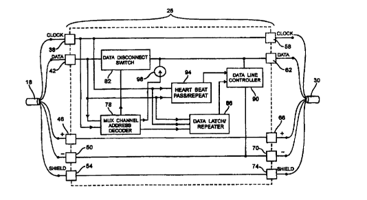
Figure 3 is a block diagram illustrating the main
sections of the multiplex extender 26 and their
interconnections. Each multiplex extender 26 includes a
clock line input terminal 38, a data line input terminal
42, a positive power input terminal 46, a negative power
input terminal 50 and an optional shield input terminal
54 for connecting to the bus line 18 of the time division
multiplexed control bus 10, and a clock line output
terminal 58, a data line output terminal 62, a positive
power output terminal 66, a negative power output 70 and
an optional shield output terminal 74 for connecting to
the branch line 30 and its discrete I/O devices 34. The
clock line, positive power, negative power and shield
input terminals 38, 46, 50 and 54, respectively, are
directly connected to their corresponding clock line,
positive power, negative power and shield output
terminals, 58, 66, 70 and 74, respectively, such that the
clock pulses and power can be passed directly through the
multiplex extender 26 to the branch line 30 and its
discrete I/O devices 34. The input and output terminals
can be either individual terminals or multi-pin
connectors. Inside the multiplex extender 26 are a
multiplex channel address decoder 78, a data disconnect
switch 82, a data latch/repeater 86, a branch line
6
CA 02286598 1999-10-15
WO 99/4!860 PCT/US99/03537
controller 90, and a heartbeat pass-through/repeater 94,
which is optional depending on the control bus system.
The multiplex channel address decoder 78 is user
programmable to any one of the multiplex channel
addresses available on the time division multiplexed
control bus 10. In its simplest form, the multiplex
channel address decoder 78 uses shift registers and
simple logic functions to compare the multiplex channel
address code of each data frame with the settings of a
l0 number of dip switches selectively positioned to indicate
the programmed multiplex channel address code. In more
sophisticated applications a microprocessor in the
multiplex channel address decoder 78 will evaluate the
multiplex channel address of each data frame and compare
it with the multiplex channel address code previously
programmed into an EEPROM or similar device. A multiplex
channel address decoder 98 is described in Riley
5,555,267. The multiplex channel address decoder 78 has
inputs from the clock line input terminal 38 and the data
line input terminal 42 and outputs which connect to the
data disconnect switch 82 and data latch/repeater 86.
The output signals from the multiplex channel address
decoder 78 to the data disconnect switch 82 and data
latch/repeater 86 will either indicate that the
programmed multiplex channel address has been decoded
TRUE or that any of the other multiplex channel addresses
have been decoded FALSE. The multiplex channel address
decoder 78 also has a third output which provides a
current signal 98 to the data line output terminal 62
3o This current signal 98 is provided only in conjunction
with a FAL8E output signal from the multiplex channel
address decoder 78. The current signal 98 charges the
data line of the branch line 30 to a particular level
equivalent to an idle state level of the time division
multiplexed control bus i0 when no data is being
transmitted. In the preferred embodiment, the idle state
of both the time division multiplexed control bus 10 and
the branch line 30 is a HIGH state. However, in other
CA 02286598 1999-10-15
WO 99/41860 PCT/US99/03537
embodiments the idle state of the control bus data line
and the branch line data line could be indicated by
either a HIGH or a LOW state. The current signal 98, in
combination with the branch line controller 90, form a
data driver or data transmitter which transmits selected
data to the branch line 30 when the data disconnect
switch 82 is in an open state. The branch line
controller 90 actively pulls the data line of the branch
line 30 to the opposite of its normal HIGH or LOW idle
state for periods of time determined by inputs to the
branch line controller 90, thereby causing data to be
transmitted to the branch line 30. Other known data
drivers could be used to perform the same function. The
data disconnect switch 82 also has an input from the data
line input terminal 42 and an output which is connected
to a data line output terminal 62. The open or closed
state of the data disconnect switch 82 is controlled by
the input from the multiplex channel address decoder 7s.
The data latch/repeater 86 also has inputs from the clock
line input terminal 38 and the data line input terminal
42 and an output connected to the branch line controller
90, which, in this embodiment, is a normally open control
switch i18 (Fig. 5) electrically connected between the
data output terminal 62 and the negative power line. The
control switch 118 of the branch line controller 90 is
selectively closed and opened electrically by the output
signal from the data latch/repeater 86. The latching
(storing) or repeating of data by the data latch/repeater
86 is controlled by the input from the multiplex channel
address decoder 78. The heartbeat pass-through/repeater
94, when required, has inputs from the clock line input
terminal 38 and the data line input terminal 42 and an
output connected to the branch line controller 90. When
a "heartbeat" pulse is required by the discrete I/O
3s devices 34, the pulse will be passed or repeated by the
heartbeat pass-through/repeater 94. The heartbeat pass-
through/repeater 94 can also use the branch line
controller 90 to pass or repeat the heartbeat pulse.
8
CA 02286598 1999-10-15
WO 99141860 PCT/US99/03537
During normal operation, the multiplex channel
address decoder 78 of each multiplex extender 26 will
read and decode the multiplex channel address located at
the beginning of each data frame to determine if the
multiplex channel address being polled by the bus
controller 14 is its programmed multiplex channel
address. When the multiplex channel address decoder 78
determines that the multiplex channel address being
polled is its programmed address, it will send a signal
to the data disconnect switch 82 causing that switch to
close and thereby permit the data in that data frame to
be passed directly from the data input terminal 42 to the
data output terminal 62 and ultimately to the discrete
I/O devices 34 connected on the branch line 30 of that
particular multiplex extender 26. At the same time, the
multiplex channel address decoder 78 sends a signal to
the data latch/repeater 84 causing it to latch or store
the data of the particular data frame in a volatile
memory means, such as RAM, for future use. The discrete
I/O devices 34 will each read the data addressed to them
in the particular data frame and respond accordingly.
The responses of each discrete I/O device 34 will be sent
back up the branch line 30 to the data output terminal
62, through the closed data disconnect switch 82 to the
data input terminal 42, and then to the bus controller 14
or other addressed I/O devices on the control bus 10.
When the multiplex channel address decoder 78 determines
that the multiplex channel address being polled by the
bus controller 14 is not its programmed address, it will
send a signal to the data disconnect switch 82 causing
the switch to open and thereby prohibit data in that data
frame from being passed to the data output terminal 62.
Simultaneously, the multiplex channel address decoder ~8
will send a current signal 98 of a particular value from
its third output to the data output terminal 62, thereby
actively pulling the data line of its associated branch
line 30 HIGiB for as long as the data disconnect switch 82
is open. The multiplex channel address decoder 78 will
9
CA 02286598 1999-10-15
WO 99/41860 PCT/US99/03537
also send a signal to the data latch/repeater 86 causing
it to repeat the data previously stored during the last
data frame addressed to the programmed multiplex channel
address of that particular multiplex extender 26. The
data latch/repeater 86 repeats its previously stored data
by accessing the branch line controller 90. The output
signals from the data latch/repeater 86 cause the control
switch 118 of the branch line controller 90 to close and
open, which in turn causes the branch line 30 to be
to pulled LOW for a period equal to the time the control
switch 118 is closed. Any responses from the discrete
I/O devices 34 to the repeated data from the data
latch/repeater 86 will not be passed through the open
data disconnect switch 82 to the control bus 10. The
t5 multiplex extender 26 will continue to block all incoming
data frames and repeat the previously stored data until
the next data frame addressed to its programmed multiplex
channel address is received from the network controller
14 and decoded by the multiplex channel address decoder
20 78. At that time, the data disconnect switch 82 will
again be closed, allowing the new data to pass through to
the discrete I/O devices 34 and the data latch/repeater
84 will replace the previously stored data with the new
data being received.
25 In some control buses 10 a "heartbeat" pulse is sent
during each data frame as a data line test. Each I/O
device, 22 or 34, must receive that "heartbeat" pulse or
revert to a predetermined state, usually "OFF". In these
applications the heartbeat pass-through/repeater 94 will
30 receive the heartbeat pulse from the data line input
terminal 42 during each data frame, regardless of the
multiplex channel address, and pass only the heartbeat
pulse to the branch line controller 90, which in turn
passes the heartbeat pulse to the data output terminal 62
35 such that it can be received by the discrete I/O devices
34.
Figure 4 illustrates one embodiment of the data
disconnect switch 82 which is a simple bi-directional
CA 02286598 1999-10-15
WO 99/41860 PCT/US99/03537
analog switch. In this embodiment the data disconnect
switch 82 includes a first FET 102 electrically connected
in series with a second FET 106 such that the sources of
the two FETs, 102 and 106, are connected together and the
drain of the first FET 102 is connected to the data input
terminal 42 while the drain of the second FET i06 is
connected to the data output terminal 62. The gates of
the two FETs 102 and i06 are electrically connected
together such that a signal from the multiplex channel
address decoder 78 controls both FET 102 and FET i06.
When the multiplex channel address decoder 78 decodes its
programmed multiplex channel address in a data frame, it
sends a signal which gates the FETs i02 and 106 "ON".
This permits data received at the data line input
terminal 42~to pass through FETs 102 and 106 to the data
output terminal 62, down the branch line 30 to the
discrete I/O devices 34. In a similar manner, data
returning from the discrete I/0 devices 34 up the branch
line 30 to the data output terminal 62 will pass through
FETs 102 and 106 to the data input terminal 42 and then
to the bus controller Z4 or other I/O devices on the
control bus I0 to which it could be addressed. This bi-
directional passage of data will continue as long as the
FETs 102 and 106 are gated "ON" by the multiplex channel
address decoder 78. When the multiplex channel address
decoder 78 decodes a multiplex channel address other than
its programmed multiplex channel address in a data frame,
it sends a signal gating the FETs i02 and i06 "OFF".
This prevents data from passing in either direction
through the data disconnect switch 82.
Figure 5 illustrates one embodiment of the heartbeat
pass-through/repeater 94 and the branch line controller
90. In this embodiment a first D-latch 1i0 and a second
D-latch ii4 are used to pass through or repeat the
heartbeat pulse from each data frame to the discrete I/O
devices 34, regardless of the multiplex channel address
of the data frame. Inputs to the first D-latch li0
include V+ voltage at the D input, an inverted input from
11
CA 02286598 1999-10-15
WO 99/41860 PCT/US99/03537
the data input terminal 42 at the clock terminal and an
inverted input from the clock input terminal 38 at the
clear terminal. The inputs for the second D-latch 114
include the Q output from the first D-latch 110 at the D
input terminal, an input from the data input terminal 42
at the clock terminal, and an inverted input from the
clock input terminal 38 at the clear input terminal. The
Q output of the second D-latch iid provides the pass-
through or repeat of the heartbeat pulse and is connected
to to the branch line controller 90. In this embodiment,
the control switch 118 of the branch line controller 90
is a FET with its source connected to the negative power
line and its drain connected to the data output terminal
62. The gate of the FET 118 receives the control signal
from the Q output of the second D-latch 114. As the FET
118 is gated "ON", the branch line 3o is pulled LOW, thus
passing through the heartbeat pulse. The branch line
controller 90 works in the same manner when controlled by
an output signal from the data latch/repeater 86 to
2o repeat a latched data frame.
Figure 6 illustrates an example timing graph of the
input and output wave forms from the heartbeat pass-
through/repeater 94. The heartbeat pulse is normally
sent during a synchronization period at the beginning of
each data frame. In this particular example, the sync
period starts at to when the bus controller 14 pulls the
clock signal HIGH and holds it HIGH for 8.5 cycles(t8,5).
At the beginning of the sync period (tp)~ the bus
controller i4 also pulls the data line HIGH for one clock
cycle and then at tl pulls it LOW for two clock cycles
before releasing it to go HIGH for the remainder of the
sync period at t3. When the up-line data line goes LOW
,at the end of the first clock cycle, t~ of the sync
period, the Q output (Ql) of the first D-latch il0 goes
HIGH. After two more clock cycles (t3) the up-line data
line goes HIGB again and the Q output (Q2) of the second
D-latch 114 also goes HIGH. At the end of the sync
period (tg,5) the clock line is driven LOtt and thereby
12
CA 02286598 1999-10-15
WO 99/41860 PCT/US99/03537
resets the Q outputs (Ql and Q2)of both D-latches 110 and
114 to LOW again. The D input (Dl) of the first D-latch
110 is V+ and will remain HIGH throughout the sync
period. The D input (D2) of the second D-latch 114 is
the same as the Q output (Ql) of the first D-latch 110.
The Q output (QZ) of the second D-latch 114 is sent to
the branch line controller 90. The actual heartbeat
pulse passed to the data output terminal 62 by the branch
line controller 90 is the opposite of the Q output (Q2)
of the second D-latch 114. The areas of the timing graph
shown as diagonal lines indicate periods in which the
data line can be either HIGH or LOW.
13