Note: Descriptions are shown in the official language in which they were submitted.
CA 02287036 1999-10-21
DIELECTRIC LINE CONVERTER, DIELECTRIC LINE UNIT,
DIRECTIONAL COUPLER, HIGH-FREQUENCY CIRCUIT MODULE,
AND TRANSMITTER-RECEIVER
BACKGROUND OF THE INVENTION
1. Field of the Invention
The present invention relates to a line converter
between dielectric lines of different kinds, and a
directional coupler, dielectric line unit, high-frequency
circuit module, and transmitter-receiver which use the line
converter.
2. Description of the Related Art
In a circuit using dielectric lines, when lines of, for
example, a waveguide, and so on, which are different in kind,
are used in the input-output portion of the circuit or a
part of the circuit, a line converter between the waveguide
and dielectric line is required. For example, a line
converter between a line made up of a waveguide in which a
dielectric material is loaded(filled) (hereinafter, called
DWG) and a non-radiative dielectric line in which a
dielectric stripline is arranged between parallel conductor
surfaces (hereinafter, called NRD guide) is shown in
Japanese Unexamined Patent Publication No. 8-70209. In this
line converter, the width of the dielectric stripline and
the space of the wall surfaces (between the conductor
CA 02287036 2002-03-27
... ~> _
surfaces) of the w:is~ith directian are gradually widened
over from the DWG t~c> the NRD guide.
In the line coruverter between the above DWG ancL NRD
guide, although thr-,.~ ~.ine converter has an advantage of
low line conversion .oss over a r>road-band, there wa.s a
problem that the line converter becomes large-sized as a
whole because the L:i.rze lengt7. of the line conversion
portion is lengthecik:rd.
For example, as a circuit using dielectric lines, a
directional coupler of a paral:le~.-'wire line type in which
two dielectric str:i~_xlines are :arranged in parallel
between two upper a:~r~d lower ~~ondt~ctor surfaces is used.
An NRD guide can be used as a dielectric line, but the
frequency bandwidth in which the characteristic values of
power distribution erratic, and ao on, are kept within.
fixed values is na:r_~row. When a directional coupler of a
waveguide type is ~:camposed of a DW~,~, a:lthough broad-band
characteristics can be obtained, a line converter between
the above DWG and eJI:::I7 guide is res~uired with a
directional coupler of the DWG in order to realize the
NRD guide as an in.La~..at:-output . ?~s t::he result , the whole
system becomes lar~:~f_~- si~aed.
SUMMARY OF THE INVIls~TION
It is an obje;::t of an aspect. of the present
invention to presecit_ a die:Lectric line converter which is
able to keep a goo;a ~..ine conversion characteristic and is
made small-sized a::> a whole .
Further, it i::~ another ob j ect of an aspect of the
CA 02287036 2002-03-27
present invention t~c:> present a directional coupler having
wide-band characte:u:i.s tics and made up of small-sized.
dielectric lines.
It is further G:moth.er obj ~~ct: of an aspect of th.e
present invention l~c_~ present a hi.~~h-frequency circuit
module and transmil;t~er-receiver using <~ dielectric line
unit or directiona',~ coupler of the above dielectric line
converter.
In an aspect :o the prese;zt invention, a line
converter comprise:: a first-ki,ld dielectric line having
upper and lower su:r_:~aces as a ~orlductor surface of a.
dielectric stripliru=-° and spacers beside the dielectric
stripline, a secon~:a--kind die.Le~~tric line having upper and
lower surfaces and :~~i.de surfac~=s as a conductor surface
of a dielectric st:r~i.pline, and a dielectric striplin.e
connected to the d:~.t~lectri.c striplines of the first-kind
and second-kind dic-~:a.ectric: line or being continuous with
the dielectric str:~~>~-roes of tze first-kind and second-
kind dielectric licm~, wherein ;:.hey space between the upper
and lower conducto:u surfaces i~z the region except th.e
dielectric st:ripli:cic=:~ i.s made narrower than the space
between the upper :~r.~~d lower ;:onductor surfaces in th.e
first-kind line, aa:n~! wherein t:lze .space between the
conductor surfaces :i.n the second-:kind dielectric line
portion is made ne~~:vly zero.
Because of th~~o construction, as the space between
the upper and lower conductor aurfaces sandwiching the
dielectric st:riplicm does not ~ha:nge abruptly over from
the first-kind die ~f_~ctr:ic :Line tc> the second-kind
CA 02287036 2002-03-27
dielectric line (d:irlectri: -loaded waveguide~ , a line
conversion takes place without deteriorating reflection
characteristics, atz~~l as the line does not tend to be
widened in its widf~Ju direction it: becomes easy to make
the line converter small-sized in its width direction.
In the above c~c~>nstruction, when the further they
position is displaced from the first-kind dielectric line
to the second-kind dielectric line, the narrower the
space between the c~c.anductor surfaces except the region of
the dielectric line, the reflection at the discontinuity
portion is further ,~auppressed.
Further, when t:tne .line length between the first.-kind
dielectric line and the second-kind dielectric line is
made an odd mult.ip.lae of a fourth of a wavelength on the
line, the reflected waves at the two locations in which
the space between the upper and lower conductor surfaces
sandwiching the di~s:l.e~ctx~ic: stripline changes are
superposed in opposite phase, anc~ consequently the
reflected waves ar~:~ c:ancelad. Accordingly, the reflection
characteristic is :improved.
Further, in an aspect of the present invention, a
line converter com;p:r-xse~~ a f first-kind dielectric line
having upper and lower surfaces as a conductor surface of
a dielectric
CA 02287036 1999-10-21
- 5 -
stripline and spaces beside the dielectric stripline, a
second-kind dielectric line having upper and lower surfaces
and side surfaces as a conductor surface of a dielectric
stripline, and a dielectric stripline connected to the
dielectric striplines of the first-kind and second-kind
dielectric line or being continuous with the dielectric
striplines of the first-kind and second-kind dielectric line,
wherein the space from the dielectric stripline to the side
conductor surface is made a fixed value which is narrower
than the space from the dielectric stripline of the first-
kind dielectric line to the side conductor surface.
Because of this construction, as the space between the
upper and lower conductor surfaces sandwiching the
dielectric stripline changes in a stepped way over from the
first-kind dielectric line to the second-kind dielectric
line (dielectric-loaded waveguide), the dimension of the
line converter does not have to be long in its length
direction. As the result, a short line converter in its
length direction can be obtained.
In the above construction, when the line length between
the first-kind dielectric line and the second-kind
dielectric line is made an odd multiple of a fourth of a
wavelength on the line, the reflected waves at the two
locations in which the space between the upper and lower
conductor surfaces sandwiching the dielectric stripline
CA 02287036 2002-03-27
_6__
changes are superposed in opposite phase, and consequently
the reflected waves ax-a canceled. F~crordingly, the
reflection characteri~~>t:ic i:a improved.
When the line i,:~ c:omposed of a dielectric line
propagating a single )~.~SM mode (hereinafter, called hyper-
NRD guide) by making i~:he space between the conductor
surfaces of the abovr..a .first-W find dielectric line narrower
than the height of tl:n_a dielectric :atri.pline of the first-
kind dielectric line,. a dielectric line circuit having a
dielectric line and. ca:i.E:lectx: ic-loaded waveguide which
hardly causes any lo;~:_> accompanying a mode conversion at a
bend can be easily coy.°istructed.
Further, in an ,:~:_>pect of the present invention, the
above dielectric line' converter :constitutes a dielectric
line unit. For examp:lE_~, by giving t: he above dielectric' line
converter to a secon;a-kind die:le~tric line, a dielectric
line unit using the sfac;ond-kind dielectric line can be~
constructed so 'that ~:~ f first-~:~ind dielectric line can be
directly connected t,:~ t:he dielectric line unit.
Further, in an aspect of the present invention, tree
above dielectric: line:' c.onv~erter .constitutes a directional
coupler. For example, t:he two se~~orud-kind dielectric lines
which are joined togei:.her or. int~rgrated constitute a
directional coupler. z:n th.i:~ way, a directional coupler
into which input can l:>e given ~hrot~gh an NRD guide and.
which has a broad-ba~;m:f character:ist:ic can be obtained.
Further, in the ;p:I:'f'ser.~t invention, the above dielectric
line unit or directir.~r~al coupler to be used in the
propagation portion o:~: a transmission signal or reception
signal constitutes a ~iigh-frequenc~r circuit module .
CA 02287036 2002-03-27
Furthermore, in the present invention, the above high-
frequency circuit module, and a transmission circuit and
reception circuit r.on::~titute a transmitter-receiver.
In accordance with another aspect of the present
invention, there is provided a die:~ectric line converter
comprising:
upper and lower conduci~or surfaces; and
a dielectric stripline disposed between a portion of
said upper and lower conductor suraaces along a length
thereof ,
wherein a distance between said upper and lower
conductor surfaces varies along a :length of a remainder
thereof such that said upper and lower conductor surfaces
are spaced apart in a :First part of said remainder and the
distance between said conductor surfaces is almost zero in
a second part o.f sai.d remainder .
In accordance with another aspect of the present
invention, there is o~~ovided a die=Lectric line converter
comprising:
a first portion having spaced apart first upper and
lower conductor surfaces, a first dielectric stripline
disposed between said :E_irst upper <~nd lower conductor
surfaces and a space between a remainder of said first
upper and lower conductor surfaces; and
a second portion having second upper and lower
conductor surfaces, at: least cne of said second upper and
lower conductor surfaces having a groove therein, and a
second dielectric stripline disposed in said groove, said
second portion coupled to said first porti.an and said first
dielectric stripline coupled to said second dielectric
CA 02287036 2002-03-27
stripline,
wherein a distance between said second upper and lower
conductor surfaces in a z:emainder c>f said second portion is
almost zero.
In accordance wivh another as~ecu of the present
invention, there is provided a c.iei.ecwric line converl~er
comprising:
a first portion. raving spaced apart first upper and
lower conductor surf:a~~es, a firwt dielectric stripline
disposed between said first upper ~~~.nd lower conductor
surfaces and a pair of spaces, each space on either side of
said dielectric stri.p:line between ~~. remainder of said first
upper and lower concl.u.~~tar surfaces; and
a second portic,n having sec°onct upper and lower
conductor surfaces and side ccnC~uct.or surfaces, at least
one of said second u.p,per and iov,.~er conductor surfaces
having a groove there in, and. a :v~ecc>nd dielectric stripline
disposed in said grr~owe, said secoz~~d portion coupled 1:o
said first portion d.nd said fir~:~t dielectric stripling
coupled to said secc.~n~~ dielectric ~-st:ripline,
wherein a distance between said side conductor
surfaces and said second dielect:ru~: s~ripline is smal:Ler
than the width of e~~.c:h of the spaces in the first port=ion.
BRIEF DESCRIPTION Of''THE DRAWINGS
Figs . lA and LE are perspecti,u~e view: showing the
construction of: a di.el.ect~ric line c;onverte~r according to a
first embodiment of the present invention;
Figs. 2A and 2B are sectional views of each portion of
the dielectric line converter;
CA 02287036 2002-03-27
_c~_
Figs. 3A and 3B are perspective views showing the
construction of a die:lectri~: lire r.:~on~rerter according to a
second embodiment;
Figs. 4A and 4B r~r_e .perspecti're views showing the
construction of a dielectric lire ~:.~onverter according to a
third embodiment;
Figs. 5A, 5B and !iC show sect_Lonal views of each
portion of the diele~ci~:ric line con,~~erter;
Fig. 6 shows the relationship of the characteristic
impedance of the lire to the space between the conduct: or
surfaces;
Fig. 7 shows the reflection characteristic in a fixed
frequency band;
Fig. 8 is a pers.~~ective view showing the construction
of a dielectric line c.:onverter acc~d~x~ding to a fourth
embodiment;
Figs. 9A, 9B and 63C :show sectional views of each
portion of the dieleci~rio. line con,,~~erter of Figure 8;
Fig. 10 shows the relationship of the characteri~~tic
impedance of the lire to the d~~.tan.ce to t:he side conductor
surface away from the die:~ect:r~c s~ripline;
Fig. 11 shows t'Hne reflection characteristic in a fixed
frequency band;
Fig. 12 is a perspective view showing an example of
the construction of a dirE~ctional coupler according to a
fifth embodiment;
Fig. 13 is a top view of the directional coupler with
the upper conductor plate removed;
Fig. 14 shows thc~ distribution characteristic of the
directional coupler;
CA 02287036 2002-03-27
._ya_
Fig. 15 shows a.n example of th.e construction of a
directional coupler a.~cording to a sixth embodiment;
Figs. 16A, 16B and 16C are sec::tional views of each
portion of the direc:~t.iona.l coupler;
Fig. 17 shows thf~ construction. of a directional
coupler used in actual measuretne~nt;
Fig. 18 shows di:~tribution ~haracteristics obtained
through simulation;
Fig. 19 shows di:~tribut.i.on characteristics obtained by
actual measurement;
Fig. 20 shows thf_= construction. of a millimeter wave
radar module according to a sevE:~nte embadiment;
Fig. 21 is a block diagram of the millimeter wave
radar module;
Fig. 22 shows the construction. of a millimeter wave
radar module according to an. eicThta~i embodiment;
Fig. 23 is a block diagram of the millimeter wave
radar module;
Fig. 24 is a bloc~:k diagram of a. transmitter-rece:Lver
according to a nintin. ~cnbc~dimer~t ;
Fig. 25 is an exploded vied- ita. perspective showing an
example of the const:ructian of ~4 di.electric line unit
according to a tents, embc.~dimerbt ;
Fig. 26A is a perspective vie~n~ and Figs. 26B and 26C
are sectional views showing the construction of a
dielectric line converter accordin~c~ to an eleventh
embodiment; and
Figs. 27A and 27B are perspective views showing t:he
construction of a di.rectianal cc:~upl_er according to a
CA 02287036 2002-03-27
_9b_
twelfth embodiment.
DESCRIPTION OF THE F:REFERRED EMBODIMENT
CA 02287036 1999-10-21
- 10 -
The construction of a dielectric line converter
according to a first embodiment of the present invention is
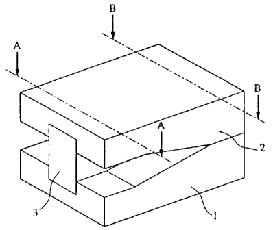
shown in Figs. 1 and 2. Fig. 1A is a perspective view of
the whole of the main part, and Fig. 1B is a perspective
view of Fig. 1A in which the upper conductor plate is
removed. And Fig. 2A is a sectional view taken on line A -
A of Fig. 1A, and Fig. 1B is a sectional view taken on line
B - B.
In Fig. 1, reference numerals 1 and 2 represent a
conductor plate which is composed of an electrode film
formed on the surface of a molded insulating plate or a
conductor plate which is composed of a processed metal plate,
respectively. Reference numeral 3 represents a dielectric
stripline produced by injection molding or cutting work,
which is made up of synthetic resin, ceramics, or their
composite materials. As shown in the figure, by arranging
the dielectric stripline 3 between the upper and lower
conductor plates 1 and 2, a first-kind dielectric line, a
second-kind dielectric line, and a line conversion portion
therebetween are constructed.
The dimension in height and width direction of the
dielectric stripline 3 is constant in any one of the first-
kind dielectric line, second-kind dielectric line, and line
conversion portion. As shown in Fig. 2, in the first-kind
dielectric line portion, the space h between the opposing
CA 02287036 1999-10-21
- 11 -
surfaces (conductor surfaces) of the upper and lower
conductor plates is made to be smaller than the height
dimension of the dielectric stripline 3. In this way, a
hyper-NRD guide (indicated by HNRD in the figure)
propagating a single LSMO1 mode is constructed. In the
second-kind dielectric line portion, the upper and lower
conductor plates 1 and 2 are put one on another, that is,
the space between the opposing surfaces is made to be nearly
zero. Accordingly, the groove depth in the conductor plates
of the second-kind dielectric line portion is set to be half
of the height dimension of the dielectric stripline 3. In
this way, the second-kind dielectric line is made a
dielectric-loaded waveguide (indicated by DWG in the figure).
In the line conversion portion (indicated by TR in the
figure), the groove depth is gradually changed so that the
space between the opposing surfaces of the upper and lower
conductor pates 1 and 2 becomes tapered over from the first-
kind dielectric line portion to the second-kind dielectric
line portion. Because of this construction, the reflection
is reduced at the input-output portions or half-way, and a
good reflection characteristic is maintained as a line
converter.
Fig. 3 shows the construction of a dielectric line
converter according to a second embodiment. Different from
the first embodiment, in the example shown in Fig. 3, the
CA 02287036 1999-10-21
- 12 -
space between the opposing surfaces of the upper and lower
conductor plates 1 and 2 of the line conversion portion is
changed stepwise from the space in the first-kind dielectric
line portion to the space (nearly zero) in the second-kind
dielectric line portion. In such a construction also, as
the space difference in the portion in which the space
between the opposing surfaces of the upper and lower
conductor plates 1 and 2 changes stepwise is small, the
reflection is suppressed to be low, and the total reflection
characteristic can be kept good.
Next, the construction of a dielectric line converter
according to a third embodiment is explained with reference
to Figs. 4 through 7.
Fig. 4A is a perspective view of the whole of the main
part, and Fig. 4B is a perspective view of Fig. 4A in which
the upper conductor plate is removed. Reference numerals 1
and 2 represent a conductor plate, and reference numeral 3
represents a dielectric stripline. This dielectric
stripline is made up of synthetic resin, ceramics, or their
composite materials, and PTFE of dielectric constant er =
2.04 is used in the examples showing characteristics to be
described later.
A sectional view of each portion is shown in Fig. 5.
Fig. 5A is a sectional view in the first-kind dielectric
line portion, Fig. 5B is a sectional view in the line
CA 02287036 1999-10-21
- 13 -
conversion portion, and Fig. 5C is a sectional view in the
second-kind dielectric line portion. The height and width
of the dielectric stripline 3 are 2.2 mm and 1.8 mm,
respectively, and are constant in any of the first-kind
dielectric line, second-kind dielectric line, and line
conversion portion. The groove depth given in the conductor
plate of the first-kind dielectric line portion is made 0.5
mm, the groove depth in the line conversion portion is 0.65
mm, and the groove depth in the second-kind dielectric line
is 1.1 mm.
Here, the relationship of the characteristic impedance
of the line to the space between the conductor surfaces of
the upper and lower conductor plates 1 and 2 is shown in Fig.
6. Z1 represents the characteristic impedance of the first-
kind dielectric line, and Z2 represents the characteristic
impedance of the second-kind dielectric line. When the
space between the conductor surfaces is determined so that
the characteristic impedance of the line conversion portion
is given by (ZI~Z2), the impedance matching between the
lines of the two kinds can be realized. In this example,
the space between the conductor surfaces is 0.9 mm. And
when the wavelength on the line is assumed to be ~,g, the
line length L of the line conversion portion is set to be
~.g/4 or an odd multiple of T,g/4. In the example, the
wavelength is in a 60 GHz band and L is 1.85 mm.
CA 02287036 1999-10-21
- 14 -
Fig. 7 shows the reflection characteristic of a
dielectric line converter constructed as in the above which
is based on the three-dimensional finite element method. In
this way, a low reflection characteristic of -30 dB can be
obtained in a 60 GHz band.
Next, the construction of a dielectric line converter
according to a fourth embodiment is explained with reference
to Figs. 8 through 11.
Fig. 8 is a perspective view of a dielectric line
converter with the upper conductor plate removed. In this
example, the space between the upper and lower conductor
plates of a first-kind dielectric line portion is kept
constant, and the space between the upper and lower
conductor plates of a second-kind dielectric line is made
nearly zero. However, in a line conversion portion, the
groove is expanded toward the side of a dielectric stripline
3, and the groove depth in that portion is made the same as
the groove depth of the conductor plate in the first-kind
dielectric line.
A sectional view of each portion of the above
dielectric line converter is shown in Fig. 9. Fig. 9A is a
sectional view of the first-kind dielectric line portion,
Fig. 9B is a sectional view of the line conversion portion,
and Fig. 9C is a sectional view of the second-kind
dielectric line portion. The height and width of the
CA 02287036 1999-10-21
- 15 -
dielectric line 3 are 2.2 mm and 1.8 mm, respectively, and
are constant in any of the first-kind dielectric line,
second-kind dielectric line, and line conversion portion.
The groove depth given in the conductor plate of the first-
kind dielectric line portion is made 0.5 mm. The groove
depth in the line conversion portion is also 0.5 mm, but the
space to the side conductor surface in the line conversion
portion is made 0.16. The groove depth in the second-kind
dielectric line is 1.1 mm.
Here, the relationship of the characteristic impedance
of the line to the distance from the dielectric stripline to
the side conductor surface is shown in Fig. 10. Z1
represents the characteristic impedance of the first-kind
dielectric line, and Z2 represents the characteristic
impedance of the second-kind dielectric line. When the
space from the dielectric stripline to the side conductor
surface is determined so that the characteristic impedance
of the line conversion portion is given by (Zl~Z2), the
impedance matching between the lines of the two kinds can be
realized. In this example, the space is 0.16 mm. And when
the wavelength on the line is assumed to be ~,g, the line
length L of the line conversion portion is set to be ~.g/4 or
an odd multiple of ~,g/4. In the example, the wavelength is
in a 60 GHz band and L is 1.83 mm.
Fig. 11 shows the reflection characteristic of a
CA 02287036 1999-10-21
- 16 -
dielectric line converter constructed as in the above which
is based on the three-dimensional finite element method. In
this way, a low reflection characteristic of -30 dB can be
obtained in a 60 GHz band.
Next, an example of the construction of a directional
coupler according to a fifth embodiment is explained with
reference to Figs. 12 through 14.
Fig. 12 is a perspective view of a directional coupler
with the upper conductor plate removed, and Fig. 13 is its
top view. The portions indicated by 31, 32, 33, and 34 are
dielectric striplines, and in the example they are
integrally molded substantially in a H-shape. In the
conductor plate 1 grooves in which the dielectric stripline
31 through 34 are fitted to a certain depth are formed. The
upper conductor plate also has the same construction.
As constructed this way, over from the dielectric
stripline 32 to dielectric stripline 34, the line conversion
takes place in order of the first-kind dielectric line, line
conversion portion, second-kind dielectric line, line
conversion portion, and first-kind dielectric line. In like
manner, over from the dielectric stripline 31 to 33, the
line conversion takes place in order of the first-kind
dielectric line, line conversion portion, second-kind
dielectric line, line conversion portion, and first-kind
dielectric line.
CA 02287036 1999-10-21
- 17 -
The above dielectric striplines are integrated in a
part of the portion constituting the second-kind dielectric
line. Because of this, the second-kind dielectric line
portion is made to function as a directional coupler of DWG.
The directional coupler of DWG shows a broad-band
characteristic just as the directional coupler using a
cavity waveguide is broad-band. Furthermore, as the four
parts can be used as hyper-NRDs, when a directional coupler
is given in a dielectric line circuit using a hyper-NRD
guide, the whole of them can be made greatly small-sized.
In the above directional coupler, the space between the
upper and lower conductor plates of the first-kind and
second-kind dielectric line portion and the space between
the upper and lower conductor plates of the line conversion
portion are the same as in the example shown as the third
embodiment in Fig. 5. And the dimension and material of the
dielectric striplines are the same as in the third
embodiment. The dimension of each portion shown in Fig. 13
is the values of a directional coupler designed for a 60 GHz
band, and they are expressed in a unit of mm.
Fig. 14 shows the distribution characteristic based on
the three-dimensional finite element method. Thus, in the
60 GHz band as a designed band S31 and S41 characteristics
are within -3 dB to result in an equal distribution
characteristic, and, furthermore, the characteristic is
CA 02287036 1999-10-21
- 18 -
maintained over a broad band.
Next, an example of a directional coupler according to
a sixth embodiment is explained with reference to Figs. 15
through 19.
Fig. 15 is a top view of a directional coupler with the
upper conductor plate removed. The directional coupler is
basically the same as what is shown in Fig. 13, but the
directional coupler to be used in a 76 GHz band is shown
here. As the directional coupler is used in the higher
frequency band, the line length of the TR conversion portion
is made 1.3 mm and in the second-kind dielectric line
portion the dimension of the portion to couple the parallel-
wire lines is made smaller than shown in Fig. 13.
Fig. 16 shows the sectional view of the line portions
of the three kinds in the above directional coupler. Fig.
16A is a sectional view of the first-kind dielectric line
portion, Fig. 16B is a sectional view of the line conversion
portion, and Fig. 16C is a sectional view of the second-kind
dielectric line portion. As the directional coupler is used
in the higher frequency band, the dimension of each portion
is made smaller than shown in Fig. 5.
Fig. 17 shows the constriction of a directional coupler
the characteristics of which were practically investigated,
and is a top view of only the dielectric stripline portion.
In this directional coupler, the power of the input signal
CA 02287036 1999-10-21
- 19 -
from port No. 1 is distributed to No. 2 and No. 3. Because
a hyper-NRD guide is entirely constituted outside the
conversion portion TR, even if a bend of an arbitrary
curvature is constructed, any loss accompanying mode
conversion does scarcely occur. In the example, a bend
having a radius of curvature of 5 mm (R5) is formed in order
to lead out port No. 4 in a direction at a right angle to a
straight line connecting port No.l and port No. 3.
Fig. 18 shows the result of the directional coupler
shown in Fig. 15 which was simulated as no loss system using
the three-dimensional finite element method. Fig. 19 is the
result of an actual measurement of the directional coupler
shown in Fig. 17. It is able to make the power distribution
ratio nearly constant over such a broad frequency band.
Next, based on Figs. 20 and 21, an example of the
construction of a millimeter wave radar module according to
a seventh embodiment is explained. Fig. 20 is a top view of
the module with the upper conductor plate removed, and Fig.
21 a block diagram of the above millimeter wave radar module.
The millimeter wave radar module is principally made up
of each unit of oscillator, isolator, directional coupler,
circulator, and mixer. In the oscillator, a millimeter wave
signal is generated by a Gunn diode. The isolator is made
up of a terminator connected to one port of the circulator
which port three dielectric striplines as shown in the
CA 02287036 1999-10-21
- 20 -
figure. That is, in the isolator, the millimeter wave
signal from the oscillator is made propagated to the side of
the directional coupler, and it is arranged that the
reflected signal from the directional coupler is lead to the
terminator. The directional coupler is of the same
construction as that shown in Fig. 12, and is given the four
ports of a hyper-NRD guide to distribute an input signal
from port No. 1 to port No. 3 and port No. 4 in a fixed
power distribution ratio. The signal from port No. 3 is
radiated as a TX signal toward a target from an antenna
connected to an RF port through the circulator. The
reflected signal from the target which the antenna received
is input as an RX signal to the mixer through the circulator.
On the other hand, a signal from port No. 4 of the
directional coupler is input to the mixer as an LO signal,
and the mixer mixes the RF signal and LO signal. When the
signal from the oscillator has two-valued frequencies fl and
f2 over the course of time, an IF signal having a frequency
component of fl - f2 in accordance with the time difference
caused by the path difference between two paths can be
obtained. By processing this IF signal, the distance to the
target is measured.
Next, the construction of a millimeter wave radar
module according to an eighth embodiment is shown in Fig. 22
and 23. Fig. 22 is a top view with the upper conductor
CA 02287036 1999-10-21
- 21 -
plate removed, and Fig. 23 is a block diagram of the above
millimeter wave radar module.
The millimeter wave radar module is principally made up
of each unit of oscillator, isolator, directional coupler,
circulator, up-converter, and down converter. In the
oscillator, a millimeter wave signal is generated by a Gunn
diode. The isolator is made up of a terminator connected to
one port of the circulator which port three dielectric
striplines as shown in the figure, and in the isolator the
millimeter wave signal from the oscillator is made
propagated to the side of the directional coupler and it is
arranged that the reflected signal from the directional
coupler is lead to the terminator. The signal input from
port No. 1 of the directional coupler is output from port No.
3 and port No. 4, respectively, and input to the up-
converter and the down converter. The up-converter mixes an
LO signal from the directional coupler and an IF signal from
an IF circuit, and outputs a signal containing a frequency
signal of LO and IF to the circulator. This signal is
radiated outside as a TX signal through the circulator. In
this example, the signal is output to a waveguide through a
WG converter to convert a hyper-NRD guide to a waveguide
mode. The signal reflected from a target is input as an RX
signal into the down converter through the circulator. The
down converter mixes the LO signal oscillated in the
CA 02287036 1999-10-21
- 22 -
oscillator and the RX signal and an IF signal containing an
RX - LO component is obtained. By processing the frequency
change of the IF signal given to the above up-converter and
the frequency component of the IF signal obtained from the
down converter, the distance to the target is measured.
Fig. 24 is a block diagram showing the construction of
the whole of a transmitter-receiver according to a ninth
embodiment, in which the above millimeter wave radar module
is used. In Fig. 24, the RF circuit corresponds to the
above millimeter wave radar module, and the IF circuit is
made up of a filter circuit and AD converter for the IF
signal obtained from the millimeter wave radar module. The
signal processing circuit measures the distance from the
antenna of the millimeter wave radar module to the target
and calculates the relative speed by signal-processing or
computing the digital data of the IF signal, and when
required external circuits of mobile engine control units,
and so on, are controlled.
Next, the construction of a dielectric line unit
according to a tenth embodiment is shown in Fig. 25. In Fig.
25, reference numerals 1 and 2 represent upper and lower
conductor plates, and 3a and 3b represent divided upper and
lower dielectric striplines. Further, 4 represents a board
in which a microstrip line 5, and so on, are formed, and the
board sandwiched between the upper and lower conductor
CA 02287036 1999-10-21
- 23 -
plates 1 and 2 constitutes a dielectric line unit. This
dielectric line unit corresponds to a unit having the
construction shown in Fig. 4 which is divided up and down at
the middle portion and sandwiches the board therebetween.
By the microstrip line 5 inserted in a DWG portion in a
direction at a right angle to the line of the DWG, a line
conversion between the DWG and microstrip line is performed.
And generation of unwanted waves is reduced by such a line
conversion between the DWG and microstrip line, compared
with the case in which a direct line conversion between an
NRD guide and microstrip line is carried out. More, a
hollow portion is formed in the portion of the conductor
plate 2 which is opposed to the microstrip line 5 so that
the microstrip line 5 is not made in direct contact with the
upper conductor plate 2.
More, in each of the embodiments shown in the above, an
example in which a line conversion between a hyper-NRD guide
and dielectric-loaded waveguide is performed was shown.
However, when a line conversion between a normal NRD guide
and dielectric-loaded waveguide in which both modes of a
LSMO1 mode and LSE01 mode are propagated is carried out, the
present invention can be equally applied. The example is
shown in Fig. 26.
In Fig. 26A is a perspective view of the whole of the
main part, Fig. 26B is a sectional view taken on line B - B
CA 02287036 1999-10-21
- 24 -
of Fig. 26A, and Fig. 26C is a sectional view taken on line
C - C of Fig. 26A. Different from the construction shown in
Fig. 1, no groove is given in the upper and lower conductor
plates 1 and 2 of the normal NRD guide in this example.
In the line conversion portion (TR), the groove depth
is gradually changed so that the space between the opposing
surfaces of the upper and lower conductor plates 1 and 2
becomes tapered over from the normal NRD guide portion to
the DWG portion.
Further, in each of the embodiments shown in the above,
the conductor surface of a dielectric line was made up of
the surface of a conductor plate. However, the conductor
surface may be formed by metallizing a fixed portion of a
dielectric stripline. Regarding a directional coupler, the
example is shown in Fig. 27.
Fig. 27A is a perspective view of a dielectric
stripline, and Fig. 27B is a perspective view of the
directional coupler with the upper conductor plate removed.
The portions indicated by 31, 32, 33, and 34 are dielectric
lines, but different from the example shown in Fig. 12 an
electrode film is formed on a dielectric stxipline portion
constituting the DWG. The construction of the others is the
same as in Fig. 12.
Because of this construction, in the DWG portion the
metallized electrode functions as a conductor surface, and
CA 02287036 1999-10-21
- 25 -
accordingly even if a more or less spacing is caused between
the dielectric stripline and the conductor plate in the DWG
portion a stable characteristic can be always realized.
According to a first aspect of the present invention,
because the discontinuity portion over from a first-kind
dielectric line to a second-kind dielectric line is lessened,
a line conversion is made without deterioration of
reflection characteristics. Furthermore, as the line does
not tend to be widened in its width direction, a dielectric
line converter which is small-sized in its width direction
can be obtained.
According to a second aspect of the present invention,
the reflection at the discontinuity portion of the line over
from a first-kind dielectric line to a second-kind
dielectric line is more suppressed.
According to a third and fifth aspect of the present
invention, reflected waves at two discontinuity portions are
superposed in opposite phase, and as a result the reflected
waves are canceled. Because of this the reflection
characteristic is improved.
According to a fourth aspect of the present invention,
because the space between the upper and lower conductor
surfaces sandwiching a dielectric stripline is changed
stepwise over from a first-kind dielectric line to a second-
kind dielectric line, the dimension in length direction of a
CA 02287036 1999-10-21
- 26 -
line converter which is short suffices. Therefore, a line
converter which is short in its length direction can be
obtained.
According to a sixth aspect of the present invention, a
dielectric line circuit having an NRD guide and DWG which
practically do not cause any loss accompanying the mode
conversion in a bend can be easily constructed.
According to a seventh aspect of .the present invention,
when, for example, an element of a DWG is given to a
dielectric line circuit, the element becomes possible to be
directly connected in a dielectric line circuit of an NRD
guide, and as a result it becomes possible to make the whole
of small size.
According to an eighth aspect of the present invention,
because input and output can be done at NRD guides and a
directional coupler of a DWG can be constructed, a
directional coupler having broad-band characteristics and of
small size can be realized.
According to a ninth aspect of the present invention, a
small-sized high-frequency circuit module having broad-band
characteristics in which the directional coupler or
dielectric line unit is used in the propagation portion of a
transmission signal or reception signal can be easily
constructed.
According to a tenth aspect of the present invention, a
CA 02287036 1999-10-21
- 27 -
small-sized transmitter-receiver having broad-band
characteristics in which the high-frequency circuit module,
transmission circuit, and reception circuit are given can be
constructed.
While the invention has been particularly shown and
described with reference to preferred embodiments, it will
be understood by those skilled in the art that the foregoing
and other changes in form and details can be made without
departing from the spirit and scope of the invention.