Note: Descriptions are shown in the official language in which they were submitted.
CA 02287441 1999-10-19
WO 99/43096 PCT/US98/27003
DATA COMMUNICATIONS TERMINAL AND METHOD
OF ADJUSTING A POWER SIGNAL GENERATED THEREFROM
Field of the Invention
The invention relates generally to a data communication system and
in particular to a data communication terminal and method for
automatically adjusting a power level in response to a detected change in
the data communications terminal.
Background of the Invention
Data communication systems are well known and include a terminal
device that communicates with a portable data device in either a
contacted or contactless mode. Delivering power from the terminal
device to the portable data device in a contacted arrangement is rather
easily controlled through the electrical connections of the contact points.
In a contactiess environment, power delivery and regulation can be a more
complex problem. In particular, it is imperative that the portable data
device receives enough energy to maintain a suitable power level for the
card circuitry, but not too much power so that the device circuitry begins
to overheat.
To help explain the dynamics of a card receiving too much power,
FIG. 1-1 shows a data communication system 100 that includes a terminal
device 102 in relation to a portable data device 104. As shown, the
transmitting element 106 of the terminal device 102 is separated from
the receiving element 108 of portable data device 104 by a distance, D. It
is well understood that the amount of energy seen by the portable data
CA 02287441 1999-10-19
WO 99/43096 2 PCT/US98/27003
device 104 is directly related to the distance, D, between the card and the
reader. That is, as the card comes closer to the reader, the card must
adapt to the increased energy by somehow regulating the power to
maintain a constant level.
FIG. 1-2 shows a graphical depiction of the relationship between the
distance, D, and the card power, P~. The power curve 110 shows an
exponentially decreasing relationship between the card power and the
distance between the card and the reader. To maintain proper operating
conditions, there is a minimum distance 112 that the card can be
separated from the reader. At this distance, the card sees the maximum
power that can be tolerated by the circuitry on the card. When the card
moves closer to the reader, the excess power must be absorbed by any
number of known means, such as resistive elements, etc. When the card
and reader are separated by a distance shown in region 116, the card must
continually absorb the excess power so that the card circuitry is not
damaged. Of course, power absorbed in resistive elements generates heat,
which can build up and cause deleterious effects on the card substrate
(usually some form of plastic). Likewise, as the card moves away from
the reader, as depicted in region 118, the power seen by the card
decreases to a minimal acceptable level 120 at a maximum allowable
distance 122.
While the problem of minimum power levels are being addressed by
advanced reception techniques, the problem associated with maximum
power levels that result in card over-heating remain persistent in today's
smart cards. Prior art techniques that address this problem require that
the card remain in communication with the terminal, allowing for a
feedback mechanism to request that the terminal deliver less power. The
need for communication from the card to the reader becomes a problem
when, for one reason or another, the card ceases communicating with the
3 0 reader. One such scenario is when the card loses synchronization with the
CA 02287441 1999-10-19
WO 99/43096 3 PCT/US98/27003
reader, whereby the feedback mechanism is lost. Another scenario is
when the card and reader do not communicate in the same format. In
either case, the card is unable to convey to the reader the presence of
excess power, and overheating results. In fact, a card IC could get so hot
that it could distort the plastic and cause thermal damage to
semiconductor junctions, thereby rendering the card useless.
Accordingly, there exists a need for a data communication system
terminal and method for adjusting a power level for delivery to a portable
data device. In particular, a data terminal that could automatically adjust
the power level without requiring communications between the card and
reader (e.g., a request from the card to adjust the power level) would be
an improvement over the prior art.
Brief Description of the Drawings
FIG. 1-1 shows a data communication system, as is known in the art;
FIG. 1-2 shows a power curve that relates detected power levels
with distance between the terminal and portable data devices shown in
FIG. 1-1;
FIG. 2 shows more detailed diagram of a terminal device, in
accordance with the present invention;
FIG. 3 shows a simplified schematic diagram of a power delivery
mechanism, in accordance with one embodiment of the present invention;
FIG. 4 shows a simplified schematic diagram showing several
impedance detection techniques, in accordance with the present invention;
FIG. 5 shows a simplified schematic diagram depicting a power
regulation circuit, in accordance with the invention; and
F1G. 6 shows a data flow diagram depicting operation of a terminal
device, in accordance with the present invention.
CA 02287441 1999-10-19
WO 99/43096 4 PCT/US98/27003
Detailed Description of a Preferred Embodiment
The present invention encompasses an apparatus and method for use
in a data communications terminal that includes an antenna for delivering
a power signal to a portable data device. The data communications
terminal monitors an impedance characteristic for the antenna,
attempting to detect a change in the monitored impedance characteristic
thereof. When a change is detected, the data communications terminal
automatically adjusts a power level of the power signal delivered to the
portable data device. In this manner, the present invention allows for a
communication-less means by which the power delivered to the card can
be adjusted by the terminal (i.e., without the need for the reader
requesting a power adjustment).
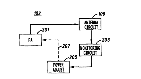
FIG. 2 shows a simplified block diagram of a data communications
terminal 102, in accordance with the present invention. A power
amplifier 201 generates and delivers a power signal to the antenna circuit
106, for transmission to the portable data device. During operation, the
antenna circuit 106 delivers impedance characteristic information to a
monitoring circuit 203, which can be implemented in a number of
different ways, as later described. The monitoring circuit 203 is operably
coupled to a power adjustment circuit 205, in accordance with the
present invention. Finally, the power adjust circuit 205 generates a
control signal 207 that is inputted to the power amplifier 201. According
to the present invention, the foregoing simplified elements are used to
advantageously provide power adjustment without an attendant need to
receive a command from the portable data device. Accordingly, it is not
necessary that the card and the reader be in communication for a power
adjustment to be made
CA 02287441 1999-10-19
WO 99/43096 5 PCT/US98/27003
FIG. 3 shows a balanced transmitter circuit that can be used in the
power amplifier 201 shown in FIG. 2. The power amplifiers 201-1 and
201-2 are driven by opposite-polarity input signals 302 and 304, such
that the voltage swing across the antenna circuit 106 is double what it
would be with only a single-ended, unbalanced drive circuit. In a
preferred embodiment, the inductor 306 needs to be resonated, at the
power amplifier carrier frequency, using resonating capacitors 308, 310
such that the maximum current is obtained through the antenna for a given
drive voltage (i.e., out of the power amplifiers). Maintaining a completely
balanced circuit for the antenna has the added benefit of controlling
radiated emissions, as fewer spurious radiating modes are excited with
an antenna that is balanced with respect to ground.
FIG. 4 shows the antenna circuit 106 shown in FIG. 3, along with a
plurality of monitoring circuits, in accordance with the present invention.
In particular, between nodes 401 and 402 is shown a first monitoring
circuit 403. In one embodiment, the current through the inductor 306 is
sampled using a series connected primary coil 405 of a transformer
circuit, that is completed with the secondary coil 407. The carrier
current flowing through the inductor 306 typically has a large amplitude,
on the order of 0.5 amps to greater than 1 amp, in order to generate
sufficient magnetic field to power a remotely coupled card. By making
the turns ratio of the secondary coil 407 to the primary coil 405 high, the
sampled current is stepped down to a value appropriate for a high
impedance detector circuit 409. In this embodiment, the high impedance
detector circuit 409 produces a control signal 410 that is proportional to
the current flowing through the antenna circuit 106. Of course, a large
turns-ratio lowers the impedance of the detector that is reflected into
the primary circuit between nodes 401 and 402, thereby negligibly
affecting the series losses in the antenna circuit 106.
CA 02287441 1999-10-19
WO 99/43096 6 PCT/US98/27003
The voltage across the inductor 306 (i.e., between the two nodes 411
and 402) can also be sampled as a means of monitoring the impedance
characteristic. In one embodiment, the voltage is measured across the
nodes by utilizing the inherent subtraction operation of a simple high-
s impedance differential amplifier 413 to produce a control signal 414. In
practice, the voltage swing between nodes 411 and 402 can be very large
for a high current system, on the order of 50 Vpeak, so some resistive
divider or other means of reducing the voltage across the differential
amplifier input nodes may be required (not shown). The voltage across the
antenna can produce an impedance characteristic in and of itself, or when
used in conjunction with the antenna series-current sense performed by
403 (or 416, as next described), an actual antenna impedance can be
calculated from the sensed antenna voltage and current. It should be
noted that the differential voltage measurement between nodes 411 and
402 does not generally provide an accurate measure of the antenna
current. This is because the actual impedance seen between nodes 402
and 411 is dependent on the proximity of the card to the reader. However,
in spite of it's inherent inaccuracy, this voltage measurement is
sufficient to generate a control signal for use in a power control method,
in accordance with the invention.
A second embodiment for sampling the series current through the
inductor 306 (and third technique for monitoring an impedance
characteristic) uses a monitoring circuit 416, in which a known series
impedance 417 is placed between nodes 411 and 415. This impedance
does not have to be resistive; a reactance or complex impedance is also
useful, provided the impedance is known. By measuring the voltage drop
across nodes 415- 411 with a high-impedance differential amplifier 419,
a control signal 420 is generated that is proportional to the antenna
series current.
CA 02287441 1999-10-19
WO 99/43096 7 PCT/US98/27003
A preferred embodiment for the power amplifier system is shown in
FIG. 5, wherein amplifier 501 may be any high-efficiency, saturated-mode
amplifier. In a preferred embodiment, a class D amplifier is used. There
are several ways the amplifier's output power level can be controlled, in
accordance with the present invention. First, by applying the control
signal (CS', CS", etc.) to an amplifier power supply circuit 502, which
consists of a DC-DC converter 504 and a supply filter 506, the bias to the
power amplifier can be adjusted. Adjusting the bias of a saturated-mode
power amplifier as a means of adjusting the output power is well
understood by those skilled in the art. Another means of adjusting the
power in the fundamental frequency coming out of the amplifier is to
alter the drive signal to the amplifier with a modulating circuit 508 that
will vary the duty cycle of the input drive waveform using a pulse-width
modulator. The maximum carrier level can be achieved for a 50% duty
cycle. For a pulse width modulated drive waveform having a duty cycle b,
those skilled in the art can show that the fundamental component of the
pulse waveform varies as sin(n8)/r~. This function has a maximum for
b=0.5, or 50% duty cycle, and falls off symmetrically whether the duty
cycle is increased or decreased.
In one embodiment, the voltage sampled across a series impedance
is compared to the power amplifier supply voltage. As the presence of the
card de-tunes the resonance, the current through the antenna starts
decreasing since the card's additional impedance is coupled into the
antenna. As the ratio of the sampled current to the power amplifier
supply voltage (which serves as an operating impedance characteristic)
starts decreasing, the ratio can be monitored. When the monitored ratio
falls below a predetermined threshold or outside of a predetermined
range, which indicates the proximity of the card, the supply bias can be
reduced by a predetermined amount, in accordance with the invention. As
CA 02287441 1999-10-19
WO 99/43096 g PCT/US98/27003
the card recedes from the reader, the ratio again increases, and the power
amplifier supply is returned to its initial level.
In some applications, it is preferred to have the antenna remotely
located from the power amplifier 501. in such a case, the power signal is
directed to the antenna through a standard transmission line, such as a
50 or other standard impedance coaxial cable. To efficiently deliver
power to the antenna, it must be impedance-matched to the cable
impedance using a matching network 520. Changes in the antenna
impedance may be observed at the power amplifier end of the cable by
utilizing the impedance characteristic monitoring circuit 512. This
circuit consists of a bi- directional coupler 516 which in general consists
of coupled transmission lines but for low frequencies such as used in the
preferred embodiment, would consist of lumped inductors and capacitors.
Such circuits are well known in the art. By comparing the forward and
reverse-propagating waves, the reflection coefficient 518 (denoted by 'T")
can be calculated, which those skilled in the art recognize as another
means of representing impedance at the input to the matching network.
Through de-imbedding techniques, the effects of the matching network
520 can be removed to yield the actual antenna impedance, if desired.
However, knowing the value of r is all that is necessary to observe the
change in antenna impedance sufficiently well to engage power control.
For a power amplifier that is intended to drive a 50-ohm cable,
another means of controlling the output power (i.e., besides power supply
control) is to utilize variable attenuator 514, which is driven by a control
signal derived from the reflection coefficient 518. For example, in one
embodiment, observing the reflected waveform amplitude, which is
indicative of the antenna de-tuning due to the proximity of a card, and
comparing it to the incident amplitude, a feedback control signal can be
generated to control the attenuator or amplifier power supply. It should
be noted that, for 50-ohm systems having the antenna located near the
CA 02287441 1999-10-19
WO 99/43096 9 PCT/US98/27003
power amplifier, this measurement can be made without the directional
coupler by observing the voltage amplitude at the input to the matching
network, since the voltage at this point is the sum of the incident and
reflected waves. Comparing this amplitude to the "no-card-present"
amplitude, which serves as a reference impedance characteristic, the
incident wave amplitude can be reduced to keep the incident-plus-
reflected amplitude constant. Of course, this approach reduces the power
delivered to the card in close proximity, and increases the incident wave
to "no-card-present" levels as the card recedes from the reader.
FIG. 6 shows a flow diagram 600 that depicts operation of a data
communications terminal in accordance with the present invention.
During operation, the terminal monitors (601 ) its own impedance
characteristic for the antenna circuit, as earlier described. A function of
the antenna impedance, f(ZA), is calculated (603) using one or a
combination of two of the techniques earlier described. When the
calculated impedance is compared with a reference impedance
characteristic, which might be a voltage or digital word that corresponds
to a preferred operating condition, and determined (605) to be within
range, the impedance characteristic is continually monitored (at step
601 ). In the event that the calculated impedance characteristic falls
outside of a predetermined range, the power signal is adjusted (607) by a
predetermined amount by the data communications terminal. In
particular, if the power signal is either too low or too high, as determined
by a corresponding impedance change in the terminal, the power signal is
adjusted accordingly. It is important to note that the terminal is able to
make an automatic power adjustment based on monitoring its own
characteristics. Thus, a card that has lost communication or cannot
initiate communication with the reader stands to benefit equally as one
that maintains continuous communication with the reader.
CA 02287441 1999-10-19
WO 99/43096 1 O PCT/US98/27003
The above features describe a communication-less power control
system, where, by means of relatively low-complexity circuits, a reader
terminal can gather sufficient information about the proximity of a card
to effect a transmit power reduction as a card nears a reader. Likewise,
transmit power can be automatically increases as a card separates from a
previously reduced-power reader. The advantage of not requiring
communications lies in the fact that the card may be unable to
communicate with the reader because of a difference in communications
format or some other non-communicating mode, such as the card being in
the field with another card that is controlling the communications link, or
an error in the communications link causing lost synchronization. With
more and more financial and other sensitive applications relying on the
use of contactless smart cards, the amount of information that can be
destroyed by overheating a card is increasing dramatically. Accordingly, a
terminal and method for adjusting the power levels transmitted
therefrom toward a contactless card provide a significant improvement
over the prior art.
What is claimed is: