Note: Descriptions are shown in the official language in which they were submitted.
CA 02288807 2003-03-27
1
D E S C R I P T I O N
FINGERPRINT READING APPARATUS
Technical Field
The present invention relates to a reading
apparatus for reading a target object having a fine
recessed or projecting pattern such as a fingerprint.
Background Art
A conventional reading apparatus for reading a
target object having a fine recessed or projecting
pattern such as a fingertip has a structure like the
one disclosed in USP No. 5,635,723 in which a
two-dimensional photosensor is formed on a surface
light source, and an optical component is formed on the
two-dimensional photosensor. The invention of this
reference detects changes in capacitance when a finger
touches the optical component, and sequentially detects
the detection results as electric charges, which are
generated by photosensors arranged two-dimensionally
and correspond to an incident light quantity from the
optical component. In this structure, many light guide
fibers are mounted on the two-dimensional photosensor
without any optical lens, so that the whole apparatus
can be downsized. Recently, another type of structure
is examined in which an optical component formed from
many light guide fibers is made thinner into a light
CA 02288807 2003-03-27
2
scattering film or in which the upper surface of a photosensor is covered with
a
transparent resin layer having an uneven surface without any optical
component. For example, this type of structure is disclosed in U.S. Patent No.
6, 310, 683.
In this reading apparatus, a finger directly touches the upper surface of
the two-dimensional photosensor. If the finger is charged with static
electricity,
this static electricity may cause a malfunction of the two-dimensional
photosensor or may damage it in the worst case. If the pattern of a
fingerprint is
copied onto a sheet by any means, since the reading apparatus is not equipped
with any means for discriminating a sheet from a human finger, the apparatus
determines matching so long as the pattern is the same. When this fingerprint
matching is set as a log-in condition for a personal computer or a host
computer of a network, the computer cannot be reliably protected from a third
person's access.
Disclosure of Invention
It is the first object of the present invention to provide a reading
apparatus which prevents a photosensor from malfunction or damage by
static electricity. It is the second object of the present invention to
provide a
reading apparatus capable of ensuring the reliability by reading a pattern
after,
CA 02288807 1999-11-02
WO 99/46724 PCT/JP99101189
3
e.g., detecting whether the object is man.
According to the present invention, there is
provided a reading apparatus for reading a target
object having a shadow pattern, comprising a light
source, a photosensor device having a plurality of
photosensors formed on the light source, and a
transparent conductive layer formed on the photosensor
device.
According to the present invention, there is
provided a reading apparatus for reading a target
object having a shadow pattern, comprising: a light
source; a photosensor device having a plurality of
photosensors formed on the light source; at least one
pair of transparent conductive layers formed on the
photosensor device to detect a resistance of a target
object; and an operator for, when a value of the
resistance of the target object, which is detected
falls within the predetermined value, starting reading
the target object.
Additional objects and advantages of the invention
will be set forth in the description which follows, and
in part will be obvious from the description, or may be
learned by practice of the invention. The objects and
advantages of the invention may be realized and
obtained by means of the instrumentalities and
combinations particularly pointed out hereinafter.
CA 02288807 1999-11-02
WO 99/46724 PCT/JP99101189
4
Brief Description of Drawings
The accompanying drawings, which are incorporated
in and constitute a part of the specification,
illustrate presently preferred embodiments of the
invention, and together with the general description
given above and the detailed description of the
preferred embodiments given below, serve to explain the
principles of the invention.
FIG. 1 is an enlarged sectional view of part of a
fingerprint reading apparatus according to the first
embodiment of the present invention;
FIG. 2 is a plan view of part of the fingerprint
reading apparatus shown in FIG. 1;
FIG. 3 is a block diagram of the fingerprint
i5 reading apparatus shown in FIG. 1;
FIG. 4 is a circuit diagram of a photosensor
section and photosensor driver shown in FIG. 3;
FIG. 5 is an equivalent circuit diagram of a
single photosensor shown in FIG. 1;
2fl FIGS. 6A to 6D are circuit diagrams for explaining
changes in voltage applied to each electrode of the
photosensor shown in FIG. 5 and state of the photo-
sensor;
FIG. 7 is a plan view of part of a fingerprint
25 reading apparatus according to the second embodiment of
the present invention;
FIG. 8 is a circuit diagram of part of the
CA 02288807 2003-03-27
fingerprint reading apparatus shown in FIG. 7;
FIG. 9 is a plan view of part of a fingerprint reading apparatus according
to the third embodiment of the present invention;
5 FIG. 10 is a circuit diagram of part of the fingerprint reading apparatus
shown in FIG. 9; and
FlG. 11 is a plan view showing a modification of the fingerprint reading
apparatus shown in FIG. 9.
Best Mode of Carrying Out the Invention
(First Embodiment)
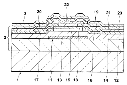
FIG. 1 is a sectional view of part of a reading apparatus according to
the first embodiment of the present invention. This reading apparatus can read
a target object in any form having a fine recessed or projecting pattern. In
the
following embodiment, the reading apparatus will exemplify a fingerprint
reading apparatus for reading a fingerprint. This fingerprint reading
apparatus
has a two-dimensional photosensor (photosensor device) 2 on a surface light
source 1. A transparent conductive layer 3 made of ITO (Indium Tin Oxide)
or the like is formed on the two-dimensional photosensor 2. The surface
light source 1 is formed of an electroluminescence or formed as an edge
light type backlight used in a liquid crystal display device. Although
not shown, the edge light type backlight typically has a light-reflecting
plate on the lower surface of a light guide plate, one or several point
CA 02288807 1999-11-02
WO 99/46724 PCT/JP99/01189
6
light sources such as light-emitting diodes are
disposed next to the light guide plate, and a surface
of the point light source that does not correspond to
the light guide plate is covered with a light-
s reflecting sheet. The transparent conductive layer 3
dissipates static electricity and is grounded in a
given region {not shown). The transparent conductive
layer 3 is formed by, e.g., deposition on the upper
surface of an overcoat film 23 {to be described later)
of the two-dimensional photosensor 2. The transparent
conductive layer 3 is formed slightly larger than a
square sensor region 4 of the two-dimensional
photosensor 2 indicated by the one-dot chain line in
FIG. 2. Note that the two-dot chain line in FIG. 2
represents a finger 5.
The two-dimensional photosensor 2 will be
described. The two-dimensional photosensor 2 has a
structure in which a plurality of photosensors 11 (only
one photosensor is shown in FIG. 1) are arranged in a
matrix. The two-dimensional photosensor 2 has a
transparent substrate 12 made of an acrylic resin,
glass or the like. A bottom gate electrode 13 serving
as a light-shielding electrode made of chromium or
aluminum is formed for each photosensor 11 on the upper
surface of the transparent substrate 12. A light-
transmitting bottom gate insulating film 14 made of
silicon nitride is formed on the entire upper surface
CA 02288807 1999-11-02
WO 99/46724 PCT/JP99/01189
7
of the bottom gate electrode 13 and the upper surface
of the transparent substrate 12. A semiconductor layer
15 made of amorphous silicon is formed on an upper
surface portion of the bottom gate insulating film 14
which corresponds to the bottom gate electrode 13.
n+-type silicon layers 16 and 17 are respectively
formed on the two sides of the semiconductor layer 15
on the upper surface of the bottom gate insulating film
14. A light-transmitting blocking layer 18 made of
silicon nitride is formed on the upper surface of the
semiconductor layer 15. Source and drain electrodes 19
and 20 as light-shielding electrodes made of chromium
or aluminum are formed on the two sides of the upper
surface of the blocking layer 18, the upper surfaces of
the n+-type silicon layers 16 and 17, and the upper
surface of the bottom gate insulating film 14. A
light-transmitting top gate insulating film 21 made of
silicon nitride is formed on the entire upper surfaces
of the source and drain electrodes 19 and 20 and the
exposed surface of the blocking layer 18. A top gate
electrode 22 as a transparent electrode made of ITO or
the like is formed on an upper surface portion of the
top gate insulating film 21 which corresponds to the
semiconductor layer 15. A light-transmitting overcoat
film 23 made of silicon nitride is formed on the entire
upper surface of the top gate electrode 22 and the
upper surface of the insulating film 21. In this
CA 02288807 1999-11-02
WO 99/46724 PCT/JP99/01189
8
two-dimensional photosensor 2, when a light beam is
incident at random from the lower surface side, one
part of the light beam is shielded by the bottom gate
electrode 13, and the other part of the light beam
passes through the light-transmitting layers excluding
the source and drain electrodes 19 and 20, so that the
light beam is not directly incident on the semi-
conductor layer 15.
Operation of this fingerprint reading apparatus
will be explained in short. A light beam emitted from
the upper surface of the surface light source 1 passes
through the light-transmitting portion of the
two-dimensional photosensor 2 and the transparent
conductive layer 3. The finger 5 (see FIG. 2) in
contact with the transparent conductive layer 3 is
irradiated with this transmitted light beam at random
from the lower surface side. The light beam reflected
by the surface of the finger 5 passes through the
transparent conductive layer 3 and the neighboring top
gate electrode 22 serving as a transparent electrode,
and is incident on the incident surface (exposed
surface) of the semiconductor layer 15 between the
source and drain electrodes 19 and 20. In this case,
portions corresponding to projections (ridges) of the
skin surface of the finger 5 in contact with the
surface of the transparent conductive layer 3 become
bright. Portions corresponding to recesses (valleys)
CA 02288807 1999-11-02
WO 99/46724 PCT/JP99101189
9
of the skin surface of the finger 5 become dark. As a
result, an image whose contrast is optically emphasized
in accordance with the ridges and valleys of the skin
surface of the finger 5 can be obtained to read the
fingerprint of the finger 5.
In this fingerprint reading apparatus, since the
transparent conductive layer 3 is formed and grounded
on the two-dimensional photosensor 2, static
electricity discharged from the finger 5 in contact
with the transparent conductive layer 3 on the
two-dimensional photosensor 2 can dissipate via the
transparent conductive layer 3. This can prevent the
two-dimensional photosensor 2 from malfunction or
damage by this static electricity.
FIG. 3 is a block diagram showing part of the
fingerprint reading apparatus. This fingerprint
reading apparatus comprises a photosensor section 31, a
photosensor driver 32, a CTR (controller) 33, a clock
generation section 34, an A/D (analog-to-digital)
conversion section 35, an S/P (serial-to-parallel)
conversion section 36, a standard pattern memory 37, a
collation section 38, a determination section 39, and
the like.
As shown in FIG. 4, the photoserisor section 31 has
a structure in which the photosensors 11 constituting
the two-dimensional photosensor shown in FIG. 1 are
arranged in a matrix. As shown in FIG. 1, the
CA 02288807 1999-11-02
WO 99/46724 PCT/JP99/01189
photosensor has a bottom gate type transistor formed by
the bottom gate electrode {BG) 13, semiconductor layer
15, source electrode (S) 19, drain electrode (D) 20,
and the like, and a top gate type transistor formed by
5 the top gate electrode (TG) 22, semiconductor layer 15,
source electrode (S) 19, drain electrode {D) 20, and
the like. That is, the photosensor is constituted by
a photoelectric conversion thin-film transistor in
which the bottom gate electrode (BG) 13 and top gate
10 electrode (TG) 22 are respectively formed below and
above the semiconductor layer 15. The equivalent
circuit of this transistor is shown in FIG. 5.
Referring back to FIG. 4, the bottom gate
electrode (8G) of each photosensor 11 is connected to
one of a plurality of bottom electrode lines 41
extending in the row direction. The drain electrode
(D) of each photosensor 11 is connected to one of a
plurality of signal lines 42 extending in the column
direction. The top gate electrode (TG) of each
photosensor 11 is connected to one of a plurality of
top electrode lines 43 extending in the row direction.
The source electrode (S) of each photosensor 11 is
grounded.
As shown in FIG. 4, the photosensor driver 32
shown in FIG. 3 comprises a bottom address decoder 44
serving as a vertical scanning circuit connected to the
bottom electrode lines 41, a column switch 45 serving
CA 02288807 1999-11-02
WO 99/46724 PCTIJP99/01189
I1
as a horizontal scanning circuit connected to the
signal lines 42, and a top address decoder 46 connected
to the top electrodes 43. The bottom address decoder
44 applies a bottom gate voltage VBG to the bottom gate
electrodes (BG) of the photosensors 11 aligned on each
row via a corresponding bottom electrode line 41. The
top address decoder 46 applies a top gate voltage VTG
to the top gate electrodes (TG) of the photosensors 11
aligned on each row via a corresponding top electrode
line 43.
The column switch 45 receives a drain voltage VDD
via a precharge transistor 47. The column switch 45
outputs an output signal VpUT via a buffer 48. Every
time the precharge transistor 47 is turned on upon
reception of a precharge voltage Vp~, the column switch
45 outputs an output from each photosensor 11 connected
to a signal line 42 as the output signal VpUT via the
buffer 48.
The clock generation section 34 shown in FIG. 3
includes an oscillation circuit and a frequency
division circuit, and outputs clock and reset signals
having predetermined frequencies to the CTR 33. The
CTR 33 outputs the bottom and top gate voltages VBG and
VTG as sense and reset signals to the photosensor
driver 32 on the basis of the clock and reset signals
input from the clock generation section 34, and outputs
the precharge and drain voltages Vp~ and VDD to the
CA 02288807 1999-11-02
WO 99/46724 PCT/JP99/01189
12
precharge transistor 47 shown in FIG. 4.
The A/D conversion section 35 shown in FIG. 3
A/D-converts the output signal Vout output from the
photosensor section 31 via the photosensor driver 32
(i.e., the column switch 45 shown in FIG. 4). The S/P
conversion section 36 converts the serial output
signals from the A/D conversion section 35 into
parallel output signals. Fingerprint image signals
corresponding to fingerprints of a plurality of
specific persons are stored as standard pattern signals
in the standard pattern memory 37 in advance. The
collation section 38 collates an output signal from the
S/P conversion section 36 with standard pattern signals
sequentially read out from the standard pattern memory
37, and outputs each collation signal to the deter-
urination section 39. The determination section 39
determines based on the collation signal from the
collation section 38 whether a fingerprint image signal
corresponding to the output signal VpUT from the
photosensor section 31 matches the standard pattern
signal of a specific person stored in the standard
pattern memory 37 in advance, and outputs a determina-
tion signal.
Operation of the photosensor 11 will be described
with reference to FIGS. 5 and 1. When a positive
voltage (e. g., +10V) is applied to the bottom gate
electrode (BG) while a positive voltage (e.g., +5V) is
CA 02288807 1999-11-02
WO 99/46724 PCT/JP99/01189
13
kept applied between the source electrode (S) and drain
electrode (D) of the photosensor 11, a channel is
formed in the semiconductor layer 15 to flow a drain
current. In this state, when a negative voltage (e. g.,
-20V) having a level enough to make the channel formed
by the electric field of the bottom gate electrode {BG)
disappear is applied to the top gate electrode (TG),
the electric field from the top gate electrode (TG)
acts in a direction to eliminate the channel formed by
the electric field of the bottom gate electrode (GB),
thereby pinching off the channel. At this time, when
the semiconductor layer 15 is irradiated with a light
beam from the top gate electrode (TG) side, the
electron-hole pairs are induced in the semiconductor
layer 15 on the top gate electrode (TG) side. The
electron-hole pairs are accumulated in the channel
region of the semiconductor layer 15 to cancel the
electric field of the top gate electrode (TG). A
channel is then formed in the semiconductor layer 15 to
flow the drain current. This drain current changes in
accordance with a change in incident light amount of
the semiconductor layer 15. As described above, in
this two-dimensional photosensor 2, the electric field
from the top gate electrode (TG) acts in a direction to
prevent channel formation using the electric field of
the bottom gate electrode (8G) to pinch off the channel.
The drain current obtained when no light beam is
CA 02288807 1999-11-02
WO 99/46724 PCT/JP99/01189
I4
incident can be greatly reduced, e.g., to about 10-14 A.
The difference between the drain current obtained when
no light beam is incident and the drain current
obtained when a light beam is incident can be made
sufficiently large. The amplification factor of the
bottom gate type transistor at this time can change in
accordance with a change in incident light amount to
increase the S/N ratio.
In the two-dimensional photosensor 2, one
photosensor 11 can have both a sensor function and a
selection transistor function. These functions will be
briefly described below. When a voltage of, e.g., OV
is applied to the top gate electrode (TG) while a
positive voltage (+lOV) is kept applied to the bottom
gate electrode (BG), holes are discharged from the trap
level between the semiconductor layer 15 and the top
gate insulating film 21 to allow refresh or reset
operation. More specifically, when the reading
apparatus is continuously used, the trap level between
the semiconductor layer 15 and the top gate insulating
film 21 is buried with the holes generated upon
irradiation and the holes injected from the drain
electrode (D). A channel resistance set while no light
beam is incident is reduced, and the drain current
obtained when no light beam is incident increases.
Therefore, the top gate electrode {TG) is set at OV to
discharge these holes to allow reset operation.
CA 02288807 1999-11-02
WO 99146724 PCTIJP99/01189
When the positive voltage is not applied to the
bottom gate electrode (BG), no channel is formed in the
bottom gate type transistor. Even if a light beam is
incident, no drain current flows to set the nonselected
5 state. More specifically, by controlling the voltage
applied to the bottom gate electrode (8G), the selected
state and the nonselected state can be controlled. In
the nonselected state, when OV is applied to the top
gate electrode (TG), the holes can be discharged from
10 the trap level between the semiconductor layer 15 and
the top gate insulating film 21 to allow reset
operation in the same manner as described above.
As a result, as shown in FIGS. GA to 6D, for
example, the top gate voltage VTG is controlled to OV
15 and -20V to allow control of the sensed state and the
reset state. The bottom gate voltage VgG is controlled
to OV and +10V to allow control of the selected state
and the nonselected state. That is, by controlling the
top gate voltage VTG and the bottom gate voltage VgG,
one photosensor 11 can have both the function serving
as a photosensor and the function serving as the
selection transistor.
Operation of the two-dimensional photosensor 2
will be explained with reference to FIGS. 3 and 4. The
clock generation section 34 outputs clock and reset
signals having predetermined frequencies to the CTR 33.
The CTR 33 outputs the bottom and top gate voltages VgG
CA 02288807 1999-11-02
WO 99146724 PCTlJP99/01I89
16
and VTG as sense and reset signals to the photosensor
driver 32 on the basis of the clock and reset signals
from the clock generation section 34, and outputs the
precharge and drain voltages Vp~ and VDp to the
precharge transistor 47.
Photosensors 11 on the first row are reset by
setting the bottom and top gate voltages VgG and VTG to
OV. During this resetting, the precharge voltage Vp~
is applied to the precharge transistor 47 for a
predetermined time, and the drain voltage VDD (+5V) is
applied to all the signal lines 42 to precharge the
photosensors 11. The top gate voltage VTG is set to
-20V to change the photosensors 11 to a sense state.
The bottom gate voltage VgG is set to +10V to change
the photosensors 11 to a selected state. An output
signal VpUT from each photosensor 11 changes to OV or
remains at +5V depending on the incident light quantity
(light quantity). The output signal VpUT from each
photosensor 11 is output from the column switch 45 via
the buffer 48. The same operation is performed for
photosensors 11 on the second to final rows. A
description of the subsequent operation will be omitted.
(Second Embodiment)
FIG. 7 is a plan view showing part of a
fingerprint reading apparatus according to the second
embodiment of the present invention. In this
fingerprint reading apparatus, a pair of transparent
CA 02288807 1999-11-02
WO 99/46724 PCT/JP99/01189
17
conductive films 3A and 3B in a comb tooth shape are
formed within and around a sensor region 4 on the upper
surface of an overcoat film 23 of a two-dimensional
photosensor 2. When a finger 5 touches the two-
s dimensional photosensor 2 including the pair of
transparent conductive films 3A and 3B, the pair of
transparent conductive films 3A and 3B detect the
resistance of the touching finger 5 and start
fingerprint reading operation by this detection signal
(to be described later). The pair of transparent
conductive films 3A and 3B can also have an antistatic
function. The pair of transparent conductive films 3A
and 3B are formed into a comb tooth shape in order to
detect a relatively small resistance of the finger 5
with high sensitivity.
FIG. 8 shows part of the circuit of the
fingerprint reading apparatus. In FIG. 8, the same
reference numerals as in FIG. 4 denote the same parts,
and a description thereof will be properly omitted.
One transparent conductive film 3A is connected via a
resistor 51 to a CTR 33 (see FIG. 3) for outputting
the drain voltage VDD, whereas the other transparent
conductive film 3B is grounded. The CTR 33 is
connected between one transparent conductive film 3A
and the resistor 51 via an inverter 52. The CTR 33
outputs a switching signal to a switch controller 53
upon reception of an H-level signal from the inverter
CA 02288807 1999-11-02
WO 99/46724 PCT/JP99/01189
18
52. The switch controller 53 outputs a switch control
signal to a switch 54 upon reception of the switching
signal from the CTR 33. The switch 54 is a normally
open switch formed between a column switch 45 and a
precharge transistor 47.
In the fingerprint reading apparatus, when the
finger 5 touches the two-dimensional photosensor 2
including the pair of transparent conductive films 3A
and 3B, a resistance corresponding to a touch portion
of the finger 5 is generated between the pair of
transparent conductive films 3A and 3B to decrease the
potential between the transparent conductive film 3A
and the resistor 51 to a potential divided by the
resistor 51 and the resistance value of the finger.
The input of the inverter 52 falls from H level to L
level to change the output of the inverter 52 to H
level, and this H-level signal is output to the CTR 33.
The CTR 33 outputs a switching signal to the switch
controller 53 upon reception of the H-level signal from
the inverter 52. Upon reception of the switching
signal from the CTR 33, the switch controller 53
outputs a switch control signal to the switch 54 to
close the switch 54. Then, the column switch 45 is
connected to the precharge transistor 47 via the switch
54 to set the same state as shown in FIG. 4 and start
fingerprint reading operation.
As described above, in the fingerprint reading
CA 02288807 1999-11-02
WO 99/46724 FCT/JP99/01189
19
apparatus, when the finger 5 touches the two-
dimensional photosensor 2 including the pair of
transparent conductive films 3A and 3B, the resistance
of the touching finger 5 is detected to start
fingerprint reading operation by this detection signal.
Fingerprint reading operation can start automatically,
conveniently. Since the other transparent conductive
film 3B applied to most of the sensor region 4 of the
two-dimensional photosensor 2 is grounded, as shown
in FIG. 7, the antistatic function is enhanced. Note
that when, for example, a copying sheet on which a
fingerprint image of the finger 5 is copied is placed
on the two-dimensional photosensor 2 including the
pair of transparent conductive films 3A and 3B, no
resistance is detected by the pair of transparent
conductive films 3A and 3B because the copying sheet is
insulated, and thus illicit use by the copying sheet
can be prevented.
(Third Embodiment)
FIG. 9 is a plan view of part of a fingerprint
reading apparatus according to the third embodiment of
the present invention. In this fingerprint reading
apparatus, pairs of transparent conductive films 3A and
3B in a comb tooth shape are respectively formed on the
four corners of a square sensor region 4 on the upper
surface of an overcoat film 23 of a two-dimensional
photosensor 2. When a finger 5 touches the
CA 02288807 1999-11-02
WO 99/46724 PCTIJP99/01189
two-dimensional photosensor 2 including the four pairs
of transparent conductive films 3A and 3B, the four
pairs of transparent conductive films 3A and 3B detect
the resistance of the touching finger 5 and start
5 fingerprint reading operation by this detection signal
(to be described later). These pairs of transparent
conductive films 3A and 3B can also have an antistatic
function.
FIG. 10 shows main part of the circuit of the
10 fingerprint reading apparatus. In FIG. 10, the same
reference numerals as in FIG. 8 denote the same parts,
and a description thereof will be properly omitted.
The output sides of four inverters 52 corresponding to
the four pairs of transparent conductive films 3A and
15 3B are connected to both a CTR 33 and the input side of
one AND circuit 55. The output side of the AND circuit
55 is connected to the CTR 33.
In this fingerprint reading apparatus, when the
finger 5 touches the two-dimensional photosensor 2
20 including the four pairs of transparent conductive
films 3A and 3B, resistances corresponding to touch
portions of the finger 5 are generated between the
respective pairs of transparent conductive films 3A and
38, the outputs from the four inverters 52 change from
L-level signals to H-level signals, and these H-level
signals are output to the AND circuit 55. When the AND
circuit 55 receives the H-level signals from all the
CA 02288807 1999-11-02
WO 99146724 PCT1JP99/01189
21
four inverters 52, it outputs an AND signal to the CTR
33. In this case, the inverters 52 directly output the
H-level signals to the CTR 33, but the CTR 33 ignores
these H-level signals. Referring to FIG. 8, the CTR 33
outputs a switching signal to a switch controller 53
upon reception of the AND signal from the AND circuit
55. Upon reception of the switching signal from the
CTR 33, the switch controller 53 outputs a switch
control signal to a switch 54 to close the switch 54.
Then, a column switch 45 is connected to a precharge
transistor 47 via the switch 54 to set the same state
as shown in FIG. 4 and start fingerprint reading
operation.
In this fingerprint reading apparatus, when the
touch position and state (whether the finger 5 touches
appropriately) of the finger 5 with respect to the
sensor region 4 of the two-dimensional photosensor 2 is
erroneous, i.e., the finger 5 does not touch all the
four pairs of transparent conductive films 3A and 3B,
the AND circuit 55 outputs no AND signal. In this case,
the finger 5 touches one to three pairs of transparent
conductive films 3A and 3B out of the four pairs of
transparent conductive films 3A and 3B, and inverters
52 corresponding to the pairs of transparent conductive
films 3A and 3B touched by the finger 5 output H-level
signals to the CTR 33. The CTR 33 outputs a finger
touch error signal to a controller (not shown) on the
CA 02288807 1999-11-02
WO 99146724 PCT/JP99/01189
22
basis of the absence of the AND signal from the AND
circuit 55 and the presence of the H-level signals from
the inverters 52. The controller informs the operator
of the erroneous touch position or state of the finger
5 with respect to the sensor region 4 of the two-
dimensional photosensor 2 by any informing means such
as a display "please place your finger again" or voice.
(Modification of Third Embodiment)
This fingerprint reading apparatus can exhibit an
antistatic function because the other transparent
conductive film 3B of each pair is grounded as shown in
FIG. 10. In the third embodiment, however, the central
portion in the sensor region 4 is less resistant to
static electricity because the pairs of transparent
conductive films 3A and 3B are respectively formed at
the four corners of the square sensor region 4 on the
two-dimensional photosensor 2, as shown in FIG. 9.
Therefore, for example, an electrostatic dissipation
transparent conductive film 3C in an almost cross shape
may be formed at the central portion in the sensor
region 4, as shown in FIG. 11.
Note that in the fingerprint reading apparatus in
FIG. 1, the transparent substrate 12 is placed on the
surface light source 1, and the photosensor section 31
having photoelectric conversion thin-film transistors
is formed on the transparent substrate 12. Alter-
natively, the transparent substrate 12 may be omitted,
CA 02288807 1999-11-02
WO 99/46724 PCT/JP99/01189
23
and the photosensor section 31 having photoelectric
conversion thin-film transistors may be directly formed
on a light guide plate constituting the surface light
source 1. Each photosensor is not limited to the
double gate type photoelectric conversion thin-film
transistor described in the above embodiments, and may
be a single gate type thin-film transistor or diode
type thin-film transistor.
As has been described above, according to the
present invention, since the transparent conductive
layer formed on the photosensor device has an
electrostatic dissipation function, even if, e.g., a
finger in contact with the transparent conductive layer
on the photosensor device is charged with static
electricity, this static electricity can dissipate via
the transparent conductive layer. The photosensor
device can be prevented from malfunction or damage by
the static electricity. In addition, a pair of
transparent conductive layers are formed apart from
each other. The resistance value of a target object
placed between the conductive layers is measured to
determine whether the resistance value falls within a
predetermined range. Only when collation is attained,
collation starts. Collation using a copy can be
avoided to improve the reliability.
Additional advantages and modifications will
readily occur to those skilled in the art. Therefore,
CA 02288807 1999-11-02
WO 99/46724 PCT/JP99/01189
24
the invention in its broader aspects is not limited to
the specific details and representative embodiments
shown and described herein. Accordingly, various
modifications may be made without departing from the
spirit or scope of the general inventive concept as
defined by the appended claims and their equivalents.