Note: Descriptions are shown in the official language in which they were submitted.
CA 02288873 1999-11-05
WO 98/51114 PCT/SE98/00750
SHORT PACKET CIRCUIT EMULATION
BACKGROUND
The present invention relates to telecommunication systems in which
asynchronous transfer mode (ATM) is used for transporting voice-type data as
well as
other types of data, for example, video and control data. More particularly,
the present
invention relates to a telecommunication system in which ATM is used for
transporting
low bit rate, circuit emulation data (i.e., synchronous data) from one or more
circuit
to emulation connections (i.e., circuit emulation data sources).
ATM is a standard protocol that is commonly used for transmitting
asynchronous telecommunication data within a telecommunication system for one
or
more applications. ATM is based on the transmission of data in fixed size data
packets
known as ATM cells. The protocol for each ATM cell is the same, wherein, each
ATM cell contains a 48 octet payload and a 5 octet header. In general, ATM is
well
known in the art.
The telecommunication data associated with each application is initially
in a data transfer format that is application specific. If ATM is to be used
for
transporting the data, the application specific data format is adapted so that
it is
2 o compatible with the ATM protocol. This is accomplished by an ATM
adaptation layer
(AAL) 101, as illustrated in FIG. 1. Referring now to FIG. 1, the application
layer
102 represents telecommunication data arriving from a specific
telecommunication data
application. The task of the AAL 101, as mentioned, is to reformat the data so
the data
is compatible with the ATM protocol. Once reformatted, the ATM layer 103 can
2 5 transpart the data to a desired receiving unit.
One of the more common AALs is AAL1. AAL1 is typically used to
packetize synchronous data (i.e., circuit emulation data) into standardized
data packets,
which can, in turn, be structured or unstructured data. Structured data is
organized
into a sequence of data blocks, wherein the boundary for each data block is
defined by
30 a structured data pointer (SDP). The SDP is specifically used for alignment
(i.e.,
CA 02288873 1999-11-OS
WO 98/51114 PCT/SE98/00750
-2-
recovery) of the data at a receiving unit. Unstructured data refers to raw
data that
includes no framing information.
AAL1 is divided into two basic functional sublayers, as illustrated in
FIG. 1: a segmentation and reassembly (SAR) sublayer 104 and a convergence
sublayer
105. The SAR sublayer 104 packetizes the incoming data into data blocks that
are 47
bytes in length. The SAR sublayer 104 then adds a 1 byte sequence number and a
1 bit
data type identifier (to identify the incoming data as either structured or
unstructured).
For example, if the data type identifier bit is set, the first byte in the
block will contain
a SDP. The convergence sublayer supports data packetization, clock recovery,
cell
1 o delay variation compensation and forward error correction.
There are a number of inherent problems associated with AAL1.
Foremost is that the time delay required by AAL1 to prepare a 47 byte data
block is
excessively long. For example, a typical service rate (i.e., the incoming data
rate) for
circuit emulation data is 64 kbits per second. The corresponding time delay
for AAL1
would be approximately 6 milliseconds (i.e., 47 bytes/8 kbytes per second).
Moreover, the transportation of data from a sending unit to a receiving unit
typically
involves several ATM transitions; thus, the already excessive delay is
compounded
with each ATM transition. In addition, when dealing with low bit rate data,
there is
often an insufficient amount of data to completely fill each ATM cell.
Pursuant to the
2o ATM cell protocol, the AAL1 may have to fill the remaining portion of each
ATM cell
with padding bits. This, in turn, results in poor bandwidth utilization. Since
many
applications, such as voice data, are highly sensitive to data transportation
delays, and
because bandwidth is very expensive, there is a real need to design a more
efficient
way to transport low bit rate, circuit emulation data using ATM.
SUMMARY OF INVENTION
Another commonly employed AAL is AAL2, which is sometimes
referred to as AALm. AAL2, is typically used to transform low bit rate,
asynchronous
data, such as cellular voice data. More particularly, AAL2 segments low bit
rate data
3 o streams into small data packets, which are often called minicells or
microcells. The
CA 02288873 1999-11-OS
WO 98/51114 PCT/SE98/00750
-3-
small data packets from a particular low bit rate, asynchronous data source
are then
multiplexed together with small packets from other similar data sources to
form ATM
cells. By segmenting the data into smaller, variable size data packets and by
multiplexing the small packets from multiple data sources, data transportation
delays
are reduced and bandwidth utilization is improved. In addition, transportation
delays
can be further reduced and bandwidth utilization further improved by allowing
the
small data packets to overlap between adjacent ATM cells, as illustrated in
FIG. 2.
The present invention improves the ATM performance for circuit
emulation data using the functional capabilities associated with AAL2. Hence,
the
l0 present invention is essentially an enhanced version of AAL2, and the
present invention
is herein referred to as the circuit emulation adaptation layer. In accordance
with FIG.
3, the present invention is achieved by replacing the AAL 101, illustrated in
FIG. 1,
with a circuit emulation adaptation layer 305 and a short packet multiplexing
layer 310,
wherein the latter is functionally similar or identical to the AAL2 described
above.
Accordingly, it is an object of the present invention to packetize the low
bit rate, circuit emulation data before transporting the data over an ATM
connection.
It is another object of the present invention to improve bandwidth
utilization when transporting circuit emulation data over an ATM connection.
In accordance with one aspect of the invention, the foregoing and other
2 0 objects are achieved by an apparatus, system and/or method for
transporting circuit
emulation data. This involves the transformation of emulation data into a
sequence of
circuit emulation data packets, and then the insertion of the sequence of
circuit
emulation data packets into a data transfer cell. Next, the data transfer cell
is
transported to a receiving unit as a function of a data transfer cell shaping
clock. In
2 5 addition, the length of each data packet is controlled as a function of
the data transfer
cell shaping clock.
In accordance another aspect of the invention, the foregoing and other
objects are achieved by an apparatus, system and/or method for transporting
circuit
emulation data. This involves transforming the circuit emulation data into a
sequence
3 0 of circuit emulation data packets and inserting the sequence of circuit
emulation data
CA 02288873 1999-11-OS
WO 98/51114 PCT/SE98/00750
-4-
packets into a data transfer cell. Then the data transfer cell is transported
to a
receiving unit. Here, data packet length is controlled as a function of the
service rate .
clock.
BRIEF DESCRIPTION OF THE DRAWINGS
The objects and advantages of the invention will be understood by
reading the following detailed description in conjunction with the drawings in
which:
FIG. 1 depicts the asynchronous transfer mode (ATM) adaptation layer
(AAL) in accordance with the prior art;
1 o FIG. 2 illustrates the multiplexing of short packets into ATM cells in
accordance with the prior art;
FIG. 3 depicts an AAL in accordance with the present invention;
FIG. 4 illustrates a short packet including a header and padding
information;
I5 FIGS. SA and SB illustrate the functional layers of the present invention
at a sending unit;
FIG. 6 illustrates the functional layers of the present invention at a
receiving unit;
FIGS. 7A and 7B are flowcharts depicting a technique for transporting
2 o low bit rate, circuit emulation data; and
FIG. 8 is a flowchart depicting a technique for receiving low bit rate,
circuit emulation data.
DETAILED DESCRIPTION
2 5 The present invention more efficiently transports low bit rate, circuit
emulation (i.e., synchronous) data from a sending unit to a receiving unit
over an ATM
connection. In general, the present invention accomplishes this by packetizing
incoming circuit emulation data into one or more short packets, for example,
short
packet 405 which comprises a number of data bytes including a last data byte
410, as
3 o illustrated in FIG. 4. Since the length of each short packet is typically
much shorter
CA 02288873 1999-11-OS
WO 98/51114 PCT/SE98/00750
-5-
than the length of a single ATM cell payload, a sequence of short packets
containing
circuit emulation data from a particular circuit emulation connection (i.e.,
data source)
can be inserted into the payload of a single ATM cell. Quite often, the number
of short
packets in a sequence generated by a particular circuit emulation connection
will not
completely fill the current ATM cell payload. To maximize bandwidth
utilization, and
to reduce data transportation delays, the present invention, unlike AALl, has
the ability
to multiplex several short packet sequences on the same ATM connection,
wherein
each short packet sequence corresponds to a different circuit emulation
connection
and/or a connection involving a different type of traffic (e.g., data control
signals,
1 o coded speech).
This does not mean that the present invention completely avoids the use
of padding bits. However, if padding bits are needed, the present invention
only uses
them to fill the remaining portion of a short packet, for example, the last
data byte 410
in the short packet 405, as illustrated in FIG. 4. Also, if padding bits are
utilized, one
skilled in the art will readily appreciate that a padding counter (PC) 415 can
be
included so that the receiving unit can properly identify them and discard
them. For
purposes of illustration, the PC 415 comprises 3 bits A0, A1, A2. Accordingly,
PC
415 can define as many as 8 padding bits.
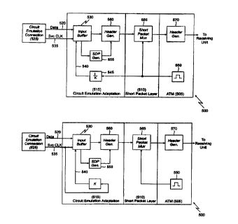
FIG. 5A illustrates the functional layers and elements of an exemplary
2 0 embodiment 500 of the present invention with respect to a
telecommunication system
sending unit. The three functional layers include the ATM layer 505, the short
packet
layer 510, and the circuit emulation adaptation layer 515. As previously
mentioned,
the present invention replaces the AAL 101 with a short packet layer and a
circuit
emulation adaptation layer.
The exemplary embodiment 500 operates as follows. Circuit emulation
data 520, from a particular circuit emulation connection 525, is clocked into
an input
buffer 530, located in the circuit emulation adaptation layer 515, by a
service clock
(SVC CLK) 535. The input buffer 530 is a hardware component comprising a
number
of shift registers which perform a serial to parallel conversion.
CA 02288873 1999-11-OS
WO 98/51114 PCT/SE98/00750
-6-
The SVC CLK 535 functions at a particular clock rate, and it may be
accompanied by a frame clock (not shown), if the circuit emulation data is
structured
data. The purpose of the frame clock is to identify the beginning of each data
frame.
Hence, the frame clock frequency will be a derivative of the service clock
frequency.
The circuit emulation adaptation layer 515 also includes a packetization
clock. More specifically, it includes a packetization clock signal 540. In one
embodiment, the packetization clock signal 540 is derived by applying a
frequency
divider 545 to the signal produced by the ATM cell shaping clock 550, which is
maintained in the ATM layer 505. As illustrated in FIG. 5A, the signal
produced by
1 o the ATM cell shaping clock 550 is divided by a value K, which is an
operator
adjustable variable. Therefore, the operator can control the period of the
packetization
clock by adjusting the value of K. Since the length of the short packets is a
function of
the packetization clock period, the operator can control the length of the
short packets
extracted from the input buffer 530. Note, the length of the short packets is
also a
function of the service clock rate. For example, as the packetization clock
period
increases, so too will the length of the short packets. Likewise, as the
service rate
increases, so too will the length of the short packets.
In a second embodiment, as illustrated in FIG. 5B, the packetization
clock signal 540 is derived by applying a factor K to the signal produced by
the SVC
2 o CLK 535. Again, the operator would be able to control the period of the
packetization
clock signal 540 by adjusting the value of K.
If the circuit emulation data is structured data, a sequence of short
packets will be passed from the input buffer 530 to a SDP generation unit 555.
The
SDP generation unit will produce a SDP which, as explained previously, is used
for
2 5 maintaining the alignment of data frames at the receiving unit. If the
circuit emulation
data is unstructured data, the sequence of short packets will be passed from
the input
buffer 530 directly to the header generation unit 560. The header generation
unit then
generates a header 420 for each short packet 405. The header may include, for
example, the SDP (if one is required), a sequence counter, a data type
identifier, and a
3 o circuit emulation connection identifier.
CA 02288873 1999-11-OS
WO 98/51114 PCT/SE98/00750
_7_
The sequence of short packets is then forwarded to the short packet
multiplexer 565. The short packet multiplexer then multiplexes the sequence of
short
packets containing circuit emulation data from circuit emulation connection
525 into the
ATM cell stream along with short packets containing data from other
connections (not
shown), including circuit emulation connections and/or connections carrying
other
types of traffic (e.g., control signals and compressed voice). Since the short
packet
multiplexer 565 multiplexes short packets from numerous connections, each of
which
may be sending short packets simultaneously, the order in which the short
packet
multiplexer 565 multiplexes the short packets is determined by a programmed
priority
1 o schedule, which defines the relative transmission priority for each short
packet. By
multiplexing circuit emulation data into a single ATM cell, with short packets
from
other connections, the present invention decreases overall transmission delays
and
increases bandwidth utilization.
It is well recognized by those skilled in the art that the ATM layer 505
can support several different kinds of bandwidth allocation, or traffic
service categories
such as constant bit rate (CBR) services, variable bit rate (VBR) services,
available bit
rate (ABR) services, and unspecified bit rate (UBR) services. In accordance
with a
preferred embodiment of the present invention, ATM cells are dispatched from
the
sending unit and constant, peak cell rate allocation is controlled by the ATM
cell
2 o shaping clock 550. Since the packetization clock signal 540 is derived
directly from
the ATM cell shaping clock 550, there is less potential for interference
between the
generation of short packets and the generation of ATM cells.
When the ATM cell shaping clock 550 signifies that the current ATM
cell is to be transported, a header generation unit 570 in the ATM layer 505
will cause
2 5 a standard ATM cell header to be appended to the payload of the current
ATM cell.
The ATM cell header and payload are then transported to the appropriate
receiving
unit. One of skill in the art will readily appreciate that the ATM cell could
transition
through a number of different ATM-switches before arriving at the desired
receiving
entity. Each of these ATM-switches would result in additional transportation
delays
3 o independent of the present invention.
CA 02288873 1999-11-OS
WO 98/51114 PCT/SE98/00750
_g_
FIG. 6 depicts the functional layers of the present invention, with respect
to the receiving unit, in accordance with an exemplary embodiment 600. As in
the
sending unit, the functional layers include an ATM layer 605, a short packet
layer 610,
and a circuit emulation adaptation layer 615. Again, the present invention
replaces the
AAL 101 with the short packet layer 610 and the circuit emulation adaptation
layer
615.
The exemplary embodiment 600 operates as follows. The ATM layer
605 receives an incoming ATM cell from the sending unit, wherein an ATM header
removal unit 620 removes the ATM cell header from the current incoming ATM
cell
l0 payload, and then passes the payload onto the short packet demultiplexer
625 located in
the short packet layer 610. The short packet demultiplexer 625 separates the
short
packet sequences according to their corresponding connections, which may
include one
or more circuit emulation connections. The short packets are then forwarded to
the
appropriate adaptation layer. Short packets containing circuit emulation data
are passed
to a circuit emulation adaptation layer, e.g., circuit emulation adaptation
layer 615.
In the circuit emulation adaptation layer 615, a short packet header
removal unit 630 removes the header from each short packet. The header removal
unit
630 is also responsible for extracting the SDP if the corresponding sequence
of short
packets contains structured data. The header removal unit 630 then sends the
short
2 o packets, and the SDP if the short packets contain structured data, to the
output buffer
635. The output buffer 635 utilizes the SDP to segment the blocks of data and
to
generate a block rate clock. For example, if standard PDH/SDH lines are being
emulated, the SDP will be used to identify 0.125 microsecond frame borders.
The
output buffer 635 is a hardware component comprising a series of shift
registers that
2 5 performs a parallel to serial data transformation.
The header removal unit 630 is also responsible for transmitting a clock
recovery initiation pulse to the clock recovery unit 640 if the corresponding
sequence
of short packets contains unstructured data. Whether the sequence of short
packets
contain structured or unstructured data, the clock recovery unit, in turn,
controls the
3 o rate at which data is transferred from the output buffer 635 to the
circuit emulation
CA 02288873 1999-11-OS
WO 98/51114 PCT/SE98/00750
-9-
connection 645. To accomplish this, the clock recovery unit 640 regenerates
(i.e.,
recovers) the rate of the service clock 535 so that the circuit emulation data
is
transferred to the corresponding circuit emulation connection 645 at the
required data
rate. The clock recovery unit can regenerate the service clock rate in a
number of
different ways.
The clock recovery unit 640, in a preferred embodiment, regenerates the
service clock rate by extracting the service clock rate from the ATM stream as
a
function of the ATM cell arrival rate distribution, wherein the ATM cell
arrival rate
distribution directly reflects the frequency of the ATM cell shaping clock
550. The
clock recovery unit 640 can then use the ATM cell arrival rate distribution
and the
value of K to determine the frequency of the packetization clock (P~LK) signal
540. The
clock recovery unit 640 then determines the rate of the service clock in
accordance with
the following relationship:
Z S SVCCLK - NVAR * PCLK - NVAR * SHcLK~K (1)
wherein SVC~LK represents the service clock rate, P~LK represents the
packetization
clock rate, SH~LK represents the shaping clock rate, and N"AR represents the
size of the
short packets. Because NypR can vary due to fluctuations in the frequency of
the
2 0 service clock and the frequency of the shaping clock SH cLK, a service
clock estimate is
smoothed by a low pass filter, thus helping to attenuate packet size fitter.
With respect to structured data, the service block rate is derived in
accordance with the following relationship.
2 5 SVCBLK = NVAR~NBLK * PCLK - NVAR~NBLK * SHCLK~~2)
The block size NBLK is derived in accordance with the SDP, which is extracted
by the
header removal unit 640 as explained above. The block rate is also independent
of
block size which implies that the number of time slots for standard circuit
emulation of
CA 02288873 1999-11-OS
WO 98/51114 PCT/SE98/00750
-10-
a PDH/SDH connection could be changed without dramatically re-synchronizing
the
service block-rate clock.
The clock recovery method described above is advantageous over prior
clock recovery methods because this method relies exclusively on the
characteristics of
the ATM Payer 605, which already accommodate for delay variations caused by
the
multiplexing of short packets. Accordingly, the clock recovery unit 640 can
more
accurately compute the service clock rate.
Nevertheless, the clock recovery unit 640 could recover the service
clock in accordance with any number of prior methods, particularly those most
often
1 o used in conjunction with AAL 1. In accordance with one such clock recovery
method,
the service clock is recovered from an external network clock. There is no
internal
clock recovery required with this method. Another prior method for recovering
the
service clock is the Adaptive Clock Recovery method. This method involves
measuring the average output buffer fill level, then utilizing the measurement
to adjust
the phase-locked loop (PLL) in the clock recovery unit 640. Yet another prior
technique for recovering the service clock is the Synchronous Residual Time
Stamp
method. This method involves measuring the difference between a stable system
clock
and the service clock, then using the measurement to adjust the PLL. These
methods
are well known in the art.
2 o Although each of the above-identified prior methods could be used for
clock recovery, there is less delay variation with the present invention. This
is due to
the fact that the packetization clock 540 is derived from the ATM cell shaping
clock
550, in at least one of the above-identified embodiments. Therefore, clock
recovery
performance is primarily dependent upon the transmission characteristics at
the ATM
2 5 layer 103 rather than the performance characteristics of the AAL.
FIG. 7 is a flowchart depicting the method steps for transporting low bit
rate, circuit emulation data from a sending unit to a receiving unit in
accordance with a
preferred embodiment of the present invention. As illustrated in block 705,
circuit
emulation data 520 is first shifted into an input buffer 530 in the circuit
emulation data
3 o adaptation layer 515 at a rate that is governed by the service clock 535.
The circuit
CA 02288873 1999-11-OS
WO 98/51114 PCT/SE98/00750
-11-
emulation data 520 is then segmented, if necessary, and packetized into one or
more
short packet payloads, as shown in block 710. Bit padding may be added, if
necessary,
as explained above, to maintain byte alignment. Segmentation and, therefore,
the size
of the short packet payloads are controlled by a packetization clock signal
540, which
is derived from an ATM cell shaping clock 550 in the ATM layer 505 or from
service
clock 535.
The next step depends upon whether the circuit emulation data 520 is
structured data or unstructured data, as illustrated by decision block 715. If
the circuit
emulation data 520 is structured data, in accordance with the "YES" path out
of
1 o decision block 715, the circuit emulation adaptation layer 515 will
generate a SDP, as
shown in block 720, which is subsequently used at the receiving unit to
maintain data
block andlor data frame alignment. The circuit emulation adaptation layer 515
then
generates a header for the one or more short packets, in accordance with block
725. If
the circuit emulation data 520 is not structured data, in accordance with the
"NO" path
out of decision block 715, the circuit emulation adaptation layer will simply
generate a
header, as shown in block 725, without first generating a SDP.
The generation of a SDP depends upon whether the circuit emulation
data is structured. Alternatively, the generation of a SDP may depend upon
whether
there is a fixed relationship between data packet size and block size. If
there is no
2 o relationship, then a SDP will be generated, as explained above, and as
illustrated in
FIG. 7B (blocks 750 and 760). If, however, there is a fixed relationship
between data
packet size and block size, then the function of the SDP can be accomplished
by setting
a system configuration command, for example, through software controls, as
illustrated
in FIG. 7B (blocks 750 and 755). By not generating and transporting a SDP,
valuable
2 5 bandwidth is preserved for data and/or other important overhead
information.
Once the headers have been generated for the one or more short packets,
the header and the packetized data are then forwarded to the short packet
layer 510,
wherein the packetized data is multiplexed together with short packets
generated by
other connections, as illustrated in block 730. As mentioned above, the order
in which
3 o the short packets from each connection are multiplexed into the ATM stream
will
CA 02288873 1999-11-OS
WO 98/51114 PCT/SE98/00750
-12-
depend upon a preestabiished priority schedule. ATM cells are then formed and
dispatched to the desired receiving unit as a function of the ATM cell shaping
clock
550, in accordance with block 735.
FIG. 8 is a flowchart depicting the method steps for receiving ATM cells
at a receiving unit and for extracting the low bit rate, circuit emulation
data from the
sequence of short packets so that it can be properly forwarded to the circuit
emulation
connection 645, in accordance with a preferred embodiment of the present
invention.
The method illustrated in FIG. 8 proceeds as follows. In accordance
with block 805, an ATM cell is received by the ATM layer 605, which removes
the
1 o ATM cell header and forwards the ATM cell payload to the short packet
layer 610.
The short packets are then demultiplexed by the short packet demultiplexer 625
according to their respective circuit emulation connections, as illustrated by
block 810.
The short packet demultiplexer 625 then forwards each sequence of short
packets to a
corresponding circuit emulation adaptation layer 615, where the headers are
removed
for each short packet, in accordance with block 815. The corresponding short
packet
payloads are then directed to an output buffer 635, as shown in block 820, and
a clock
recovery trigger signal is issued to initiate the process of recovering the
service clock
(i.e., regenerating the service clock rate), as shown in block 825. Once the
service
clock has been recovered, the circuit emulation adaptation layer 615 will
forward the
2 o circuit emulation data from the output buffer 635 to the circuit emulation
connection
645, at the appropriate service rate, in accordance with block 830. It should
be noted
that the service clock can be recovered in accordance with any one of a number
of
different methods as explained above. However, in a preferred embodiment, the
service clock is extracted as a function of the ATM layer characteristics, as
explained
2 5 above.
The present invention has been described with reference to a preferred
embodiment. However, it will be readily apparent to those skilled in the art
that it is
possible to embody the invention in specific forms other than the preferred
embodiment
described above. This may be done without departing from the spirit of the
invention.
3 o The preferred embodiment is illustrative and should not be considered
restrictive in any
CA 02288873 1999-11-05
WO 98/51114 PCT/SE98/00750
-13-
way. The scope of the invention is given by the appended claims, rather than
the
preceding description, and all variations and equivalents which fall within
the range of
the claims are intended to be embraced therein.