Note: Descriptions are shown in the official language in which they were submitted.
CA 02289085 1999-11-04
WO 98/53645 PCT/US98/06119
ELECTROLUMINESCENT DEVICE AND
METHOD FOR PRODUCING THE SAME
Field of the Invention
The present invention relates to an electroluminescent device (hereinafter
referred to as "EL device") having a luminescent layer comprising luminescent
particles and a matrix resin. In particular, the present invention relates to
an EL
device with high luminance which is based on the concept different from that
of
conventional "dispersion type luminescent layers".
Backeround of the Invention
EL devices comprising a so-called 'dispersion type luminescent layer"
which is formed by dispersing luminescent particles such as fluorescent
substances
in a matrix resin such as a polymer having a high dielectric constant are
known
from the following publications:
For example, JP-B-59-14878 discloses an EL device comprising a
transparent substrate, a transparent electrode layer, an insulating layer
consisting of
a vinylidene fluoride base matrix resin, a luminescent layer comprising a
vinylidene fluoride base matrix resin and fluorescent particles, the same
insulating
layer as above, and a rear electrode, which are laminated in this order.
JP-B-62-59879 discloses an EL device comprising a polyester film, an ITO
electrode, a luminescent layer comprising a cyanoethylated ethylene-vinyl
alcohol
copolymer (a matrix resin) and fluorescent particles, and an aluminum foil (a
rear
electrode), which are laminated in this order.
Summary of the Invention
However, such the "dispersion type luminescent layers" can hardly increase
the luminance, because the luminescent particles having a larger specific
gravity
than the matrix resin tend to sink in a paint for forming a luminescent layer
comprising the luminescent particles dispersed in the matrix resin solution
and
CA 02289085 1999-11-04
WO 98/53645 PCT/US98/06119
therefore, it is difficult to disperse the luminescent particles uniformly in
the matrix
resin in the luminescent layer formed from such the paint.
Furthermore, the dispersibility deteriorates when the amount of the
luminescent particles in the paint is increased for increasing the filling
rate of
luminescent particles in the luminescent layer. Thus, the added amount of the
luminescent particles is limited.
In addition, it is relatively difficult to increase a coating thickness of the
luminescent layer with a uniform thickness using such the dispersion type
paint.
Therefore, the number of applications of the paint should be increased to
increase
the thickness of the luminescent layer for increasing the luminance, the
productivity decreases, and it is difficult to produce a sheet-form EL device
having
a large area.
One object of the present invention is to provide an EL device with an
increased filling rate of luminescent particles in a luminescent layer and
significantly improved luminance for solving the above problems of the
conventional devices.
Another object of the present invention is to provide a method for
producing an EL device which can produce a sheet-form EL device having a high
luminance and a large area at a high productivity without using the above
dispersion type paint.
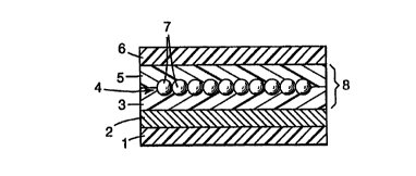
According to the first aspect (and with reference to Fig. 1.), the present
invention provides an electroluminescent device comprising:
a) a transparent substrate ( 1 ),
b) a transparent conductive layer (2) placed on the back surface of said
transparent substrate ( 1 ),
c) a luminescent layer (8) comprising luminescent particles (7) and a
matrix resin and being placed on the back surface of said transparent
conductive
layer (2), and
d) a rear electrode (6) placed on the back surface of said luminescent
layer (8),
wherein said luminescent layer (8) comprises
-2-
CA 02289085 1999-11-04
WO 98/53645 PCT/US98/06119
(c-1) a transparent support layer (3) comprising a matrix resin and being
placed on the side of said transparent conductive layer (2),
(c-2) an insulating layer (5) comprising an insulating material and being
placed on the side of said rear electrode, and
(c-3) a luminescent particle layer (4) consisting essentially of particles
which comprise luminescent particle (7) and are embedded in both said support
layer (3) and said insulating layer (S).
According to the second aspect, the present invention provides a method for
producing an electroluminescent device which comprises a transparent substrate
( 1 ), a transparent conductive layer (2) placed on the back surface of said
transparent substrate ( 1 ), a luminescent layer (8) comprising luminescent
particles
(7) and a matrix resin and being placed on the back surface of said
transparent
conductive layer (2) and a rear electrode (6) placed on the back surface of
said
luminescent layer (8), which method comprises the steps of:
i) providing a transparent substrate ( 1 ) on one surface of which a
transparent conductive layer (2) is laminated,
ii) applying a paint for forming a support layer {3) containing a matrix
resin on said transparent conductive layer (2),
scattering particles containing luminescent particles (7) in a layer state and
embedding a part of each particle in said paint prior to solidification of
said paint,
solidifying said paint and forming a transparent support layer (3) and a
luminescent particle layer (4) bonded to said support layer (3),
iii) applying a paint for forming an insulating layer (5) comprising an
insulating material on said luminescent particle layer (4), solidifying said
paint and
forming said insulating layer (5) bonded to said luminescent particle layer
(4), and
iv) laminating a rear electrode (6) on said insulating layer (5).
In the EL device of the present invention, the luminescent particle layer (4)
contained in the luminescent layer (8) comprises substantially the particles
containing the luminescent particles, and is placed between the support layer
(3)
and the insulating layer (5) and bonded to the both layers. Therefore, the
filling
-3-
CA 02289085 1999-11-04
WO 98/53645 PCTlUS98/06119
rate of the luminescent particles in the luminescent layer (8) increases, and
the
luminance increases considerably.
Furthermore, when the EL device is produced by the method of'he present
invention comprising the steps i) through iv), it is not necessary to use the
dispersion type paint of luminescent particles unlike the conventional
techniques,
and the sheet-form EL device having the high luminance and the large area can
be
produced at a high productivity.
Brief Description of the Drawing
Fig. 1 is a cross-sectional view of one EL device of the present invention.
Embodiments of the Invention
Fig. 1 shows a cross section of an example of the EL device according to
the present invention having the following numerals and elements:
1: Transparent substrate, 2: transparent conductive layer, 3: support layer,
4:
luminescent particle layer, 5: insulating layer, 6: rear 30 electrode, 7
luminescent
particles, 8: luminescent layer.
EL Device
The EL device comprises a laminate having a transparent substrate ( 1 ) and
a transparent conductive layer (2), a rear electrode (6) and a luminescent
layer (8)
placed between this laminate and the rear electrode (8). The structure of the
EL
device of this form is substantially the same as that of the conventional
dispersion
type EL device except the structure of the luminescent layer (8).
The luminescent layer (8), which will be explained in detail below, has a
structure in which the transparent support layer (3) comprising the matrix
resin, the
insulating layer containing the insulating material, and the luminescent
particle
layer (4) placed between the layers (3) and (5), which are laminated in close
contact.
In general, the thickness of the whole EL device is in the range between 50
and 3000 Vim.
-4-
CA 02289085 1999-11-04
WO 98/53645 PCT/LTS98/06119
Transparent substrate
The transparent substrate may be the same as that used in the dispersion
type EL devices, and for example, glass plates, plastic films and the like can
be
used. Examples of the plastic films are films of polyester resins such as
polyethylene terephthalate (PET), polyethylene naphthalate (PEN), etc.;
acrylic
resins such as polymethyl methacrylate, modified polymethyl methacrylate,
etc.;
fluororesins such as polyvinylidene fluoride, acryl-modified polyvinylidene
fluoride, etc.; polycarbonate resins; vinyl chloride resins such as vinyl
chloride
copolymers; and the like.
The transparent substrate may be a single layer film as shown in Fig. l,
while it may be a multilayer film. For example, whiteness of the light can
increase,
when at least one layer of the multilayer film has high transparency and
contains a
dye which develops a complimentary color to a color emitted by the luminescent
layer. Preferably, examples of such the dye are red or pink fluorescent dyes
such
as rhodamine 6G, rhodamine B, perylene dyes, etc. when the emitted light from
the
luminescent layer is blue-green.
The both surfaces of the transparent substrate are usually flat, while the
surface which is not in contact with the transparent conductive layer may have
prismatic projections unless the effects of the present invention are
impaired.
The light transmission through the transparent substrate is usually at least
60%, preferably at least 70%, in particular at least 80%. "Light transmission"
means a transmission of light measured according to JAPANESE INDUSTRIAL
STANDARD K 7105 using light of 550 nm.
The transparent substrate may contain additives such as UV light absorbers,
moisture absorbents, colorants, fluorescent materials, phosphors, and the like
unless the effects of the present invention are impaired.
Transparent conductive layer
The transparent conductive layer is placed on the back surface of the
transparent substrate in close contact therewith.
-5-
CA 02289085 1999-11-04
WO 98/53645 PCT/US98/06119
The transparent conductive layer may be any transparent electrode which is
used in the dispersion type EL devices such as an ITO (Indium-Tin Oxide) film,
and the like. The thickness of the transparent conductive layer is usually
between
0.1 and 1000 Vim, the surface resistivity is usually between 1000 and 500
S2/square,
preferably between 200 and 300 S2/square. The light transmission is usually at
least 70%, preferably at least 80%.
The ITO film is formed by any conventional film-forming method such as
vapor deposition, sputtering, paste coating, and the like.
The ITO film is formed directly on the transparent substrate in the
embodiment of Fig. 1, while a primer layer may be formed on the transparent
substrate, and then the ITO film may be formed on the primer layer. In place
of the
primer layer, the surface of the transparent substrate is treated with corona,
and the
like for facilitating the adhesion of the ITO film. Alternatively, the ITO
film is
formed on the luminescence layer and then the transparent substrate is
laminated
on the ITO film.
The rear electrode layer is placed on the back surface of the luminescent
layer, that is, the side facing the insulating layer. The rear electrode is in
direct
contact with the luminescent layer in the embodiment of Fig. 1.
A resin layer can be provided between the rear electrode and the
luminescent layer for increasing the adhesion between them. The resin for the
resin layer may be a polymer with a high dielectric constant, which will be
explained below. The resin layer may contain insulating organic particles.
The rear electrode may be a conductive film used in the dispersion type EL
devices such as a metal film of aluminum, gold, silver, copper, nickel,
chromium,
etc.; a transparent conductive film such as an ITO film; and the like. The
metal
film may be a vapor deposited film, a sputtered film, a metal foil, and the
like.
The thickness of the rear electrode is usually between S and 1 000 ~.m.
The EL device can emit light from both surfaces when the rear electrode
consists of the transparent conductive film and the insulating layer is
transparent.
-6-
CA 02289085 1999-11-04
WO 98!53645 PCTNS98/06119
Support layer
The support layer for the luminescent layer is placed preferably on the back
surface of the transparent conductive layer in close contact therewith, and
thereby
the luminescent efficiency of the luminescent layer is easily increased.
The support layer is a transparent layer containing a matrix resin. The
thickness of the supped layer is usually between 5 and 1000 Vim, and the light
transmission is usually at least 70%, preferably at least 80%.
The matrix resin may be a resin which is used in the dispersion type EL
devices such as epoxy resins, polymers having a high dielectric constant, and
the
like. The polymers having the high dielectric constant are those having a
dielectric
constant of usually at least about 5, preferably between 7 and 25, more
preferably
between 8 and 18, when it is measured by applying an alternating current of 1
kHz.
When the dielectric constant is too low, the luminance may not increase. When
it
is too high, the life of the luminescent layer tends to shorten.
Examples of the polymers having the high dielectric constant are vinylidene
fluoride resins, cyanoresins, and the like. For example, the vinylidene
fluoride
resin may be obtained by copolymerization of vinylidene fluoride and at least
one
other fluorine-containing monomer. Examples of the other fluorine-containing
monomer are tetrafluoroethylene, trifluorochloroethylene, hexafluoropropylene,
and the like. Examples of the cyano-resin are cyanoethylcellulose,
cyanoethylated
ethylene-vinyl alcohol copolymer, and the like.
The support layer consists of the matrix resin in the embodiment of Fig. l,
while it may contain additives such as other resins, fillers, surfactants, UV
light
absorbers, antioxidants, anti-fungus agents, rust-preventives, moisture
absorbents,
colorants, phosphors, and the like, unless the effects of the present
invention are
impaired. For example, the support layer may contain red or pink fluorescent
dyes
such as rhodamine 6G, rhodamine B, perylene dyes, and the like, when the
emitted
light from the luminescent particle layer is blue-green. Furthermore, the
above
other resins may be curable or tacky.
_7-
CA 02289085 1999-11-04
WO 98/53645 PCT/US98/06119
Insulatin;~ layer
The insulating material contained in the insulating layer of the luminescent
layer may be insulating particles, polymer having a high dielectric constant,
and
the like, which are used in the dispersion type EL devices.
The insulating layer in the embodiment of Fig. 1 is a coating layer formed
from a paint which has been prepared by dispersing the insulating particles in
the
polymer having the high dielectric constant. Examples of the insulating
particles
are insulating inorganic particles of, for example, titanium dioxide, barium
titanate,
and the like. The polymers having the high dielectric constant may be the
polymers used for the support layer.
The insulating layer may be formed by coating the paint on either the rear
electrode or the luminescent particle layer.
When the insulating layer is the coating layer comprising the insulating
particles and the polymer having the high dielectric constant, the amount of
the
insulating particles is between 1 and 400 wt. parts, preferably between 10 and
300
wt. parts, more preferably between 20 and 200 wt. parts, per 100 wt. parts of
the
polymer having the high dielectric constant. When the amount of the insulating
particles is too low, the insulating effect decreases, and thus the luminance
tends to
decrease. When the amount is too high, the application of the paint may be
difficult.
The thickness of the insulating layer is usually between 5 and 1000 Vim.
The insulating layer may contain additives such as fillers, surfactants,
antioxidants,
antifungus agents, rust-preventives, moisture absorbents, colorants,
phosphors,
curable resins, tackifiers, and the like, insofar as the insulating properties
are not
impaired.
Luminescent particle layer
The luminescent particles in the luminescent particle layer spontaneously
emit light when they are placed in an alternating electric field. As such the
particles, fluorescent particles which are used in the dispersion type EL
devices can
be used. Examples of the fluorescent materials are single substances of
fluorescent
_g_
CA 02289085 1999-11-04
WO 98/53645 PCT/US98/06119
compounds {e.g. ZnS, CdZnS, ZnSSe, CdZnSe, etc.), or mixtures of the
fluorescent
compounds and auxiliary components (e.g. Cu, I, C1, AI, Mn, NdF~, Ag, B,
etc.).
The average particle size of the fluorescent particles is usually between 5
and 100 Vim. The particulate fluorescent materials on which a coating film of
glass, ceramics, and the like is formed may be used.
The thickness of the luminescent particle layer is usually between 5 and
500 pm. When the fluorescent particle layer consists of a plurality of
particles
which are placed in a single layer state, the EL device can be made thin
easily.
Furthermore, the luminescent particle layer may contain at least two kinds
of luminescent particles. For example, at least two kinds of luminescent
particles
which emit blue, blue-green or orange light and have discrete spectra each
other are
mixed, and thus a luminescent layer having the high whiteness can be formed.
The content of the luminescent particles in the luminescent particle layer is
preferably at least 40 wt. %. When the content is less than 40 wt. %, the
effects for
improving the luminance may decrease. The luminance can be maximized when
the particles consist of the luminescent particles. Accordingly, the
particularly
preferable content of the luminescent particles is between 50 and 1 00 wt. %.
The luminescent particle layer may contain one or more kinds of particles
other than the luminescent particles, for example, particles of glass,
coloring
materials, phosphors, polymers, inorganic oxides, and the like. For example,
luminescent particles which emit blue-green light and a pink-coloring material
which is the complimentary color to blue-green (e.g. particles containing
rhodamine 6G, rhodamine B, etc.) are mixed for forming the luminescent layer
having the high whiteness.
Formation of luminescent layer
The laminate structure of the luminescent layer comprising the support
layer, luminescent particle layer and insulating layer may be formed as
follows:
Firstly, the luminescent particle layer is formed on the surface of either the
support layer or the insulating layer by any conventional powder coating
method.
-9-
CA 02289085 1999-11-04
WO 98/53645 PCT/US98/06119
For example, particles containing the luminescent particles are. scattered on
the substrate layer while it maintains flowability, by a suitable method such
as
static suction, spraying, gravimetric scattering, and the like, and the
luminescent
particle layer in which a part or whole of the particles are embedded in the
support
layer is formed. After that, the flowability of the support layer is
suppressed, and
the support layer and the particle layer are bonded. For maintaining the
flowability
of the support layer, following methods are preferable: A method for
maintaining
the undried state of the coating layer formed from the paint for the support
layer
containing the solvent, A method for maintaining the support layer at a
temperature
higher than the softening or melting point of the resin for the support layer,
and A
method for adding a radiation-curable monomer to the paint for the support
layer.
These methods make a solidifying procedure for suppressing the flowability of
the
support layer (drying, cooling or hardening) easy.
In the same way, the luminescent layer can be formed on the insulating
layer made of the coating layer.
The final layer (either the support layer or the insulating layer) is
laminated
on the luminescent particle layer which has been formed as above, and the
laminate
structure in which the three layers are bonded is formed. The final layer is
preferably laminated by coating a paint containing materials for forming the
final
layer and solidifying it, or by press-bonding a film made of materials for
forming
the final layer. These methods can surely form a bonded structure without the
presence of any bubble at the interface between each pair of the support
layer,
luminescent particle layer and insulating layer.
The luminescent particle layer consists of a plurality of particles which are
placed in a single layer state and is bonded to both the support and
insulating
layers, in the embodiment of Fig. 1. However, the luminescent particle layer
may
be a multilayer, or a part or whole of the particles may be embedded entirely
in
either the support layer or the insulating layer. It is important to form a
bonded
structure in which the luminescent particle layer is placed between the
support
layer and the insulating layer, and no bubbles are present at the interface
between
each pair of the layers.
-10-
__.~ ~ _. __ 1.
__
CA 02289085 1999-11-04
WO 98/53645 PCT/US98/06119
In the luminescent particle layer formed as above, the materials of the
support or insulating layer penetrate in spaces between the particles. In such
the
case, a filling rate of the particles is usually at least 20 voi. %,
preferably at least 30
vol. %, more preferably at least 40 vol. %, since the decrease of the filling
rate may
lead to the decrease of luminance.
Herein, the "filling rate of particles" is defined as a percentage of the
total
volume of the particles in the volume of a hypothetical layer comprising all
the
particles in the luminescent particle layer and the materials which are
present
between the particles.
Furthermore, each of the support and insulating layers may be a laminate of
two or more layers, unless the effects of the present invention are impaired.
Production of EL device
Now, the production method of the present invention, which is suitable for
the production of the above described EL device, will be explained.
Firstly, the transparent substrate, on which surface the transparent
conductive layer has been laminated, is provided. A paint for forming the
support
layer is applied on the transparent conductive layer. After that, particles
containing
the luminescent particles are scattered in a layer state over the applied
paint prior to
drying of the paint, and the particle layer is partly embedded in the support
layer,
followed by drying of the paint. These steps can easily form the luminescent
particle layer which is partially embedded in and bonded to the support layer.
The particles are embedded in the support layer so that usually 1 to 99 %,
preferably 10 to 90 %, more preferably 20 to 80 % of the size of each particle
in
the vertical direction (to the plane of the support layer) is embedded in the
support
layer. When the embedded percentage is less than 1 %, the particle layer tends
to
be damaged during the formation of the insulating layer. When the particles
are
embedded so that the embedded percentage exceeds 99 the particle layer may not
be formed uniformly.
The coating thickness of the paint for forming the support layer is selected
so that the dry thickness of the support layer is in the above range. The
solid
-11-
CA 02289085 1999-11-04
WO 98/53645 PCT/US98/06119
content in the paint for forming the support layer is usually between 5 and 80
wt.
%. A solvent used in the paint is selected from conventional organic solvents
so
that the matrix resin is homogeneously dissolved.
The paint may be prepared with mixing or kneading apparatuses such as
homomixers, sand mills, planetary mixers, and the like.
For applying the paint, coating apparatuses such as bar coaters, roll coaters,
knife coaters, die coaters, and the like can be used.
The drying conditions depend on the kind of solvent in the paint and the
solid content of the paint, and usually include a temperature in the range
between
room temperature (about 25°C) and I50°C, and a drying time in
the range between
5 seconds and 1 hour.
The particles are scattered by the above method within one minute from the
application of the paint for forming the support layer, which makes the
embedding
of particles easy. The drying degree of the paint depends on the wettability
between the particles and the support layer, and is usually in the range
between 10
and 95 wt. %, preferably between 20 and 90 wt. % in terms of the solid
content.
Subsequently, the paint for forming the insulating layer is applied so that
the luminescent particle layer is covered, and dried. Accordingly, a bonded
structure, in which the luminescent particle layer is embedded in both the
support
and insulating layers and no bubble is present at the interface between each
pair of
the layers, is formed.
The coating thickness of the paint for forming the insulating layer is
selected so that the dry thickness of the insulating layer is in the above
range.
The solid content in the paint for forming the insulating layer is usually
between 5 and 70 wt. %. A solvent used in the paint is selected from
conventional
organic solvents so that the insulating material is homogeneously dissolved or
dispersed.
This paint may be prepared and applied using the same apparatuses or tools
as those used for preparing and applying the paint for forming the support
layer.
The drying conditions depend on the kind of solvent in the paint and the
solid content of the paint, and usually include a temperature in the range
between
-12-
_ _T __...._._ ~__T
CA 02289085 1999-11-04
WO 98/53645 PCT/US98/06119
room temperature (about 25°C) and 1 SO°C, and a drying time in
the range between
seconds and 1 hour.
Finally, the rear electrode is laminated on the insulating layer. The rear
electrode may be formed by the above described methods. Among them, the
methods for forming thin films in vacuum such as the vapor deposition and
sputtering are preferable for effectively forming the rear electrode on the
insulating
layer, which has been dried after drying, with good adhesion between the rear
electrode and the insulating layer.
The steps of the above described production method are substantially the
same as those of a conventional method for producing a sheet-form product.
Therefore, the sheet-form EL devices having a high luminance and a large area
can
be produced at high productivity using the production steps for the
conventional
sheet-form products. Furthermore, the problems caused by the use of dispersion
paints are solved, since the above method does not use the dispersion paints
of the
luminescent particles unlike the production of the dispersion type EL devices.
The EL devices may be produced by an alternative method which may
analogous to the above method, comprising applying the paint for the
insulating
layer on the support including the rear electrode, scattering the luminescent
particles prior to drying of the applied paint, embedding a part of the
particle layer
in the insulating layer, then, drying the paint for the insulating layer,
applying and
drying the paint for the support layer, and finally laminating the transparent
substrate which carries the transparent conductive layer. This method has the
same
effects as the above described method.
Application of EL device
The EL device of the present invention can be used as a back-light source
for liquid crystal displays such as liquid crystal instrument panels of
automobiles.
In addition, the EL device of the present invention can be used as a light
source for
internal-illuminating type displays such as billboards, road signs, decorative
displays, and the like.
-13-
CA 02289085 1999-11-04
WO 98/53645 PCT/US98/06I19
For example, images such as characters, designs, and the like are printed on
the surface of a light-transmitting sheet, and the sheet is placed on the EL
device
with the back surface of the sheet facing the light-emitting side of the EL
device.
The light-transmitting sheet may be made of the same material as that of the
above
transparent substrate, and has a light transmission of at least 20 %. In this
case, the
back surface of the sheet and the light-emitting side of the EL device are
preferably
bonded each other. To this end, a light-transmitting adhesive is used.
Examples of
such the adhesive are pressure-sensitive acrylic adhesives, heat-sensitive
acrylic
adhesives, and the like.
Alternatively, an EL device built-in type display can be assembled by using
the light-transmitting sheet as the above transparent substrate, forming the
transparent conductive layer directly on the back surface of the light-
transmitting
sheet, and laminating the luminescent layer on the conductive layer.
Furthermore, a prism type retroreflective sheet may be used as the light-
transmitting sheet (or the transparent substrate). The combination with the
retroreflective sheet can impart both the retroreflectivity and the self light-
emitting
properties to the EL device built-in type display.
Light is emitted from the EL device by connecting two terminals, which are
in connection with the transparent conductive layer and the rear electrode
layer,
respectively, to a power source, and applying a voltage to the EL device.
As the power source, cells such as dry cells, batteries, solar cells, etc. may
be used, or an alternating current is supplied to the EL device from a power
line
through an inventor, which alters the voltage or frequency, or change the
current
between the alternating current and the direct current. The applied voltage is
usually between 3 and 200 V.
The EL device of the present invention has the high light-emitting
ef~'iciency,
and therefore emit light with sufficient luminance (for example, 50 cd/m2 or
higher)
at a lower voltage (for example, 100 V or lower) than that necessary for the
conventional dispersion type ones .
-14-
SUBSTTME SHEET (RULE 26)
_ ~~_. ____._ ~____.___ _ __ ___. _____.._.._ __ T
CA 02289085 1999-11-04
WO 98/53645 PCT/US98/06119
When the EL device is used outdoors, it is preferably covered with water-
capturing films made of, for example, polyamide resins, or moistureproof films
made of, for example, polytetrafluoroethylene.
Example 1
Production of EL device
An ITO/PET laminate film (trade name: TCF-KPC 300-75 (A)
manufactured by OIKE Industries, Ltd.) (thickness, 75 pm; light transmission,
81 %) was used as a transparent substrate having an ITO layer. This film had a
transparent conductive layer of ITO which had been laminated by sputtering on
one surface of the film. The ITO layer has a thickness of 550 nm and a surface
resistivity of 250 12/square.
Separately, a paint for forming a support layer was prepared by mixing and
uniformly dissolving a polymer having a high dielectric constant (a
tetrafluoroethylene-hexafluoropropylene-vinylidene fluoride copolymer; trade
name "THV 200 P" having a dielectric constant of 8 (at 1 kHz) and a light
transmission of 96%) in ethyl acetate with a homomixer. The solid content of
the
paint was about 25 wt. %.
The paint for forming the support layer was applied on the transparent
conductive layer which was laminated on the transparent substrate. Luminescent
particles were scattered over the applied paint in substantially the single
layer state
prior to drying of the paint, and embedded in the paint so that about 50% of
the
diameter sunk. After that, the paint was dried. The paint was applied with a
notched bar at a barset of 50 Vim, and the particles were scattered
immediately after
the application of the paint. The drying conditions included a temperature of
about
65°C and a drying time of about one minute. The luminescent particles
were ZnS
luminescent particles (trade name: S-728 manufactured by OSRAM SYLVANIA;
average particle size, about 23 p,m).
Next, a paint for forming an insulating layer was applied so that the paint
covered the luminescent particle layer and dried, and an insulating layer was
formed. Thereby, a bonded structure, in which the luminescent particle layer
was
-15-
CA 02289085 1999-11-04
WO 98/53645 PCT/US98/06119
embedded both in the support and insulating layers and substantially no
bubbles
were present at interfaces between each pair of layers, was formed.
The paint for forming the insulating layer was prepared in the same manner
as that for the paint for forming the support layer except that a polymer
having a
high dielectric constant (THV 200 P described above), insulating particles
(barium
titanate manufactured by KANTO KAGAKU) and ethyl acetate were mixed. The
weight ratio of the polymer to the insulating particles was 100:80, and the
solid
content of the paint was about 38 wt. %. The paint was applied with a notched
bar
at a barset of 100 pm, and the drying conditions included a temperature of
about
65°C and a drying time of about one minute.
Finally, a rear electrode layer made of aluminum was laminated on the
insulating layer by vacuum deposition, and a film-form EL device of the
present
invention was obtained. In this step, the vacuum deposition was carried out
using a
vacuum deposition apparatus "EBV-6DA" (manufactured by ULVAC) under
reduced pressure of 10-5 Torr or less for 5 seconds.
Light emission from EL device
Respective terminals were attached to the transparent conductive layer and
the rear electrode layer of the EL device of this Example (prepared by cutting
the
above sheet-from device in a square of 100 mm x 100 mm), and were joined to a
power source (PCR SOOL manufactured by KIKUSUI ELECTRONIC
INDUSTRIES, Ltd.). Then, the alternating voltage was applied to the device
under
two sets of conditions (condition A: 100 V, 400 Hz; condition B: 120 V, 600
Hz).
The EL device emitted Iight uniformly under the both conditions.
The EL device was placed in a dark room, and the luminance was measured
at a distance of 1 meter from the surface of the transparent substrate using a
luminance meter (LS 110 manufactured by MINOLTA). The results are shown in
Table 1.
-16-
~ _
CA 02289085 1999-11-04
WO 98/53645 PCT/US98/06119
Comparative Example 1
An EL device was produced in the same manner as in Example I except
that a "dispersion type" luminescent layer was used.
The "dispersion type" luminescent layer was formed as follows:
The same polymer having the high dielectric constant as used in Example 1
( I 00 wt. parts), fluorescent particles ( 150 wt. parts) and ethyl acetate
were mixed
and dispersed with a homomixer, and a paint for forming a luminescent layer
was
obtained. The solid content of the paint was about 45 wt. %. The paint was
applied
on the transparent conductive layer of the transparent substrate using a
notched bar
at a barset of 80 Km, and dried at about 65°C for about one minute.
The luminance of the EL device of this Example was measured in the same
manner as in Example I . The results are shown in Table I .
Example 2.
I 5 An EL device was produced in the same manner as in Example 1 except
that ZnS fluorescent particles (S-723 manufactured by OSRAM SYLVANIA) was
used as fluorescent particles. The luminance of the EL device of this
Examplewas
measuredin the same manner as in Example I . The results are shown in Table 1.
Example 3
An EL device was produced in the same manner as in Example I except
that a cyanoresin (CR-M 723 manufactured by SHINETSU CHEMICAL) was used
as a polymer having a high dielectric constant for the support and insulating
layers.
The luminance of the EL device of this Example was measured in the same manner
as in Example 1. The results are shown in Table 1.
-17-
CA 02289085 1999-11-04
WO 98/53645 PCT/US98/06119
Table 1
Polymer having Luminance
(cd/m2)
high dielectricFluorescentConditionCondition
constant particles A B
Example THV 200P S-728 52.2 105.7
1
Example THV 200P X-723 58.9 98.8
2
Example CR-M S-728 85.3 146.7
3
C. Ex. THV 200P S-728 26.0 44-4
1
Effects of the invention
The present invention can easily increase the filling rate of the luminescent
particles in the luminescent layer, and provide the EL devices having the
luminance which is at least about 2 times larger than that of the dispersion
type EL
device.
The present invention can produce the sheet-form EL devices having a
large area and a high luminance at a high productivity without using any
dispersion
paint for forming a luminescent layer. According to the present invention, the
sheet-
form EL devices having the large area can be mass-produced by supplying a
rolled
transparent substrate sheet having a width of 25 to 200 cm and a length of 100
to
20,000 m and successively laminating tie transparent conductive layer, support
layer, luminescent particle layer, insulating layer and rear electrode.
-18-