Note: Descriptions are shown in the official language in which they were submitted.
CA 02289192 1999-11-03
SPECIFICATION
Communication DMA Device
Technical Field
The present invention relates to a communication DMA device, and
more specifically to a communication DMA device that frees the data bus
from the CPU and allows image data stored in a DRAM to be output via a
communication channel in outputting image data of an image taken by a
digital still camera to a personal computer.
Background AW
Normally, in a digital still camera, image data of an image taken can
be stored in a DRAM, and the CPU can read the stored image data and
transfer the data to a recording medium to be saved as an image, or the
data can be transferred to a display device to project the image. A DRAM
can utilize the area other than the image data area as a work area for
various processing. For instance, when image data is transferred to a
personal computer by serial communication interface, a recording medium
stores image data usually compressed in JPEG format, image data of a
suitable size for transmission is read therefrom and is temporarily written
into the work area of the DRAM, and thereafter the CPU reads the image
data as transmission data and writes the data into a communication circuit,
thereby the transmission data is serially output.
When the transmission of all image data to the work area is
completed by repeating the above processing, image data of a suitable size
for next transmission is read out and is written into the DRAM, and the
same processing as above is repeated to continue the transmission.
In order to speed up the communication, however, the CPU must be
monopolized by the communication control so that other processing cannot
be performed during this time. In addition, the CPU seldom controls a
camera using a 8 bit bus, but generally controls it using a 16 bit to 32 bit
bus.
-1-
CA 02289192 2002-09-25
On the other hand, communication processing generally involves a unit of
8 bits, and the well-known asynchronous/synchronous communication chip 8251
is also processed by 8 bits. Therefore, supposing that the CPU that controls
utilizes a 32 bit bus, the data is divided into 4 bytes, i. e. bits 7 to 0, 15
to 8, 23 to
S 16, and 31 to 24. Although the data of bits 7 to 0 can be directly written
into the
communication circuit, data from bits 31 to 8 must be written into the
communication circuit after being allocated again to bits 7 to 0. Thus, a
greater
load is imposed upon the CPU than when 32 bits of data is transferred at once,
and as a result, the processing speed of the CPU becomes slower. In
particular,
when transferring image data directly from the camera to a printer, a very
high-
speed transmission is required, which has surpassed the processing capability
of
the CPU.
The prior art have proposed various means to attempt to improve DMA
transfer capacity. For instance, Japanese Publication No. JP 64-76356,
published on March 22, 1989 discloses a system which transforms the data
transfer into words within an internal bus to halve the data frequency.
Furthermore, Japanese Publication No. JP 7-334451 to Osami, published
on December 22, 1995 discloses a DMA controller system that includes a timing
controller to control the timing of data transfer between an I/O device and a
memory.
However, the above prior art suffers from the disadvantage that it imposes
a processing load on the CPU, and does not provide for very high speed
transmission from Tnput/Output devices, such as transferring data from a
digital
camera directly to a printer.
Thus, the present invention provides a communication DMA device that
lightens the load for the CPU while allowing a high-speed transfer.
Disclosure of the Invention
The present invention is a communication DMA device, with a CPU, a
communication circuit and a memory sharing a data bus, for outputting to the
outside via the communication circuit transmission data stored in the memory;
-2-
CA 02289192 2002-09-25
wherein the information indicating an area of the memory in which data to be
transmitted is stored, the information indicating the capacity of the data to
be
transmitted, and the information indicating the start of communication are
stored
in a register; release of the data bus from the CPU is requested in order to
allow
reading of the transmission data of a prescribed bit width from the memory;
the
data bus is immediately connected to the CPU by a bus switching request
circuit
after the termination of the read operation; the data read from the memory via
the data bus based on the information stored in the register is temporarily
stored
in a temporary storage circuit; and the data of a prescribed bit width stored
temporarily is divided and output to the outside via the communication circuit
several bits at a time.
Thus, according to the present invention, in performing the serial
communication control, the CPU can carry out the transmission by executing
several instructions, and the CPU is kept from being monopolized by the
communication control so that the time spent on it can be used for other
processing. Moreover, communication data once DMAed, or direct-memory-
accessed is processed for transmission by monitoring the flag of the
communication circuit regardless of the state of the data bus so that
transmission
with no intermission between one transmission data and another is achieved.
Furthermore, since the period during which DMA for communication
monopolizes the data bus can made short, such monopolization seldom interferes
with the CPU processing, and as a result, not only the high speed
communication
but also the high speed processing of the overall system is achieved.
In a more preferred embodiment, the number of times data is read from
the memory or the number of times data is provided to the communication
circuit is counted by a counting circuit, and the count value is output to the
data
bus to allow the CPU to read the count value via the data bus.
In another preferred embodiment, when some other device requests for
release of the data bus and when the bus release request is made first by the
other
device, the data bus is freed for the other device and the communication DMA
device carries out processing after processing by the other device is
complete;
-3-
CA 02289192 2002-09-25
and when the bus release request is made first by the communication DMA
device and the other device requests for bus release during processing by the
communication DMA device, the processing is immediately stopped by the
communication DMA device, the data bus is handed over to the other device,
S and after processing by the other device is complete, the data bus is
returned to
the communication DMA device and the processing resumes.
Accordingly, one aspect of the present invention resides in a
communication DMA device, with a CPU, a communication circuitry, and a
memory sharing a data bus, for outputting via said communication circuit
transmission data connected to said memory, comprising register means for
storing, by control from said CPU, information indicating an area of said
memory in which data to be transmitted is stored, information indicating
capacity of the data to be transmitted, and information indicating start of
communication; bus switching request means for requesting said CPU for
release of said data bus in order to allow reading of transmission data of a
prescribed bit width from said memory and for connecting said data bus to said
CPU immediately after termination of the reading; temporary storage means for
temporarily storing data read from said memory via said data bus based on the
information stored in said register means; and data output means for dividing
data of a prescribed bit width temporarily stored in said temporary storage
means
and outputting simultaneously several bits of the data via said communication
circuit.
Brief Description of the Drawings
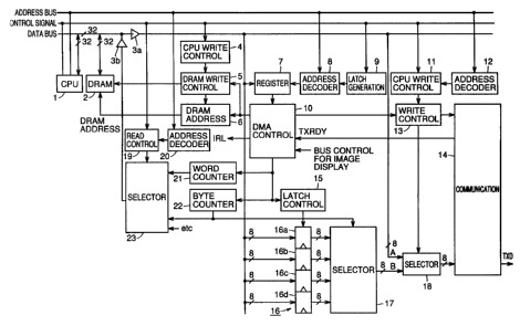
Fig. 1 is a circuit diagram of an embodiment of the present invention.
Figs. 2A to 2H are timing charts illustrating the timing of DMA
processing for transmission.
-3a-
CA 02289192 1999-11-03
Figs. 3A to 3I are timing charts illustrating the write control timing
of transmission data during DMA for transmission.
Figs. 4A to 4D are timing chants illustrating the bus control during
DMA for tr ansmission.
Best Modes for Carrying Out the Invention
For a more detailed description, the present invention will be
described according to the accompanying drawings. As seen in Fig. 1, the
data bus for a CPU 1 is formed with a width of 32 bits, and a DRAM 2, as
well as a register 7, a transmission buffer 16, and a selector 18 via an input
buffer 3a, is connected to the data bus. DRAM 2 stores image data of the
images taken by a digital still camera as transfer data. A CPU write
control circuit 4, a DMA write control circuit 5, and a DRAM address circuit
6 are provided so as to wizte control the DRAM 2.
When CPU 1 is cut off fiom the data bus, a DMA control circuit 10
performs the DMA control for reading the data stored in DRAM 2 without
involving CPU 1. CPU 1 stores a storage lead address of DRAM 2, an
address width, and a transfer start flag in register 7 via an address decoder
8, and DMA control circuit 10 reads data from DRAM 2 based on these
control data. The data read out is provided to transmission buffer 16.
Transmission buffer 16 has areas 16a to 16d, each for storing one byte of
the 4 bytes of data. Each byte of data is selected by selector 17, and
further, is written into a communication circuit 14 via selector 18 and
output to the outside.
A word counter 21 counts the number of words of the data written
into communication circuit 14, while a byi;e counter 22 similarly counts the
number of bytes. When connected with the data bus, CPU 1 can read the
count values of word counter 21 and of byte counter 22 via an output buffer
3b and a selector 23 by the control of a read control circuit 19 and an
address decoder 20.
Now, a specific operation of the embodiment shown in Fig. 1 will be
described. Communication circuit 14 is one that is compatible with 8251.
An 8251 communication circuit in its initialized state awaits the mode
-4-
CA 02289192 1999-11-03
setting. Thus, CPU 1 is required to write the mode data into
communication circuit 14. A CPU write control circuit 11 and an address
decoder 12 have addresses for communication circuitry allocated in advance,
and when CPU 1 performs the processing to write into the address
corresponding to a modelcommand of communication circuit 14, the data for
mode is written into communication circuit 14 via a write control circuit 13
and selector 18.
For asynchronous communication, for instance, the mode data sets
the start bit and the stop bit each to be 1 bit, the character length to be 8
bits, and the baud rate to be x 16 mode. When mode setting is complete,
communication circuit 14 awaits the command setting, and the command is
set by CPU 1 once again writing into the same address. Here, the
transmission enable is set to the active state.
When the transmission enable is set to the active state, the
transmission data is written into communication circuit 14 so that the
wiztten data is serially output. Moreover, when the transmission enable is
activated, a transmission ready signal (TXRD~ is activated. Further, the
transferred data has been written into DRAM 2 by CPU 1 in advance via
CPU write control circuit 4, DRAM write control circuit 5, and DRAM
address circuit 6.
Then, in this condition, setting of DMA control circuit 10 is
performed. The setting is controlled by register 7, address decoder 8, and
a latch generation circuit 9. An address is allocated for each of the several
registers controlling DMA control circuit 10, and the control data fiom CPU
1 is stored in a prescribed register. The control data, as described earlier,
include a storage lead adcliess for indicating the area of DRAM 2 that
stores the transfer data, the address width, and the transfer start flag.
When, first, the area of DRAM 2 is set and, then, the transfer start flag is
activated, one word of data is read fiom DRAM 2 as a first transfer data.
This word equals the data width of CPU 1" which in this case is 32 bits.
The data read by DMA control circuit 10 is stored temporarily in
transmission buffer 16 by the latch control. of a latch control circuit 15.
Then, the 32 bit transfer data is stored into areas 16a to 16d one byte per
-5-
CA 02289192 1999-11-03
area. Each time byte counter 22 counts up by one byte, selector 17 is
switched, and by selecting the input of selector 18 on the side of the
transmission buffer, the buffer for bits 8 to 0 is selected, and the data
therefrom is written as transmission data into communication circuit 14 by
write control circuit 13.
Figs. 2A to 2H are timing charts illustrating the timing of DMA
processing for transmission. Now, a more specific description will be given
with reference to Figs. 2A to 2H. The timing of [a] in Fig. 2A indicates
that the transmission enable of communication circuit 14 is set to the active
state with the rise of the clock signal, and that the transmission ready
signal (TXR.DY) shown in Fig. 2B is activated. After TXRDY is activated,
the transfer start flag is set to the active state at the timing indicated by
[b].
Here, it is to be understood that the setting relating to the area of DRAM 2
is alieady performed. When DMA control circuit 10 detects the transfer
start flag, an interrupt flag IRL is disabled, and DMA control circuit 10
requests CPU 1 to free the data bus at the timing of (c] as shown in Fig. 2C.
At the same time, the address of DRAM 2 is connected to the lead
address, and the respective count values of word counter 21 and byte
counter 22 shown in Figs. 2G and 2H are respectively set to 0. CPU 1
receives the bus release request, and after completing its access to the data
bus, notifies that it has freed the bus at [d] as shown in Fig. 2D. Upon
detection of the release of the bus, DMA control circuit 10 reads from
DRAM 2 the data that is set to DRAM 2 and having a one-word lead
address, while at the same time stores the data in transmission buffer 16.
When data is read from DRAM 2 at the timing of [e], the bus release
request is cancelled, and CPU 1 cancels the release of the bus at the timing
of [fj.
On the other hand, when the data inside transmission buffer 16 is
written into communication channel 14, T~R,DY becomes disabled at the
timing of [g], and the count values of word counter 21 and byte counter 22
are incremented assuming that 1 byte of data in one word has been
transmitted, while the address of DRAM 2 is incremented by DRAM
address circuit 6. At the same time, communication cixcuit 14 outputs
-6-
CA 02289192 1999-11-03
serial transmission data, and waits for another TXRDY to be provided.
When the transmission data is transmitted from communication
circuit 14, the transmission ready signal becomes active once again at the
timing of [h]. Byte counter 22 counts the not-yet-transmitted data within
the one word, selector 1? selects the data and writes the data into
communication circuit 14, and byte counter 22 alone is incremented at the
timing of [i]. Then, the transfer ready signal is disabled.
This operation is repeated until all the data of the one word is
completely transmitted, and thereafter with the acti~~ation of the
transmission ready signal, the processing from [c] to [g] is peuormed in
reading the next word data from DRAM 2.
Figs. 3A to 3I are timing charts illustrating the write control timing
of transmission data of DMA for transmission. Figs. 3A to 3I show the
timing where the transfer of the word data takes place twice. It can be
said that the above-descubed Figs. 2A to 2H are enlarged versions of the
timing shown in Figs. 3A to 3I.
The first transfer word immediately after the start of transfer
corresponds to TO as shown in Fig. 3E. This first transfer word TO is read
from DRAM 2 and stored in transmission buffer 16, and 8 lower bits are
selected. These 8 lower bits correspond t;o T00. When T00 is stored in
communication circuit 14, T00 is serially output fiom TXD of
communication circuit 14, as shown in Fig. 3G. According to the initial
setting of 8251, first, one bit is output as a start bit, and then data
corresponding to T00 is output. Finally, a stop bit is output, and the
transmission of one byte is completed.
Thereafter, the wizte transmission from the second byte (T01) to the
fourth byte (T03) to communication circuit 14 are successively repeated.
The second byte (T01) is read from DRAM 2. Similarly, the fifth byte
(T10) up to the eighth byte (T13) are processed. As shown in Figs. 3H and
3I, word counter 21 counts up by 2, and byte counter 22 counts up by 4, and
the corresponding data is written into communication circuit 14. When
TXRDY shown in Fig. 3A is activated, DNfA control circuit 10 recognizes
the termination of DMA, and notifies CPZJ 1 of the termination by
_7_
CA 02289192 1999-11-03
activating IRL as a termination interrupt signal for D1~TA. Thus, a series
of processing is completed.
When the data bus is connected to CPU 1, the respective count
values of word counter 21 and byte counter 22 are provided to CPU 1 via
selector 23 by the control of read control circuit 19 and address decoder 20
so that CPU 1 can read the respective count values. Read control circuit
19 selects the data to be read according to a read control signal of CPU 1
and an address. Moreover, an address corresponding to the data to be
read is assigned to address decoder 25. and the decode value is provided to
the read control circuit 19. Selector 23 selects the data to be read
according to a selecting signal from read control circuit 19. By reading
this value, CPU 1 is able to grasp the progress of the tr ansmission.
Further, CPU 1 can calculate the number of remaining data even when
DMA is interrupted upon receiving a request to stop transmission sent fiom
the destination of the communication.
Furthermore, it is not only DMA of the communication circuitry that
utilizes the data bus in operating the digital still camera as a system.
Occasionally, the data bus is freed from CPU 1 to allow the read from/write
into DRAM 2 in order to display an image. Since the display of an image
must involve access at determined timing or the display would be affected,
the read/write of DRAM for image display circuitry has priority.
Figs. 4A to 4D are diagrams illustrating the timing of the bus control
during DMA for transmission. In Figs. 4A to 4D, the block of image
display circuitry requests for the bus release at the timing of [a]. In
response to the request, CPU 1 terminates its access to the bus and frees
the bus at that point. If the communication circuitry shown in Fig. 4B
requests for the release of the bus at the timing of [b], the communication
circuitry monitors the bus release request. from the image display circuitry,
and since the image display circuitry is in. the process of requesting for the
bus release, the communication circuitry stands by for processing. If the
image display circuitry cancels the bus release at the timing of [c], the
communication circuitry recognizes this and starts its processing. The
processing of the communication circuitry ends at the timing of [d] and
_g_
CA 02289192 1999-11-03
when the bus release is cancelled, CPU 1 connects itself to the bus.
Thus far, in the bus control, the pexzod <a>is the processing pexzod of
the image display circuitry, the pexzod <b:> is the processing pexzod of the
communication circuitry, and the period <:c> is the period during which
CPU 1 is allowed to access the bus. Now, suppose that the communication
circuitry once again requests for the bus release at the timing of [e]. CPU
1 frees the bus in response to the request and the communication ci.rcuitxy
starts processing. At this time, the image display circuitry requests for the
bus release at the timing of [fj. The communication circuitry recognizes
this, stops the processing, and hands over the bus to the image display
circuitry. The image processing ends at t;he timing of [g], and the bus
release request is cancelled. The communication circuitry recognizes this
and resumes processing. The processing ends at the timing of [h], the bus
release request is cancelled, and CPU 1 connects itself to the bus. The bus
release request is returned to CPU 1 as ANDed signal between the image
display circuitry and the communication circuitry, and during its bus
release period, CPU 1 does not recognize which processing is being
pex~'ormed.
Industxzal Applicability
As described above, the communication DMA device accor ding to the
present invention is suitable for freeing the data bus from the CPU and
allowing image data stored in a DRAM to be output via a communication
circuit in outputting image data of an image taken by a digital still camera
to a personal computer.
-9-