Note: Descriptions are shown in the official language in which they were submitted.
CA 02289239 1999-11-10
PATENT
3535-35-17
The present invention is directed to the formation of thin layer capacitors,
preferably for
printed circuitry, such thin layers being capable of being embedded within a
printed circuit board.
In particular, the invention is directed to forming thin layer capacitors from
thin layers of
dielectric material which may be deposited by combustion chemical vapor
deposition.
Background of the Invention
Combustion chemical vapor deposition ("CCVD"), a recently invented CVD
technique,
allows for open atmosphere deposition of thin films. The CCVD process offers
several
advantages over other thin-film technologies, including traditional CVD. The
key advantage of
CCVD is its ability to deposit films in the open atmosphere without any costly
furnace, vacuum,
or reaction chamber. As a result, the initial system capitalization
requirement can be reduced up
to 90% compared to a vacuum based system. Instead of a specialized
environment, which is
required by other technologies, a combustion flame provides the necessary
environment for the
deposition of elemental constituents from solution, vapor, or gas sources. The
precursors are
generally dissolved in a solvent that also acts as the combustible fuel.
Depositions can be
performed at atmospheric pressure and temperature within an exhaust hood,
outdoors, or within a
chamber for control of the surrounding gasses or pressure.
Because CCVD generally uses solutions, a significant advantage of this
technology is that
it allows rapid and simple changes in dopants and stoichiometries which eases
deposition of
complex films. The CCVD technique generally uses inexpensive, soluble
precursors. In
addition, precursor vapor pressures in many cases does not play a role in CCVD
because the
dissolution process provides the energy for the creation of the necessary
ionic constituents. By
adjusting solution concentrations and constituents, a wide range of
stoichiometries can be
deposited quickly and easily. Additionally, the CCVD process allows both
chemical composition
1
CA 02289239 1999-11-10
PATENT
3535-35-17
and physical structure of the deposited film to be tailored to the
requirements of the specific
application.
Unlike conventional CVD, the CCVD process is not confined to an expensive,
inflexible,
low-pressure reaction chamber. Therefore, the deposition flame, or bank of
flames, can be
moved across the substrate to easily coat large and/or complex surface areas.
Because the CCVD
process is not limited to specialized environments, the user can continuously
feed materials into
the coating area without disruption, thereby permitting batch processing.
Moreover, the user can
limit deposition to specific areas of a substrate by simply controlling the
dwell time of the
flames) on those areas. Finally, the CCVD technology generally uses halogen-
free chemical
precursors having significantly reduced negative environmental impact.
Numerous materials have been deposited via CCVD technology with the combustion
of a
premixed precursor solution as the sole heat source. This inexpensive and
flexible film
deposition technique permits broad use of thin film technology. The CCVD
process has much of
the same flexibility as thermal spraying, yet creates quality, conformal films
like those associated
with conventional CVD. With CCVD processing, a desired phase can be deposited
in a few days
and at relatively low cost.
A preferred embodiment of the CCVD process is described in detail in U.S.
Application
No. 08/691,853 filed 2 August 1996, the teachings of which are incorporated
herein by
reference. In accordance with that application, the CCVD process produces
vapor formed films,
powders and nanophase coatings from near-supercritical liquids and
supercritical fluids.
Preferably, a liquid or liquid-like solution fluid containing chemical
precursors) is formed. The
solution fluid is regulated to near or above the critical pressure and is then
heated to near the
supercritical temperature just prior to being released through a restriction
or nozzle which results
in a gas entrained very finely atomized or vaporized solution fluid. The
solution fluid vapor is
combusted to form a flame or is entered into a flame or electric torch plasma,
and the
precursors) react to the desired phase in the flame or plasma or on the
substrate surface. Due to
the high temperature of the plasma much of the precursor will react prior to
the substrate surface.
2
CA 02289239 1999-11-10
v
PATENT
3535-35-17
A substrate is positioned near or in the flame or electric plasma, and a
coating is deposited.
Alternatively, the material formed can be collected as a nanophase powder.
Very fine atomization, nebulization, vaporization or gasification is achieved
using
solution fluids near or above the critical pressure and near the critical
temperature. The dissolved
chemical precursors) need not have high vapor pressure, but high vapor
pressure precursors can
work well or better than lower vapor pressure precursors. By heating the
solution fluid just prior
to or at the end of the nozzle or restriction tube (atomizing device), the
available time for
precursor chemical reaction or decomposition prior to atomization is
minimized. This method
can be used to deposit coatings from various metalorganics and inorganic
precursors. The fluid
solution solvent can be selected from any liquid or supercritical fluid in
which the precursors)
can form a solution. The liquid or fluid solvent by itself can consist of a
mixture of different
compounds.
A reduction in the supercritical temperature of the reagent containing fluid
produces
superior coatings. Many of these fluids are not stable as liquids at STP, and
must be combined in
a pressure cylinder or at a low temperature. To ease the formation of a liquid
or fluid solution
which can only exist at pressures greater than ambient, the chemical
precursors) are optionally
first dissolved in primary solvent that is stable at ambient pressure. This
solution is placed in a
pressure capable container, and then the secondary (or main) liquid or fluid
(into which the
primary solution is miscible) is added. The main liquid or fluid has a lower
supercritical
temperature, and results in a lowering of the maximum temperature needed for
the desired degree
of nebulization. By forming a high concentration primary solution, much of the
resultant lower
concentration solution is composed of secondary and possible additional
solution compounds.
Generally, the higher the ratio of a given compound in a given solution, the
more the solution
properties behave like that compound. These additional liquids and fluids are
chosen to aid in
the very fine atomization, vaporization or gasification of the chemical
precursors) containing
solution. Choosing a final solution mixture with low supercritical temperature
additionally
minimizes the occurrence of chemical precursors reacting inside the
atomization apparatus, as
CA 02289239 1999-11-10
y
PATENT
3535-35-17
well as lowering or eliminating the need to heat the solution at the release
area. In some
instances the solution may be cooled prior to the release area so that
solubility and fluid stability
are maintained. One skilled in the art of supercritical fluid solutions could
determine various
possible solution mixtures without undue experimentation. Optionally, a
pressure vessel with a
glass window, or with optical fibers and a monitor, allows visual
determination of miscibility and
solute-solvent compatibility. Conversely, if in-line filters become clogged or
precipitant is found
remaining in the main container, an incompatibility under those conditions may
have occurred.
Another advantage is that release of fluids near or above their supercritical
point results
in a rapid expansion forming a high speed gas-vapor stream. High velocity gas
streams
effectively reduce the gas diffusion boundary layer in front of the deposition
surface which, in
turn, improves film quality and deposition efficiency. When the stream
velocities are above the
flame velocity, a pilot light or other ignition means must be used to form a
steady state flame. In
some instances two or more pilots may be needed to ensure complete combustion.
Alternatively,
instead of flames, the precursor can be passed through hot gasses, plasma,
laser or other energetic
zones. With the plasma torch and other energetic zones, no pilot lights are
needed, and high
velocities can be easily achieved by following operational conditions known by
one of ordinary
skill in the art.
The solute-containing fluid need not be the fuel for the combustion.
Noncombustible
fluids like water, N20 or CO2, or difficult to combust fluids like ammonia,
can be used to
dissolve the precursors or can serve as the secondary solution compound. These
are then
expanded into a flame or plasma torch which provides the environment for the
precursors to
react. The depositions can be performed above, below or at ambient pressure.
Plasma torches
work well at reduced pressures. Flames can be stable down to 10 torr, and
operate well at high
pressures. Cool flames of even less than 500 °C can be formed at lower
pressures. While both
can operate in the open atmosphere, it can be advantageous to practice the
methods of the
invention in a reaction chamber under a controlled atmosphere to keep airborne
impurities from
being entrained into the resulting coating. Many electrical and optical
coating applications
4
CA 02289239 1999-11-10
PATENT
3535-35-17
require that no such impurities be present in the coating. These applications
normally require
thin films, but thicker films for thermal barrier, corrosion and wear
applications can also be
deposited.
Further bulk material can be grown, including single crystals, by extending
the deposition
time even further. The faster epitaxial deposition rates provided by higher
deposition
temperatures, due to higher diffusion rates, can be necessary for the
deposition of single crystal
thick films or bulk material.
CCVD is a flame process which utilizes oxygen. While it may be possible using
CCVD
to deposit oxygen-reactive materials with CCVD by depositing in the reducing
portions of the
flame, a better technique for depositing oxygen reactive materials, such as
nickel, is a related
process described in U.S. Patent Application No. 09/067,975, filed 20 April
1998, the teachings
of which are incorporated herein by reference.
The invention described in referenced U.S. Patent Application No. 09/067,975
provides an apparatus and method for chemical vapor deposition wherein the
atmosphere in a
coating deposition zone is established by carefully controlling and shielding
the materials fed to
form the coating and by causing the gases removed from the deposition zone to
pass through a
barrier zone wherein they flow away from said deposition zone at an average
velocity greater
than 50 feet per minute, and preferably greater than 100 feet per minute. The
rapid gas flow
through the barrier zone essentially precludes the migration of gases from the
ambient
atmosphere to the deposition zone where they could react with the coating or
the materials from
which the coating is derived. Careful control of the materials used to form
the coating can be
provided by feeding the coating precursors in a fixed proportion in a liquid
media. The liquid
media is atomized as it is fed to a reaction zone wherein the liquid media is
vaporized and the
coating precursors react to form reacted coating precursors. Alternatively,
the coating
precursors) can be fed as a gas, either as itself or as a mixture in a carrier
gas. The reacted
coating precursors are often composed of partially, fully and fractionally
reacted components,
which can flow as a plasma to the deposition zone. The reacted coating
precursors contact and
S
CA 02289239 1999-11-10
,~.
PATENT
3535-35-17
deposit the coating on the surface of the substrate in the deposition zone. A
curtain of flowing
inert gases may be provided around the reaction zone to shield the reactive
coating
materials/plasma in that zone from contamination with the materials used in
the surrounding
apparatus or with components of the ambient atmosphere.
The vaporization of the liquid media and reaction of the coating precursors in
the reaction
zone requires an input of energy. The required energy can be provided from
various sources,
such as electrical resistance heating, induction heating, microwave heating,
RF heating, hot
surface heating and/or mixing with hot inert gas.
Herein, non-combustion process will be referred to as "Controlled Atmosphere
Combustion Chemical Vapor Deposition" (CACCVD). This technique provides a
relatively
controlled rate of energy input, enabling high rates of coating deposition. In
some preferred
cases, the liquid media and/or a secondary gas used to atomize the liquid
media can be a
combustible fuel used in the CACCVD. Particularly important is the capability
of CACCVD to
form high quality adherent deposits at or about atmospheric pressure, thereby
avoiding the need
1 S to be conducted in elaborate vacuum or similar isolation housings. For
these reasons, in many
cases, CACCVD thin film coatings can be applied in situ, or "in the field",
where the substrate is
located.
Combustion chemical vapor deposition (CCVD) is not suitable for those coating
applications which require an oxygen free environment. For such applications,
CACCVD, which
employs non-combustion energy sources such as hot gases, heated tubes, radiant
energy,
microwave and energized photons as with infrared or laser sources are
suitable. In these
applications it is important that all of the liquids and gases used be oxygen-
free. The coating
precursors can be fed in solution or suspension in liquids such as ammonia or
propane which are
suitable for the deposit of nitrides or carbides, respectively.
CACCVD processes and apparatus provide control over the deposition zone
atmosphere,
thereby enabling the production of sensitive coatings on temperature sensitive
or vacuum
6
CA 02289239 1999-11-10
PATENT
3535-35-17
sensitive substrates, which substrates can be larger than could otherwise be
processed by
conventional vacuum chamber deposition techniques.
A further advantage of CACCVD is its ability to coat substrates without
needing
additional energy supplied to the substrate. Accordingly, this system allows
substrates to be
coated which previously could not withstand the temperatures to which
substrates were subjected
by most previous systems. For instance, nickel coatings can be provided on
polyamide sheet
substrates without causing deformation of the substrate. Previously
atmospheric pressure
deposition techniques were unable to provide chemical vapor deposition of
metallic nickel
because of its strong affinity to oxygen, while vacuum processing of polyamide
sheet substrates
was problematical due to its outgassing of water and tendency toward
dimensional instability
when subjected to heat and vacuum.
The present invention is directed particularly to the formation of thin layer
capacitors, it is
preferred that at least one layer of such capacitors being conveniently
deposited by CCVD or
CACCVD. Generally, a capacitor comprises a pair of electrically conductive
plates with a
dielectric material interposed between the plates, whereby the plates are
capable of holding an
electrical charge. Thin layer capacitors formed in accordance with the
invention involve the
formation of a thin layer of dielectric material in intimate contact with
electrically conducting
plate layers.
As a simple configuration of a thin layer capacitor, a dielectric material
layer may be
formed on a metal foil or metal layer, and a second metal layer formed on the
opposite surface of
the dielectric material layer. Such a three layer structure is itself a
capacitor and may be used, as
such, as a decoupling capacitor.
Using the three-layer structure described in the above paragraph, a plurality
of discrete
capacitors can be formed by patterning at least one of the electrically
conductive layers, typically
the second metal layer formed on the dielectric layer. Such patterning of the
metal layer can be
accomplished by conventional photoresist techniques followed by etching of the
metal layer so as
to form a pattern of discrete plates on one surface of the dielectric material
layer. In such a
7
CA 02289239 1999-11-10
PATENT
3535-35-17
structure, the other metal layer, e.g., the metal foil layer, serves as a
common capacitor plate for
holding charge relative to the opposed discrete capacitor plates.
Alternatively, both metal layers
may be patterned by photoresist/etching techniques.
Instead of the first layer being a metal foil, the first layer may also be a
thin metal layer
deposited on a polymeric film, e.g., a polyamide film. Subsequently, a
dielectric material layer
and a second metal layer are deposited thereon. The second metal layer may be
patterned as
described above to form discrete capacitor plates.
It is also possible to pattern a dielectric material layer by
photoresist/etching techniques.
For example, silica based glasses, deposited as thin dielectric material
layers in accordance with
the invention, may be etched with ammonium hydrogen difluoride, fluoroboric
acid, and
mixtures thereof.
Capacitor configurations are described, for example, in U.S. Patents Nos.
5,079,069,
5,155,655, and 5,410,107, the teachings of each of which are incorporated by
reference.
Thin layer capacitors for printed circuit boards require large areas and some
flexibility for
reasons having to do with handling, robustness, flow weight and thermal
expansion of the
materials, etc., and layered structures from which the capacitors are formed
must have some
flexibility. This is to be distinguished from the smaller more rigid
structures of silicon chip
technology. Because flexibility is required and because the dielectric
materials used herein are
generally glassy, e.g., silica, the dielectric layers are necessarily very
thin, i.e., 2 microns or
thinner, preferably 1 micron or thinner.
The substrate material should be capable of being rolled and should be
available in many
widths, and long lengths. Materials such as metals foils and polymers satisfy
these needs while
silicon does not. Silicon is easier to deposit on by most techniques because
it is stiff, does not
out-gas and is of small size. CCVD is able to coat the desired substrates with
quality coatings.
8
CA 02289239 1999-11-10
PATENT
3535-35-17
Summary of the Invention
In accordance with the present invention thin layer capacitors are formed on a
flexible
substrate, which capacitors may be embedded within a printed circuit board. On
a flexible
substrate is formed a thin layer of dielectric material. Preferably, the
dielectric material is
deposited on the substrate by combustion chemical vapor deposition (CCVD).
In one embodiment of the invention, a dielectric layer is deposited on a metal
foil, such as
copper, nickel or aluminum foil. Then, on the opposite side of the dielectric
layer is deposited a
second conducting layer, usually of metal. The second conductive layer may be
deposited
entirely by CCVD, or CACCVD. Alternatively, a seed layer, such as a thin layer
of platinum,
may be deposited by CCVD and then a thicker metal layer built up by
electroplating to form the
three-layer capacitor structure. Such a three-layer structure may, without
further processing, act
as a capacitor, e.g., a decoupling capacitor, or the three-layer structure may
be further processed
to form a mufti-capacitor component. The thin layer capacitor structures
described herein, are
typically embedded in dielectric material, e.g., epoxy-based prepreg, so as to
function as a
capacitor layer within an electronic circuit board.
Embedded capacitors of the type taught in accordance with the invention enable
further
miniaturization of printed circuit boards (PCBs) because fabrication no longer
requires discrete
capacitors that have to be large enough to be handled either by robot arms and
or humans and
soldered to the traces on the face of a printed circuit board.
Figure 1 shows a schematic diagram of the apparatus of the invention.
Figure 2 shows a schematic diagram of an apparatus for the deposition of films
and
powders using near supercritical and supercritical atomization.
Figure 3 shows a detailed schematic view of the atomizer used in the present
invention.
Figures 4A, 4B and 4C are cross-sectional views of capacitors comprising or
formed from
a three-layer structure of a metal foil, a dielectric layer, and a deposited
metal layer.
9
CA 02289239 1999-11-10
PATENT
3535-35-17
Figures SA and 5 B are cross-sectional views of a four layer capacitor
structures of a
polymeric film, a first deposited metal layer, a dielectric material layer,
and a second deposited
metal layer.
Figure 6 is a cross-sectional view of a 5-layer structure including a metal
foil, a barrier
layer, a dielectric layer, an adhesion layer and a deposited metal layer.
Figure 7 is a schematic view, partially in section, of an apparatus for
applying coatings in
accord with the present invention.
Figure 8 is a close-up perspective view, partially in section, of a portion of
the coating
head used in the apparatus of Figure 7.
The present invention may be understood more readily by reference to the
following
detailed description of preferred embodiments of the invention and the
Figures.
It is to be understood that the terminology used herein is for the purpose of
describing
particular embodiments only and is not intended to be limiting. It must be
noted that, as used in
the specification and the appended claims, the singular forms "a," "an" and
"the" include plural
referents unless the context clearly dictates otherwise.
Throughout this application, where publications are referenced, the
disclosures of these
publications in their entireties are hereby incorporated by reference into
this application in order
to more fully describe the state of the art to which this invention pertains.
The present invention provides a method for coating a substrate with a
selected material.
The method comprises, at a first selected temperature and a first selected
pressure, dissolving
into a suitable Garner to thereby form a transport solution one or more
reagents capable of
reacting (where, for a single precursor reagent, the precipitation of the
reagent from the solution
or change in chemical bonds is herein considered a "reaction") to form the
selected material. At
some time prior to the actual deposition, a substrate is positioned in a
region having a second
selected pressure. The second selected pressure can be ambient pressure and is
generally above
CA 02289239 1999-11-10
PATENT
3535-35-17
20 tort. The transport solution is then pressurized to a third selected
pressure above the second
selected pressure using a pressure regulating means. One of skill in the art
would recognize that
there are many suitable pressure regulating means, including, but not limited
to compressors, etc.
Next, the pressurized, transport solution is directed to a fluid conduit
having an input end and an
opposed output end having a temperature regulating means positioned thereon
for regulating the
temperature of the solution at the output end. The output end of the conduit
further comprises an
outlet port oriented to direct the fluid in the conduit into the region and in
the direction of the
substrate. The outlet port can be of a shape similar to a nozzle or restrictor
as used in other
spraying and atomizing applications. Thereafter, the solution is heated using
the temperature
regulating means to a second selected temperature within 50 °C above or
below the critical
temperature, T~, of the solution while maintaining the third selected pressure
above the second
selected pressure and above the corresponding liquidus or critical pressure,
P~, of the solution at
the second selected temperature using the pressure regulating means. Then, the
pressurized,
heated solution is directed through the outlet port of the conduit into the
region to produce a
nebulized solution spray in the direction of the substrate. As the solution is
directed into the
region, one or more selected gases are admixed into the nebulized solution
spray to form a
reactable spray and, thereafter, this reactable spray is exposed to an energy
source at a selected
energization point. The energy source provides sufficient energy to react the
reactable spray
(which contains the one or more reagents of the transport solutions) thereby
forming the material
and coating the substrate therewith.
In a further embodiment of this method, the energy source comprises a flame
source and
the selected energization point comprises an ignition point. In an alternate
embodiment, The
energy source comprises a plasma torch and heated gasses.
In a further embodiment of the method, the second selected pressure of the
region is
ambient pressure.
In yet another embodiment, the nebulized solution spray is a vapor or an
aerosol having a
maximum droplet size of less than 2 p,m.
11
CA 02289239 1999-11-10
PATENT
3535-35-17
In a further embodiment, the second selected pressure of the region is reduced
to produce
a combustion flame having a temperature of less than 1000 °C.
In yet another embodiment, the carrier is propane and the transport solution
comprises at
least 50 % by volume propane. In a further embodiment, the transport solution
further includes
butanol, methanol, isopropanol, toluene, or a combination thereof. In yet
another embodiment,
the Garner is selected such that the transport solution is substantially
precipitate free at standard
temperature and pressure for a period of time sufficient to carry out the
method.
In an alternate embodiment of the method, a pressurized container is used and
before,
during or after the pressuring step, a standard temperature and pressure gas
is also contacted with
the transport solution at a selected pressure sufficient to form a liquid or
supercritical fluid
(depending upon the temperature). In a preferred embodiment, the transport
solution containing
the standard temperature and pressure gas is substantially precipitate free at
the selected pressure
for a period of time sufficient to carry out the method. In yet another
embodiment, the reagent
concentration of the transport solution is between 0.0005 M and 0.05 M.
In a further embodiment, the outlet end of the conduit further comprises a
fluid
introduction port and, prior to directing the pressurized, heated solution
through the outlet port of
the conduit, fluid is added to the pressurized, heated solution through the
fluid introduction port.
Such introduction forms a combined solution having a reduced supercritical
temperature.
In yet another embodiment, each of the one or more reagents has a vapor
pressure of no
less than about 25 % of the vapor pressure of the carrier.
In a further embodiment, the outlet end of the conduit comprises tubing having
an
internal diameter of 2 to 1000 Vim, more preferably 10 to 250 Vim. In a more
preferable
embodiment, the outlet end of the conduit comprises tubing having an internal
diameter of 25 to
125 ~tm. In yet a further preferable embodiment, the outlet end of the conduit
comprises tubing
having an internal diameter of 50 to 100 ~,m.
In another embodiment, the temperature regulating means comprises means for
resistively heating the conduit by applying thereto an electric current of a
selected voltage from
12
CA 02289239 1999-11-10
PATENT
3535-35-17
an electric current source. In a preferred embodiment, the voltage is less
than 115 Volts. In yet
another preferred embodiment, the means for resistively heating the conduit
comprises a contact
positioned within 4 mm of the outlet port.
Moreover, the present invention also provides the above method wherein the
Garner and
S one or more reagents are selected such that the second selected temperature
is ambient
temperature.
The above method may be practiced wherein the material that coats the
substrate
comprises a metal, a metal or metalloid oxide, or a mixture of a metal with a
metal or metalloid
oxide.
In a further embodiment, the reactable spray comprises a combustible spray
having a
combustible spray velocity and wherein the combustible spray velocity is
greater than the flame
speed of the flame source at the ignition point and further comprising one or
more ignition
assistance means for igniting the combustible spray. In a preferred
embodiment, each of the one
or more ignition assistance means comprises a pilot light. In yet another
embodiment, the
combustible spray velocity is greater than mach one.
In a further embodiment, the ignition point or flame front is maintained
within 2 cm. of
the outlet port.
The present invention also provides a method where, during the exposing step,
the
substrate is cooled using a substrate cooling means. In a preferred
embodiment, the substrate
cooling means comprises a means for directing water onto the substrate.
However, one of
ordinary skill in the art would recognize that many other suitable cooling
means could be used.
In a further embodiment, the material that coats the substrate has a thickness
of less than
500 run. In yet another embodiment, the material that coats the substrate
comprises a graded
composition. In another embodiment, the material that coats the substrate
comprises an
amorphous material. In a further embodiment, the material that coats the
substrate comprises a
nitride, carbide, boride, metal or other non-oxygen containing material.
13
CA 02289239 1999-11-10
PATENT
3535-35-17
The present invention also provides a method further comprising flowing a
selected
sheath gas around the reactable spray thereby decreasing entrained impurities
and maintaining a
favorable deposition environment.
In a preferred embodiment, the second selected pressure is above 20 torr.
Referring now to Figure 1, the preferred apparatus 100 comprises a pressure
regulating
means 110, such as a pump, for pressurizing to a first selected pressure a
transport solution T
(also called "precursor solution") in a transport solution reservoir 112,
wherein the transport
solution T comprises a suitable carrier having dissolved therein one or more
reagents capable of
reacting to form the selected material and wherein the means for pressurizing
110 is capable of
maintaining the first selected pressure above the corresponding liquidus (if
the temperature is
below T~) or critical pressure, P~,, of the transport solution T at the
temperature of the transport
solution T, a fluid conduit 120 having an input end 122 in fluid connection
with the transport
solution reservoir 112 and an opposed output end 124 having an outlet port 126
oriented to direct
the fluid in the conduit 120 into a region 130 of a second selected pressure
below the first
selected pressure and in the direction of the substrate 140, wherein the
outlet port 126 further
comprises means 128 (see Figures 2 and 3, atomizer 4) for nebulizing a
solution to form a
nebulized solution spray N, a temperature regulating means 150 positioned in
thermal connection
with the output end 124 of the fluid conduit 120 for regulating the
temperature of the solution at
the output end 124 within 50 °C above or below the supercritical
temperature, T~, of the solution,
a gas supply means 160 for admixing one or more gases (e.g., oxygen) (not
shown) into the
nebulized solution spray N to form a reactable spray, an energy source 170 at
a selected
energization point 172 for reacting the reactable spray whereby the energy
source 170 provides
sufficient energy to react the reactable spray in the region 130 of the second
selected pressure
thereby coating the substrate 140.
In a further embodiment of the apparatus, the energy source 170 comprises a
flame source
and the selected energization point 172 comprises an ignition point. In an
alternate embodiment,
14
CA 02289239 1999-11-10
PATENT
3535-35-17
the energy source 170 comprises a plasma torch. In yet another embodiment, the
outlet port 126
further comprises a pressure restriction (see Figure 3, restrictor 7).
In a further embodiment of the apparatus, the second selected pressure of the
region is
ambient pressure.
In yet another embodiment, the nebulized solution spray N is a vapor or an
aerosol having
a maximum droplet size of less than 2 Vim.
In a further embodiment, the second selected pressure of the region is reduced
to produce
a combustion flame having a temperature of less than 1000 °C.
In yet another embodiment, the carrier is propane and the transport solution
comprises at
least 50 % by volume propane. In a further embodiment, the transport solution
further includes
butanol, methanol, isopropanol, toluene, or a combination thereof. In yet
another embodiment,
the carrier is selected such that the transport solution is substantially
precipitate free at standard
temperature and pressure for a period of time sufficient to carry out the
method.
In an alternate embodiment of the apparatus, a pressurized container (not
shown) is
provided and a standard temperature and pressure gas is also contacted with
the transport
solution at a selected pressure sufficient to form a liquid or supercritical
fluid. In a preferred
embodiment, the transport solution containing the standard temperature and
pressure gas is
substantially precipitate free at the selected pressure for a period of time
sufficient to carry out
the method. In yet another embodiment, the reagent concentration of the
transport solution is
between 0.0005 M and 0.05 M.
In a further embodiment, the outlet end 124 of the conduit 120 further
comprises a fluid
introduction port (see Figure 2, feed lines 17 or 19) and, prior to directing
the pressurized, heated
solution through the outlet port 126 of the conduit 120, fluid is added to the
pressurized, heated
solution through the fluid introduction port. Such introduction forms a
combined solution having
a reduced supercritical temperature.
In yet another embodiment, each of the one or more reagents has a vapor
pressure of no
less than about 25 % of the vapor pressure of the carrier.
CA 02289239 1999-11-10
PATENT
3535-35-17
In a further embodiment, the outlet end of the conduit comprises tubing having
an
internal diameter of 2 to 1000 Vim, more preferably 10 to 250 Vim. In a more
preferable
embodiment, the outlet end of the conduit comprises tubing having an internal
diameter of 25 to
125 Vim. In yet a further preferable embodiment, the outlet end of the conduit
comprises tubing
S having an internal diameter of 50 to 100 ~tm.
In another embodiment, the temperature regulating means 150 comprises means
for
resistively heating the conduit by applying thereto an electric current of a
selected voltage from
an electric current source. In a preferred embodiment, the voltage is less
than 115 Volts. In yet
another preferred embodiment, the means for resistively heating the conduit
comprises a contact
152 positioned within 4 mm of the outlet port 126.
Moreover, it is provided that the above apparatus is utilized wherein the
carrier and one
or more reagents are selected such that the second selected temperature is
ambient temperature.
The above apparatus may be used wherein the material that coats the substrate
140
comprises a metal. Alternatively, the material that coats the substrate 140
comprises one or more
metal oxides. In yet a further embodiment, the material that coats the
substrate 140 comprises at
least 90 % silica.
In a fiuther embodiment, the reactable spray comprises a combustible spray
having a
combustible spray velocity and wherein the combustible spray velocity is
greater than the flame
speed of the flame source at the ignition point 172 and further comprising one
or more ignition
assistance means 180 for igniting the combustible spray. In a preferred
embodiment, each of the
one or more ignition assistance means 180 comprises a pilot light. In yet
another embodiment,
the combustible spray velocity is greater than mach one.
In a further embodiment, the ignition point 172 or flame front is maintained
within 2 cm.
of the outlet port.
The present invention also provides a substrate cooling means 190 for cooling
the
substrate 140. In a preferred embodiment, the substrate cooling means 190
comprises a means
16
CA 02289239 1999-11-10
PATENT
3535-35-17
for directing water onto the substrate 140. However, one of ordinary skill in
the art would
recognize that many other suitable cooling means could be used.
In a further embodiment, the material that coats the substrate 140 has a
thickness of less
than 500 nm. In yet another embodiment, the material that coats the substrate
140 comprises a
graded composition.
There is further an apparatus provided comprising a means (see Figures 2 and
3, feed line
17 or 19) for flowing a selected sheath gas around the reactable spray thereby
decreasing
entrained impurities and maintaining a favorable deposition environment.
In a preferred embodiment, the second selected pressure is above 20 torn.
In a further embodiment of the method, the energy source comprises a flame
source and
the selected energization point comprises an ignition point. In an alternate
embodiment, the
energy source comprises a plasma torch, hot gasses, etc.
In a further preferred embodiment of the powder forming method, the transport
solution
concentration is between 0.005 M and 5 M.
To simplify the operation, it is helpful to pump the precursor/solvent
solution to the
atomizing device at room temperature. Heating of the solution should occur as
a final step just
prior to release of the solution into the lower pressure region. Such late
stage heating minimizes
reactions and immiscibilities which occur at higher temperatures. Keeping the
solution below
the supercritical temperature until atomization maintains the dissolved
amounts of precursor in
the region of normal solubility and reduces the potential of developing
significant solvent-
precursor concentration gradients in the solution. These solubility gradients
are a result of the
sensitivity of the solution strength of a supercritical solvent with pressure.
Small pressure
gradients (as they can develop along the precursor-solvent system delivery)
can lead to
significant changes in solubility as has been observed. For instance, the
solubility of acridine in
carbon dioxide at 308 °K can be increased 1000 times by increasing the
pressure from 75 atm to
85 atm. See V. Krukonis, "Supercritical Fluid Nucleation of Difficult to
Comminute Solids",
Presented at AIChE Meeting, San Francisco, November 25-30, 1984. Such
solubility changes
17
CA 02289239 1999-11-10
w
PATENT
3535-35-17
are potentially detrimental because they may cause the precursor to be driven
out of solution and
precipitate or react prematurely, clogging lines and filters.
The rapid drop in pressure and the high velocity at the nozzle cause the
solution to
expand and atomize. For solute concentrations in the normal solubility range,
preferred for
operation of the near supercritical atomization system of the present
invention, the precursors are
effectively still in solution after being injected into the low pressure
region. The term
"effectively in solution" must be understood in conjunction with processes
taking place when a
solution with solute concentrations above the normal solvent strength is
injected into the low
pressure region. In this case, the sudden pressure drop causes high
supersaturation ratios
responsible for catastrophic solute nucleation conditions. If the catastrophic
nucleation rapidly
depletes the solvent from all dissolved precursor, the proliferation of small
precursor particles is
enhanced. See D.W. Matson, J.L. Fulton, R.C. Petersen and R.D. Smith, "Rapid
Expansion of
Supercritical Fluid Solutions: Solute Formation of Powders, Thin Films, and
Fibers", Ind. Eng.
Chem. Res., 26, 2298 (1987); H. Anderson, T.T. Kodas and D.M. Smith, "Vapor
Phase
1 S Processing of Powders: Plasma Synthesis and Aerosol Decomposition", Am.
Ceram. Soc. Bull.,
68, 996 (1989); C.J Chang and A.D Randolph, " Precipitation of Microsize
Organic Particles
from Supercritical Fluids", AIChE Journal, 35, 1876 (1989); T.T. Kodas,
"Generation of
Complex Metal Oxides by aerosol Processes: Superconducting Ceramic Particles
and Films",
Adv. Mater., 6, 180 (1989); E. Matijevic, " Fine Particles: Science ad
Technology", MRS
Bulletin, 14, 18 (1989); E. Matijevic, " Fine Particles Part II: Formation
Mechanisms and
Applications", MRS Bulletin,15, 16 (1990); R.S. Mohamed, D.S. Haverson, P.G.
Debenedetti
and R.K. Prud'homme, " Solid Formation After Expansion of Supercritical
Mixtures," in
Supercritical Fluid Science and Technology, edited by K.P. Johnston and J.M.L.
Penniger, p.355,
American Chemical Society, Washington, DC (1989); R.S. Mohamed, P.G.
Debenedetti and
R.K. Prud'homme, "Effects of Process Conditions on Crystals Obtained from
Supercritical
Mixtures", AIChE J., 35, 325 (1989); J.W. Tom and P.G. Debenedetti, "Formation
of
Bioerodible Polymeric Microspheres and Microparticles by Rapid Expansion of
Supercritical
18
CA 02289239 1999-11-10
PATENT
3535-35-17
Solutions", Biotechnol. Prog., 7, 403 (1991). Particles are undesirable for
the formation of thin
coatings, but can be beneficial do=ing the formation of powders.
Thus the heated atomizer provides the further superior advantages, compared to
an
unheated device that operates on rapid expansion of a solvent at exclusively
above the
supercritical temperature, that ( 1 ) the temperature allows for a well
controlled degree of
atomization of the precursor-solvent mixture and (2) catastrophic nucleation
of the precursors
can be omitted while still enjoying the benefits of supercritical atomization.
Supersonic
velocities can be created forming a mach disk which additionally benefits
atomization. Addition
of gasses to the released atomized materials aids in directing the flow and
can ensure a desired
mixture for combustion.
By adjusting the heat input into the atomizing device, the liquid solution can
be vaporized
to various degrees. With no heat input to the atomizing device, liquid
solutions of higher
supercritical temperature liquids, that are liquids at STP, can exit in the
form of a liquid stream
which is clearly far from a supercritical condition. This results in a poorly
formed flame and,
possibly, undesirable liquid contact with the substrate. Decreasing the
temperature differential of
the liquid solution to its supercritical temperature at the nozzle causes the
liquid solution to break
up into droplets forming a mist which is released from the atomizing device.
The droplets
vaporize, and thus become invisible, after a short distance. As the
supercritical temperature at
the atomizing device is approached, the liquid solution droplets decrease in
size, and the distance
to solution vaporization is decreased. Using this atomizer the vapor droplet
size was determined
using an laser aerosol particle size tester and the obtained droplet size was
below the 1.8 ~.m
detection limit of the instrument.
Further increasing the heat input results in a state of no mist at the tip, or
complete
vaporization. Without wishing to be bound by theory, this behavior of the
solution can be
attributed to the combined supercritical properties of the reagents and
solvents. Solutions of
precursors in lower supercritical temperature solvents, that are gasses at
STP, behave similarly,
but the emerging solution from the tip (also referred to as the "nozzle" or
"restrictor") does not
19
CA 02289239 1999-11-10
PATENT
3535-35-17
form a liquid stream, even without heat input. The amount of heat needed to
obtain optimal
vaporization of the solution depends mostly on the heat capacity of the
solution and the
differential between the supercritical temperature of the solvent and the
ambient temperature
around the nozzle.
It is desirable to maintain the pressure and temperature of the system (before
vaporization) above the boiling and the supercritical point of the solution.
If the pressure falls
below the liquidus or critical pressure, coincident with the temperature above
the boiling point,
vaporization of the solvents will occur in the tube prior to the tip. This
leaves the solutes which
can build up and clog the atomizing device. Similarly the pressure is
preferably sufficiently high
in the supercritical region so that the fluid is more liquid-like. Liquid-like
supercritical fluids are
better solvents than more gas-like supercritical fluids, further reducing the
probability of solutes
clogging the atomizing device. If the precursor-to-precursor interaction is
higher than the
strength between solvent and precursor, the solvent-precursor interactions can
be broken and
effectively drive the precursor out of solution. Precursor molecules then form
clusters that
adhere to the atomizing device and clog the restrictor. The problem can be
solved, in most cases,
by shifting the vaporization point from the inside of the tip to the end of
the tip, which is
accomplished by reducing the heat input into the atomizing device. Another
solution is to use a
solvent which interacts more strongly with the precursor so a more stable
solution is formed. A
small amount of mist at the tip usually results in the best quality thin
films. Nano- or micro-
spheres of the material will form if the temperature of the solution it too
high or too low. These
spheres are detrimental if dense coatings are desired.
If the no-mist condition is reached, the deposition is being performed above
the critical
temperature. The heat of the flame and mixing with external gasses keeps STP
liquid solvents
from condensing and forming droplets. In the no-mist instance, atomization and
intermixing is
very good but flow stability is reduced, resulting in a flame that can jump
from side to side with
respect to the direction of the tip. With such a flame behavior, depositions
remain possible, but it
can be difficult to deposit films requiring stringent thickness uniformity.
Additionally, it is
CA 02289239 1999-11-10
PATENT
3535-35-17
necessary to maintain the temperature of the solution, prior to release, below
the temperature
where either the solute precipitates or reacts and precipitates. When using a
solvent mixture it
may be possible during heating to cross the line for spinoidal immiscibility.
This causes the
formation of two separate phases, with the possibility of concentration
differences in the two
phases due to different solubilities of the solutes. This may influence the
formation of precursor
and product spheres at high atomization temperatures. All of these factors
demonstrate the
preferability of minimizing the solution's exposure to heating, if necessary,
until the tip so that
possible unwanted equilibrium condition states of matter do not have
sufficient time to transpire.
The structure of the films deposited can thus be precisely controlled.
Due to this control, a number of film microstructures are possible. By
increasing solution
concentration it is possible to increase the deposition rate and the following
microstructural
changes result with increasing solution concentration; dense to porous,
specular to dull, smooth
to rough, columnar to hillocks, and thin to thick. Graded and multilayered
coatings can also be
produced. Multilayers can be formed by supplying different precursor
containing solutions to an
individual flame. Sequential multiple deposition flames may be used to
increase throughput for
production applications. Some additional factors controlling deposition
parameters include;
substrate surface temperature which controls surface diffusion and nucleation;
pressure which
controls boundary layer thickness and thus deposition rate, solution
composition and mix gasses
varies the material being deposited and thus the coatings growth habit, flame
and plasma energy
level effects where the reaction occurs and vapor stability, and the distance
to the substrate
effects the time from nebulization to reaction to deposition which can lead to
particle formation
or increased diffusion time for larger clusters. Additionally, electric and
magnetic fields affect
the growth habits of some materials, or increase deposition efficiency. One of
ordinary skill in
the art would recognize that such electric and magnetic fields will affect the
growth habits of
some vapor deposited materials, as well as vary the particular deposition rate
and efficiency.
Because the required energy input into the solution heating atomizer varies
for different
precursor/primary-solvent/secondary-solvent solutions, it is preferred to
deposit multilayer thin
21
CA 02289239 1999-11-10
PATENT
3535-35-17
films from solutions with constant primary to secondary solvent ratios. In so
doing, it is not
necessary to change the energy input to the atomizer when switching from one
solution to
another solution. The resulting simplification of the setup produces increased
performance and
reliability while reducing costs. Alternatively, the substrate can be passed
by flames containing
different reagents to build the desired multilayer.
When the solution provides the fuel for combustion, concentrations up to 0.1
molar result
in dense coatings depending on the material. Most materials have preferred
concentrations of up
to 0.01 molar. Materials with lower diffusion and mobility need solution
concentrations of less
than 0.002. Solution concentrations of less than 0.0001 molar result in very
slow deposition rates
for most materials. Flame depositions with added combustible materials can
have higher
concentrations, even exceeding 1 M, but for the preferable vapor formation of
the precursors,
high concentrations are less desirable unless the precursors) have high vapor
pressures. Low
vapor pressure precursor solution concentrations are preferably less than
0.002 molar.
Without wishing to be bound by theory, it is helpful to understand that the
principle of the
deposition technique of the present invention involves the finding that CVD
its not limited to
reactions at the surface. See Hunt, A.T., "Combustion Chemical Vapor
Deposition, a Novel Thin
Film Deposition Technique", Ph.D. Thesis Georgia Inst. of Tech, Atlanta, GA.,
(1993); Hunt,
A.T., "Presubstrate Reaction CVD, and a Definition for Vapor", presented at
the 13th Int. Conf.
on CVD, Los Angles, CA (1996), the contents of which are hereby incorporated
by this
reference. Reactions can occur predominately in the gas stream, but the
resulting material which
is deposited must be subcritical in size to yield a coating with vapor
deposited microstructures.
These observations demonstrate that a vapor is composed of individual atoms,
molecules or
nanoclusters which can be absorbed onto a substrate and readily diffused into
lower energy sites
or configurations. Thus the maximum cluster size must decrease with lower
substrate
temperatures as does the critical nucleus size. It is known by one of ordinary
skill in the art that
reagent clusters are left after vaporization of the solvents, and the cluster
size is related to the
reagent vapor pressure, initial droplet size and the solution concentration.
Therefore, atomization
22
CA 02289239 1999-11-10
PATENT
3535-35-17
of low vapor pressure reagents, which therefore do not gasify in the flame,
must be very fine to
form vapor.
Preferred liquid solvents are low cost solvents and include, but are not
limited to, ethanol,
methanol, water, isopropanol and toluene. Water solutions must be fed into a
preexisting flame,
while the combustible solvents can themselves be used to form the flame. It is
preferable, but
not required, to form the bulk of the flame using the solution rather than
feeding the solution into
a flame. Lower reagent concentration results this way, which eases the
formation of subcritical
nucleus sized materials.
One preferred solvent and secondary solution fluid which is propane, which is
a gas at
STP. However, it must be noted that many other solvent systems are operable.
See, e.g., ~
Handbook of Chemistry and Ph,~, CRC Press, Boca Raton, Florida. Propane is
preferred
because of its low cost, its commercial availability, and its safety. Many low
cost organometallic
precursors can be used in a predominately propane solution. To ease handling,
the initial
precursors can be dissolved in methanol, isopropanol, toluene or other
solvents compatible with
propane. This initial solution is then placed into a container into which
liquid propane is added.
Propane is a liquid at above only about 100 psi at room temperatures. The
resulting solution has
a much lower supercritical point than the initial solution which eases
atomization by lowering the
required energy input into the atomizer. Additionally, the primary solvent
acts to increase the
polar solubility of the propane, thus allowing higher solution concentrations
for many reagents
than would otherwise be achieved by propane alone. As a general rule, the
polarity of the
primary solvent should increase with increasing polarity of the solute
(precursor). Isopropanol
can thus aid in the solubility of a polar solute better than toluene. In some
cases the primary
solvent acts as a stableizer between the secondary solvent and a ligand on the
solute. One
example is the dissolution of platinum (II) acetylacetonate
[Pt(CH3COCHCOCH3)Z] in propane,
where a polar primary solvent is required to achieve solubility in propane.
The degree of
solubility of platinum (II) acetylacetonate is very sensitive to the weight
ratios of the precursor to
the primary solvent, and of the primary solvent to the secondary solvent. The
optimum ratio of
23
CA 02289239 1999-11-10
PATENT
3535-35-17
the primary solvent to the secondary solvent is higher for platinum (II)
acetylacetonate than is
typically used with other organometallic precursors. One of ordinary skill in
the act could readily
determine the optimum ratios through experimentation.
Ammonia has been considered and tested as a secondary solvent for the
deposition of
coatings and powders. While ammonia is an inexpensive solvent that is
compatible with some
nitrate based precursors, it is not easily usable with other secondary
solvents and problems stem
from the general aggressiveness of pure ammonia. The atomization properties of
ammonia were
tested without the addition of a precursor and the used pressure vessel was
significantly attacked
after the experiment even when an inert Type-316 stainless steel vessel was
used. In contrast to
hydrocarbon based solvents, ammonia also renders Buna-N and Viton gaskets
useless after only a
few minutes. Even with a suitable gasket material this is a problem since the
desired coatings or
powders usually must not contain traces of iron or other elements leached from
the pressure
vessel wall. However, there are materials, such as EPDM elastomer which may be
used. Ni has
been deposited from a ammonia-water mix with Ni-amine-nitrate formed
precursor.
Other gas-like secondary solvents that were tested and can be used include
ethane,
ethylene, ethane/ethylene mixture, propane/ethylene mixture, and
propane/ethane mixture.
Platinum thin films were deposited from a supercritical mixture of ethane and
a platinum
metalorganic.
Other tested solvents and solvent mixtures resulted in similar quality, but
were more
complex to work with since their boiling points are significantly lower, which
required cooling of
the solution or very high pressures. The ease of handling makes propane the
preferred solvent
but the other supercritical solvents are considered alternatives to propane in
cases where propane
cannot be used, such as when a precursor that is soluble in propane cannot be
found. Other fluids
can be used to further reduce the supercritical temperature if desired.
One heating method is the application of an electric current between the
nozzle end,
where the precursor solution is injected into the low pressure region, and the
back of the
restriction tube. This directly heated restrictive tube method allows for fast
changes in
24
CA 02289239 1999-11-10
PATENT
3535-35-17
atomization due to a short response time. The location of most intense heating
can be shifted
toward the tip by increasing the connection resistance between the tip and the
electrical lead
connected to the tip. Thin walled restriction tubes possess a larger
resistance than thick walled
tubes and decrease the response time. Other heating methods can be applied and
several have
been investigated, including but not limited to, remote resistive heating,
pilot flame heating,
inductive heating and laser heating. One of ordinary skill in the art could
readily determine other
suitable heating means for regulating the temperature at the outlet port of
the atomizer.
Remote resistive heating uses a non-conducting restriction tube that is
located inside an
electrically heated tube. The non-conducting tube will fit tightly into the
conductive tube.
Application of an electric current to the conductive type heats that tube and
energy is transferred
into the inner, non-conductive restriction tube. This method requires larger
heating currents
compared to the directly-heated restrictive tube method and shows longer
response times, which
can be advantageous under certain conditions since the increased response time
results in a high
degree of thermal stability. On the other hand, pilot flame and laser heating
use the energy of the
pilot flame or laser light, respectively, to heat the restriction tube. This
can be done in a directly
heated setup where the tip of the restriction tube is subjected to the pilot
flame or laser light or in
an indirectly heated configuration where the larger outer tube is heated.
Because the amount of
energy that needs to be transferred into the solution is quite large, the
heated tube will,
preferably, have a thicker wall than in the case of direct electrical heating
or remote electrical
heating. Subjecting an outer tube to the pilot flame or laser light allows the
use of a thin walled
restriction tube.
Referring now to Figures 2 and 3, an apparatus 200 for the deposition of films
and
powders using supercritical atomization is shown. The apparatus 200 consists
of a fixed or
variable speed pump 1 that pumps the reagent transport solution 2 (also called
"precursor
solution") from the solution container 3 into the atomizer (also referred to
as the "nebulizer" or
"vaporizer") 4. Figure 3 is an inset view showing a more detailed schematic
view of the atomizer
4. The precursor solution 2 is pumped from the precursor solution container 3
through lines 5
CA 02289239 1999-11-10
PATENT
3535-35-17
and filters 6 and into the atomizer 4. The precursor solution 2 is then pumped
into a constant or
variable temperature controlled restrictor 7. Heating can be accomplished in
many ways
including, but not limited to, resistive electrical heating, laser heating,
inductive heating, or flame
heating. For resistive electrical heating, either AC or DC current can be
used. One of the
electrical connections 8 to the restrictor 7 is preferably placed very close
to the tip of the
restrictor 7. In the case of heating by a DC source, this connection 8 or pole
can be either
positive or negative. The other pole 9 can be connected at any other point
along the restrictor 7,
inside or outside the housing 10. For special applications such as coating the
inside of tubes,
where a small total atomizer size is advantageous, it is preferable to either
connect to the
restrictor 7 at the back of the housing 10 or to connect inside the housing
10. Gas connections at
the back of the housing 10 are shown in an on-line arrangement but can be
placed in any other
arrangement that does not interfere with the function of the apparatus 200.
The thin gas A supply line 11, 1/16 " ID in most cases, carries a combustible
gas mix to a
small outlet 12 where it can serve as a stable pilot flame, preferably within
2.5 cm of the
restrictor 7, for the combustion of the precursor solutions supplied via the
restrictor 7. Gas A
supply is monitored by a flow controller 13, controlling the flow of the
individual gas A mix
components,14 and 15. The gas A fuel component 14 is mixed with the oxidizing
component 15
in a mixing "T" 16 close to or inside the atomizer 4. This late mixing is
preferably for safety
reasons because it reduces potential flash-back. Distribution channels inside
the housing 10
connect the gas supply lines 11 to the gas A feed 17. Gas B supply lines 18
are used to deliver
gas B from the supply 19 such that good mixing with the nebulized solutions
spray can be
accomplished. In most cases a high velocity gas stream is utilized. A number
of gas B supply
holes 20 (six for most cases, more or less holes can be used depending on the
particular
application) is placed around the restrictor 7 supplying gas B such that the
desired flow pattern is
obtained. The flow properties of the gas B stream are influenced by such
factors as gas B
pressure in the gas B storage container 21, flow rate as determined by the
flow controller 13, line
diameters 5, and number of supply holes 20. Alternatively, gas B can be fed
through a larger
26
CA 02289239 1999-11-10
PATENT
3535-35-17
tube coaxial to and surrounding the restrictor 7. Once the precursor solution
2 has been pumped
into the precursor supply 22 its temperature is controlled by the current flow
(in the case of
electrical heating) through the restrictor 7 as determined by the power supply
23. This heating
current can then be adjusted such that the proper amount of atomization
(nebulization,
vaporization) can occur. The stable pilot flame is then capable of igniting
the nebulized reactive
spray and depositing a powder or film on a substrate 24.
Many different coatings have been deposited using the methods and apparatuses
described herein. While propane was used in most cases as the supercritical
secondary solvent
(i.e. a small amount of high precursor concentration primary solvent was mixed
with a large
amount of secondary solvent), others solvents have been used. Other possible
secondary solvents
include, but are not limited to NZO, ethylene, ethane, and ammonia.
One of ordinary skill in the art would recognize that almost any substrate can
be coated
by the method and apparatus of the present invention. A substrate can be
coated if it can
withstand the temperature and conditions of the resulting hot gases produced
during the process.
Substrates can be cooled using a means for cooling (described elsewhere
herein), such as a water
jet, but at low substrate surface temperatures, dense or crystalline coatings
of many materials are
not possible because of the associated low diffusion rates. In addition,
substrate stability in the
hot gases can be further accounted for by using a low temperature, low
pressure flame, either
with or without additional substrate cooling.
A variety of chemical precursors have been suggested for CCVD deposition of
films
and powders, and additional chemical precursors are suggested herein. In
addition to
providing the metal or metalloid element, it is required of any chemical
precursor for CCVD
that it be soluble in a suitable carrier solvent, most desirably soluble in
propane. Furthermore,
if the precursor solution is to contain precursors of more than one metal
and/or metalloid, the
chemical precursors must be mutually soluble in a suitable carrier solvent and
chemically
compatible with each other. If a precursor is not highly soluble in a primary
solvent, such as
propane, it may be initially dissolved in a secondary solvent, such as
toluene, and subsequently
27
CA 02289239 1999-11-10
PATENT
3535-35-17
introduced into the primary solvent as a solution in the secondary solvent,
providing that the
chemical precursor does not precipitate when such a solution is introduced
into the primary
solvent. Furthermore, cost considerations enter into the choice of chemical
precursor.
If a mixture of chemical precursors are to be provided for depositing a layer
or powder
of a particular composition, it is desirable that such precursors be
combinable as a
homogeneous "pre-solution" without the addition of any additional solvent. If
not, it is
desirable that all chemical precursors be mutually soluble in a common
solvent, the less solvent
the better, as a "pre-solution" . These desired properties, of course,
facilitate shipping and
handling, particularly when the intended primary solvent is propane or another
material which
is gaseous at room temperature. Though desirable to be able to provide a "pre-
solution", it is
considered acceptable that the chemical precursors be mutually soluble in a
deposition solution
of one or more solvents and either be prepared and sold as such a solution or
prepared on-site
as a deposition solution.
For deposition, the total concentration of the precursor compounds in the
carrier
solvent is generally between about 0.001 and about 2.5 wt % , preferably
between about 0.05
and about 1.0 wt % .
For most CCVD depositions, it is preferred that the precursors be dissolved in
an
organic solvent. However, for the capacitor materials to which the present
invention is
directed, it is undesirable that carbon co-deposits with the dielectric
material. Next to the
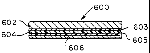
dielectric is the 2nd electrode. Some conductive materials, nickel, for
example, have a high
affinity for carbon. Accordingly, precursors for such materials may be
preferably dissolved in
an aqueous and/or ammonia solution, in which case, the aqueous and/or ammonia
and/or NZO
solution would be aspirated into a hydrogen/oxygen flame for CCVD.
One of the advantages of CCVD, as performed with preferred atomizing
apparatus,
relative to other deposition methods, is that the a precursor solution
containing one or more
dissolved chemical precursors is atomized as a near-super critical liquid or,
in some cases, as a
super critical fluid. Accordingly, the amount of precursor or precursors being
burned and
28
CA 02289239 1999-11-10
PATENT
3535-35-17
deposited on a substrate or deposited in powder form is independent of the
relative vapor
pressures of the individual chemical precursors and the carrier solvent or
solvents. This is in
contrast to conventional CVD processes where individual supply lines must be
provided for
each chemical precursor that is to be vaporized, generally within a carrier
gas, for supply to a
CVD furnace. Also, some conventional CVD precursors disproportionate, making
it difFcult
to supply such a chemical precursor uniformly--another problem readily
addressed by CCVD
technology.
A Controlled Atmosphere Combustion Chemical Vapor Deposition (CACCVD)
apparatus is illustrated in Figures 7 and 8. A coating precursor 710 is mixed
with a liquid media
712 in a forming zone 714, comprising a mixing or holding tank 716. The
precursor 710 and
liquid media 712 are formed into a flowing stream which is pressurized by pump
718, filtered by
filter 720 and fed through conduit 722 to an atomization zone 724, from which
it flows
successively through reaction zone 726, deposition zone 728 and barrier zone
730. It is not
required that a true solution be formed from mixing the coating precursor 710
with the liquid
media 712, provided the coating precursor is sufficiently finely divided in
the liquid media.
However, the formation of a solution is preferred, since, generally, such
produces a more
homogeneous coating.
The flowing stream is atomized as it passes into the atomization zone 724.
Atomization
can be accomplished by recognized techniques for atomizing a flowing liquid
stream. In the
illustrated apparatus, atomization is effected by discharging a high velocity
atomizing gas stream
surrounding and directly adjacent the flowing stream as it discharges from
conduit 722. The
atomizing gas stream is provided from a gas cylinder or other source of high
pressure gas. In the
illustrated embodiment, high pressure hydrogen (HZ) is used both as an
atomizing gas and as a
fuel. The atomizing gas is fed from hydrogen gas cylinder 732, through
regulating valve 734,
flowmeter 736 and into conduit 738. Conduit 738 extends concentrically with
conduit 722 to the
atomization zone where both conduits end allowing the high-velocity hydrogen
atomizing gas to
contact the flowing liquid stream thereby causing it to atomize into a stream
of fine particles
29
CA 02289239 1999-11-10
PATENT
3535-35-17
suspended in the surrounding gas/vapors. This stream flows into the reaction
zone 726 wherein
the liquid media vaporizes and the coating precursor reacts to form a reacted
coating precursor,
which often involves dissociation of the coating precursor into ions of its
components and results
in a flowing stream of ionic particles, or plasma. The flowing stream/plasma,
passes to the
deposition zone 728 wherein the reacted coating precursor contacts the
substrate 740 depositing
the coating thereon.
The flowing stream may be atomized by injecting the atomizing gas stream
directly at the
stream of liquid media/coating precursor as it exits conduit 722.
Alternatively, atomization can
be accomplished by directing ultrasonic or similar energy at the liquid stream
as it exits conduit
722.
The vaporization of the liquid media and reaction of the coating precursor
require
substantial energy input to the flowing stream before it leaves the reaction
zone. This energy
input can occur as it passes through the conduit 722, or in the atomization
and/or reaction zones.
The energy input can be accomplished by a variety of known heating techniques,
such as
electrical resistance heating, microwave or RF heating, electrical induction
heating, radiant
heating, mixing the flowing stream with a remotely heated liquid or gas,
photopic heating such as
with a laser, etc. In the illustrated preferred embodiment, the energy input
is accomplished by the
combustion of a fuel and an oxidizer in direct contact with the flowing stream
as it passes
through the reaction zone. This relatively new technique, referred to as
Combustion Chemical
Vapor Deposition (CCVD), is more fully described in the incorporated U.S.
Patent No.
5,652,021. In the illustrated embodiment, the fuel, hydrogen, is fed from
hydrogen gas cylinder
732, through a regulating valve, flowmeter 742 and into conduit 744. The
oxidizer, oxygen, is
fed from oxygen gas cylinder 746, through regulating valve 748 and flowmeter
750 to conduit
752. Conduit 752 extends about and concentric with conduit 744, which extends
with and
concentrically about conduits 722 and 738. Upon exiting their respective
conduits, the hydrogen
and oxygen combust creating combustion products which mix with the atomized
liquid media
CA 02289239 1999-11-10
PATENT
3535-35-17
and coating precursor in the reaction zone 726, thereby heating and causing
vaporization of the
liquid media and reaction of the coating precursor.
A curtain of a flowing inert gas provided around at least the initial portion
of the reaction
zone isolates the reactive gases from the materials present in the apparatus
located in proximity
to the reaction zone. An inert gas, such as argon, is fed from inert gas
cylinder 754, through
regulating valve 756 and flowmeter 758 to conduit 760. Conduit 760 extends
about and
concentric with conduit 752. Conduit 760 extends beyond the end of the other
conduits 722,
738, 744 and 752, extending close to the substrate whereby it functions with
the substrate 740 to
define a deposition zone 728 where coating 762 is deposited on the substrate
generally in the
shape of the cross-section of conduit 760. As the inert gas flows past the end
of oxygen conduit
752, it initially forms a flowing curtain which extends about the reaction
zone, shielding the
reactive components therein from conduit 760. As it progresses down the
conduit 760, the inert
gas mixes with the gases/plasma from the reaction zone and becomes part of the
flowing stream
directed to the deposition zone 728.
An ignition source is needed to initially ignite the hydrogen and oxygen. A
separate
manually manipulated lighting or ignition device is sufficient for many
applications, however the
use of such may require a temporary reduction in the flow of inert gas until a
stable flame front is
established. In some applications, the total flow of gas may be too great to
establish an
unassisted stable flame front. In such case, it is necessary to provide an
ignition device capable
of continuously or semi-continuously igniting the combustible gases as they
enter the reaction
zone. A pilot flame or a spark producing device are exemplary ignition sources
which may be
employed.
In the deposition zone 728, the reacted coating precursor deposits coating 762
on the
substrate 740. The remainder of the flowing stream flows from the deposition
zone through a
barrier zone 730 to discharge into the surrounding, or ambient, atmosphere.
The barner zone 730
functions to prevent contamination of the deposition zone by components of the
ambient
atmosphere. The high velocity of the flowing stream as it passes through the
barrier zone 730 is
31
CA 02289239 1999-11-10
PATENT
3535-35-17
a characteristic feature of this zone. By requiring that the flowing stream
achieve a velocity of at
least fifty feet per minute as it passes through the barner zone, the
possibility of contamination of
the deposition zone by components of the ambient atmosphere is substantially
eliminated in most
coating applications. By requiring that the flowing stream achieve a velocity
of at least one
hundred feet per minute the possibility of ambient atmosphere contamination of
the deposition
zone is essentially eliminated in those coating operations which are more
highly contamination
sensitive, such as the production of TiN or WC.
In the embodiment of Figure 7, a collar 764 is attached to and extends
perpendicularly
outward from the end of conduit 760 adjacent deposition zone 728. The barrier
zone 730 is
defined between the collar 764 and the substrate 740. The collar is shaped to
provide a
conforming surface 766 deployed close to the surface of the substrate whereby
a relatively small
clearance is provided for the exhaust of gases passing from the deposition
zone to the ambient
atmosphere. The clearance established between the conforming surface 764 of
the collar and the
substrate is sufficiently small that the exhaust gases are required to achieve
the velocity required
1 S in the barrier zone for at least a portion of their passage between the
collar~and the substrate. To
this end, the conforming surface 764 of the collar 762 is shaped to lie
essentially parallel to the
surface of the substrate 740. When the surface of the substrate 740 is
essentially planar, as it is in
the illustrated embodiment, the conforming surface of the substrate is also
substantially planar.
Edge effects, such as elevated temperatures and residual reactive components,
which
occur adjacent the end of the conduit 760 can extend the deposition zone
beyond the area of the
substrate directly in front of the end of conduit 760. The collar 764 should
extend outward from
its joinder to the conduit 760 a sufficient distance to preclude the back-
mixing of ambient gases
into the deposition zone due to a possible Venturi effect, and to assure that
the entire area of the
deposition zone, as it is extended by the previously noted edge effects, is
protected from the
backflow of ambient gases by the high velocity exhaust gases sweeping through
the area between
the collar and the substrate. The extended collar assures that contamination
is prevented
throughout the extended deposition zone. The diameter of the collar should be
at least twice the
32
CA 02289239 1999-11-10
PATENT
3535-35-17
internal diameter of conduit 760, and preferably, should be at least five
times the internal
diameter of conduit 760. The internal diameter of conduit 760 typically is in
the range of 10 to 30
millimeters, and preferably is between 12 and 20 millimeters.
In operation, the collar 764 is located substantially parallel to the surface
of the substrate
740 being coated and at a distance therefrom of 1 centimeter or less.
Preferably, the facing
surfaces of the collar and the substrate are between 2 and 5 millimeters
apart. Spacing devices,
such as three fixed or adjustable pins (not shown), may be provided on the
collar to assist in
maintaining the proper distance between the collar and the substrate.
The embodiment illustrated in Figure 7 is particularly advantageous for
applying coatings
to substrates which are too large, or for which it is not convenient, to be
treated in a specially
controlled environment such as a vacuum chamber or a clean room. The
illustrated coating
technique is advantageous because it can be accomplished under atmospheric
pressure conditions
and at more convenient "in the field" locations. The series of concentric
conduits 722, 738, 744,
752 and 760 form a coating head 768 which can be supplied by relatively small
flexible tubes
and can be sufficiently small to be portable. Large substrates can be coated
either by having the
coating head traverse the substrate repeatedly in a raster or similar pattern,
or by traversing the
substrate with an array of coating heads arranged to cumulatively provide a
uniform coating, or
by rastering an array of coating heads. In addition to permitting the thin
film coating of articles
which previously were too large to be coated, this technique permits the
coating of larger units of
those substrates which previously were coated under vacuum conditions.
Manufacturing
economies can be achieved by coating larger units of these substrates,
especially when mass
production of the substrates is involved.
The embodiment illustrated in FIGs. 7 and 8 is also particularly suitable for
the
production of coatings which are oxidation sensitive, such as most metal
coatings. To provide
such coatings the fuel is fed through conduit 744 in proximity to the atomized
liquid media and
coating precursor, while the oxidizer is fed through conduit 752. The
atomizing gas fed through
conduit 738 and/or the liquid media fed through conduit 722 can be materials
having fuel value,
33
CA 02289239 1999-11-10
PATENT
3535-35-17
they can be materials which react with the coating precursor or they can be
inert materials. When
the produced coatings or coating precursor materials are oxygen sensitive, a
reducing atmosphere
is maintained in the reaction and deposition zones by assuring that the total
amount of oxidizer
fed is restricted to an amount less than that required to fully combust the
fuel provided to the
reaction zone, i.e. the oxidizer is provided in less than stoichiometric
amount. Generally, the fuel
excess is limited so as to limit any flame zone which develops when the
residual hot gases mix
with atmospheric oxygen. When the produced coatings and the precursor
materials are
oxygen-tolerant or enhanced by the presence of oxygen, such as in the
production of most of the
oxide coatings, an oxidizing or neutral atmosphere may be provided in the
reaction and
deposition zones by feeding a stoichiometric or excess amount of oxidizer.
Further, with oxygen
tolerant reagents and products, the oxidizer can be fed through the inner
conduit 744 while fuel is
fed through outer conduit 752.
The inert gas supplied through conduit 760 must be sufficient to shield the
inside surface
of the conduit from the reactive gases produced in the reaction zone, and it
must be su~cient,
when added with the other gases from the reaction zone, to provide the gas
velocity required in
the barner zone.
The energy input can be accomplished by mechanisms other than the combustion
method
illustrated in FIGs. 7 and 8. For instance, it could be accomplished by
passing electrical current
through conduit 722 to create electrical resistance heat in the conduit which
then transfers to the
liquid medium and coating precursor as it passes through the conduit. It
should be apparent that
all of the conduits 722, 738, 744, 752 and 760 are not required when the
energy input is
accomplished by other than the combustion method. Usually one or both of
conduits 744 and
752 are omitted when the energy input is provided by one of the electrically
derived energy input
mechanisms.
The porosity or density of the deposited coating can be modified by varying
the distance
between the flame zone and the deposition zone at the substrate's surface.
Generally, shortening
34
CA 02289239 1999-11-10
PATENT
3535-35-17
of this distance provides an increased coating density, while increasing the
distance provides a
more porous coating.
In the illustrated CACCVD technique the reaction zone is generally coextensive
with the
flame produced by the burning fuel. Of course, the flame zone and the
substrate must be
maintained sufficiently far apart that the substrate is not damaged by the
higher temperatures
which would result as the flame zone more closely approaches the substrate
surface. While
substrate temperature sensitivity varies from one substrate material to the
next, the temperature in
the deposition zone at the substrate surface, typically, is at least
600°C cooler than the maximum
flame temperature.
When some of the alternate methods are used to supply the energy input, such
as when
the principal energy input is a preheated fluid which is mixed with the
flowing stream in, or
before it reaches, the reaction zone, the maximum temperatures produced in the
reaction zone are
substantially lower than those produced with a combustion energy input. In
such cases the
coating properties can be adjusted by varying the distance between the
reaction zone and at the
substrate surface with less concern for overheating the substrate.
Accordingly, the terms reaction
zone and deposition zone are useful in defining functional regions of the
apparatus but are not
intended to define mutually exclusive regions, i.e. in some applications
reaction of the coating
precursor may occur in the deposition zone at the substrate surface.
The lower maximum temperatures resulting when the principal energy input is
other than
a combustion flame enables the use of temperature sensitive coating materials,
such as some
organic materials. In particular, polymers may be deposited as protective
coatings or as dielectric
interlayer materials in capacitors, integrated circuits or microprocessors.
For instance, a
polyamide coating could be provided from its polygamic acid precursor.
Similarly,
polytetrafluoroethylene coatings could be provided from low molecular weight
precursors.
The energy input to the flowing stream prior to its leaving the reaction zone
generally
negates the need to provide energy to the deposition zone by heating the
substrate, as is often
required in other coating techniques. In the present deposition system, since
the substrate acts as
CA 02289239 1999-11-10
PATENT
3535-35-17
a heat sink to cool the gases present in the deposition zone, rather than
heating them, the
temperatures to which the substrates are subjected are substantially less than
are encountered in
systems which require that energy be transmitted to the deposition zone
through the substrate.
Accordingly, the CACCVD coating process can be applied to many temperature
sensitive
substrate materials which can not be coated by techniques which involve
heating through the
substrate.
A wide range of precursors can be used as gas, vapor or solutions. It is
preferred to
use the lowest cost precursor which yields the desired morphology. Suitable
chemical
precursors, not meant to be limiting, for depositing various metals or
metalloids are as follows:
Pt platinum-acetylacetonate [Pt(CH3COCHCOCH3)Z] (in toluene/methanol),
platinum-(HFACZ), diphenyl-(1,5-cyclooctadiene) Platinum
(II) [Pt(COD) in toluene-
propane]
platinum nitrate (in aqueous ammonium hydroxide solution)
Mg Magnesium naphthenate, magnesium 2-ethylhexanoate
[Mg(OOCCH(CZHS)C4H9)z],
magnesium naphthenate, Mg-TMHD, Mg-acac, Mg-nitrate, Mg-2,4-pentadionate
Si tetraethoxysilane [Si(OCZHS)4], tetramethylsilane, disilicic
acid, metasilicic acid
P triethyl phosphate [(CZH50)3P04], triethylphosphite, triphenyl
phosphate
La lanthanum 2-ethylhexanoate [La(OOCCH(CZHS)C4H9)3] lanthanum
nitrate
[La(N03)3], La-acac, La-isopropoxide,
tris (2,2,6,6-tetramethyl-3,5-heptanedionato) lanthanum
[La(C"H,9O2)3J
Cr chromium nitrate [Cr(N03)3], chromium 2-ethylhexanoate
[Cr(OOCCH(CZHS)C4Hg)3], Cr-sulfate,
chromium carbonyl, chromium(III) acetylacetonate
Ni nickel nitrate [Ni(N03)2] (in aqueous ammonium hydroxide),
Ni-acetylacetonate, Ni-2-
ethylhexanoate, Ni-napthenol, Ni-dicarbonyl
A1 aluminum nitrate [Al(N03)3J, aluminum acetylacetonate
[Al(CH3COCHCOCH3)3],
triethyl aluminum, Al-s-butoxide, Al-i-propoxide, Al-2-ethylhexanoate
Pb Lead 2-ethylhexanoate [Pb(OOCCH(CZHS)C4H9)Z], lead naphthenate,
Pb-TMHD,
Pb-nitrate
Zr zirconium 2-ethylhexanoate [Zr(OOCCH(CZHS)C4Hg)4], zirconium n-butoxide,
zirconium (HFACZ), Zr-acetylacetonate, Zr-n-propanol, Zr-nitrate
Ba barium 2-ethylhexanoate [Ba(OOCCH(CZHS)C4H9)2], Ba-nitrate,
Ba-acetylacetonate, Ba-TMHD
Nb niobium ethoxide, tetrakis(2,2,6,6-tetramethyl-3,5-heptanedionato) niobium
Ti titanium (IV) i-propoxide [Ti(OCH(CH3)2)a], titanium (IV) acetylacetonate,
titanium-di-i-propoxide-bas-acetylacetonate, Ti-n-butoxide,
36
CA 02289239 1999-11-10
PATENT
3535-35-17
Ti-2-ethylhexanoate, Ti-oxide bis(acetylacetonate)
Y yttrium 2-ethylhexanoate [Y(OOCCH(CZHS)C4H9)3], Y-nitrate,
Y-i-propoxide,
Y-napthenoate
Sr strontium nitrate [Sr(N03)2], strontium 2-ethylhexanoate,
Sr(TMHD)
Co cobalt naphthenate, Co-carbonyl, Co-nitrate,
Au chlorotriethylphosphine gold (I), chlorotriphenylphosphine
gold(I)~
B trimethylborate, B-trimethoxyboroxine
K potassium ethoxide, potassium t-butoxide,
potassium 2,2,6,6-tetramethylheptane-3,5-dionate
Na sodium 2,2,6,6-tetramethylheptane-3,5-dionate, sodium
ethoxide,
sodium t-butoxide
Li lithium 2,2,6,6-tetramethylheptane-3,5-dionate,
lithium ethoxide lithium-t-butoxide
Cu Cu(2-ethylhexonate)Z, Cu-nitrate, Cu-acetylacetonate
Pd paladium nitrate (in aqueous ammonium hydroxide solution)
(NH4)2Pd(NOZ)z,
Pd-acetylacetonate, ammonium hexochloropalladium
Ir HZIrCl6 (in 50 % ethanol in water solution), Ir-acetylacetonate,
Ir-carbonyl
Ag silver nitrate (in water), silver nitrate, silver fluoroacetic
acid, silver acetate
Ag-cyclohexanebutyrate, Ag-2-ethylhexanoate
Cd cadmium nitrate (in water), Cd-2-ethylhexanoate
Nb niobium (2-ethylhexanoate)
Mo (NH4)6Mo,024, Mo(CO)6, Mo-dioxide bis (acetylacetonate)
Fe Fe(N03)3~9H20, Fe-acetylacetonate
Sn SnClz~2H20, Sn-2-ethylhexanoate, Sn-tetra-n-butyltin,
Sn-tetramethyl
In In(N03)3'xHzO, In-acetylacetonate
Bi Bismuth nitrate, Bismuth 2-ethyl hexonate
Ru Ru-acetylacetonate
Zn Zn-2-ethyl hexanoate, Zn nitrate, Zn acetate
W W-hexacarbonyl, W-hexafluoride, tungstic acid
Ce Ce-2-ethyl hexanoate
In most cases where a mixture of metal precursors and/or metalloid precursors
are
deposited, the deposition is generally stoichiometric with respect to the
relative proportions of
the metals) and/or metalloids) provided by the precursors in the reaction
mixtures. However,
this relationship is neither precise nor entirely predictable. Nevertheless,
this does not present
any significant problem in achieving a coating layer or powder of desired
composition because
37
CA 02289239 1999-11-10
PATENT
3535-35-17
the relative amounts of chemical precursors required to obtain a coating layer
or powder of
desired composition can be readily determined without undue experimentation
for any set of
coating parameters. Once a ratio of chemical precursors under a set of coating
parameters is
determined to obtain a coating or powder of desired composition, the coating
can be duplicated
with highly predictable results. Thus, if one desired a coating or powder that
would contain
two metals in a particular predetermined ratio, one might start out with two
chemical
precursors containing the two metals in the predetermined stoichiometric
ratio. If determined
that the two metals were not deposited in the predetermined ratio, adjustments
would be made
in the relative amounts of the two precursor chemicals until the desired ratio
of metals in the
deposited materials was achieved. This empirical determination would then be
relied upon for
future depositions.
CCVD has the advantages of being able to deposit very thin, uniform layers
which may
serve as the dielectric layers of embedded capacitors and resistors. For
embedded capacitors,
the deposited dielectric layers are typically between about 0.03 and about 2
microns thick,
preferably between about 0.1 and about 1 micron thick and most preferably
between about 0.2
and about 0.6 microns thick. The material can be deposited to any desired
thickness; however,
for forming layers by CCVD or CACCVD, thicknesses seldom exceed 5 microns.
Because the
thinner the dielectric layer, the higher the capacitance, the ability to
deposit very thin films is
an advantageous feature of the CCVD process. The thinness of the metallic
coating which may
be deposited as part of the capacitor structure also facilitates rapid
etching.
Examples of coatings produced by CCVD include silicon dioxide coatings
produced
from a solution of tetraethoxysilane [Si(OCzHs)4] in isopropanol and propane;
platinum coatings
produced from a solution of platinum-acetylacetonate [Pt(CH3COCHCOCH3)Z] in
toluene and
methanol; and nickel-doped LaCr03 coatings produced from solutions of
lanthanum nitrate in
ethanol, chromium nitrate in ethanol and nickel nitrate in ethanol.
This invention is directed to thin film capacitor structures, and certain such
structures will
now be described in reference to Figures 4-6, although it is to be understood
that these structures
38
CA 02289239 1999-11-10
PATENT
3535-35-17
are not to be considered encompassing of possible thin layer capacitor
structures to which the
present invention is directed. The thin film capacitor structures described
herein for embedding
in printed circuitry, and the unsupported capacitor structures must have some
flexibility. This
distinguishes capacitor structures produced for the semiconductor industry on
silicon wafers
which are rigid structures. Herein, "flexible" when used in respect to
capacitor structures and
parts of capacitor structures, e.g., metal foils, dielectric layers, etc.,
means capable of being bent
around a 6-inch radius without damage or destruction.
Figure 4A is directed to a three-layer structure 400. On a flexible metal foil
402 is
deposited, e.g., by CCVD or CACCVD, a dielectric material layer 402, and on
the dielectric
material layer 404 is deposited a metal layer 406. The metal layer 406 may be
deposited entirely
by CCVD or CACCVD, or a very thin (0.005 to 0.1 micron) seed layer of metal
(e.g., platinum)
deposited and additional metal, (e.g., Cu, Ni or Zn) deposited by
electroplating to a desired
thickness. Generally, a sufficient seed layer is deposited when the electrical
resistance between
two surface contact points is 1 megohm or less. The metal foil 402 is
typically between about 12
1 S and about 110 microns thick. The deposited metal layer 406 is electrically
functional at about 0.1
microns, although for structural integrity this layer will typically be 0.5 to
3 microns thick, or
even thicker if desired. The structure of Figure 4A is, in itself, a
capacitor, and may be used as
such in a printed circuit board as a decoupling capacitor to help maintain
square electrical
signals.
In Figure 4B, the deposited metal layer 406 of Figure 4A has been patterned by
photoresist imaging and etching to produce discrete patches 408 of metal. In
this structure, the
foil 402 serves as a common electrical conductive capacitor plate, the
dielectric layer 404 serving
as a common dielectric layer, and multiple discrete capacitor plates are
provided by the discrete
patches of metal opposed to the common plate. In cases where it is undesirable
that a common
plate serve for all opposed discrete capacitor plates, the foil 402 can be
similarly patterned into
discrete capacitor plates by a photoresist/etching process. If so, after the
deposited metal layer
406 is patterned into discrete plates 408, this side of the structure is
laminated to the epoxy resin
39
CA 02289239 1999-11-10
PATENT
3535-35-17
layer 410 prior to photoresist/etching processing of the foil layer, whereby
the laminated resin
410 provides support for the structure after the foil 402 is patterned. Then,
the foil side is also
laminated with another epoxy resin layer 410 to produce an embedded structure.
A structure in
which the Foil layer is patterned into discrete plates 409 is shown in FIG.
4C.
Before the patterned foil side is laminated to the second epoxy resin layer
410, it is
sometimes desirable to pattern exposed portions of the dielectric material
layer, e.g. by a
photoresist/etching process. This process exposes portions of the first
laminated resin layer 410
such that portions of the first and second laminated resin layer are directly
adhered to each other.
This enhances bonding in a multilayer structure because certain dielectric
materials, such as
silica, as well as metal layers, do not always bond as well as desired to
epoxy resin layers. As
noted above, silica-based glasses, deposited as thin dielectric material
layers in accordance with
the invention, may be etched with ammonium hydrogen difluoride, fluoroboric
acid, and
mixtures thereof.
In embedded layers, the plates are conventionally connected to electronic
circuitry by
plated via holes (not shown).
Figure SA is a capacitor structure 500 in which successive deposition of
layers is on a
polymeric support sheet 501. A metal layer 502, e.g., nickel or copper, is
deposited by
CACCVD on a polyamide sheet; a dielectric layer 504 is deposited thereon; and
a second metal
layer 506 is then deposited by CCVD, CACCVD or by electroplating. The
structure 500 is a
capacitor and may serve in this form as a decoupling capacitor in the manner
of the structure 400
of Figure 4A. The final metal layer 506 can be patterned to produce the
discrete capacitor plates
508 of Figure 5B in a photoresist/etching process. The capacitor structure
500, either as shown
in Figure SA as a decoupling capacitor or with a patterned metal layer
providing discrete
capacitor plates 508 on one side of the structure, is generally embedded in
epoxy resin. A second
capacitor structure could also be formed on the other side of the polymeric
support sheet 501 by
successively depositing a metal layer, a dielectric layer and another metal
layer. In such a
CA 02289239 1999-11-10
PATENT
3535-35-17
structure, the metal layers 502, 506 are each between about 0.5 and about 3
microns thick and the
dielectric layer 504 between the metal layers is between about 0.03 and about
2 microns thick.
In Figure 6, a five-layer structure 600 is formed including a flexible foil
602, a barrier
layer 603 that serves as a heat barrier to prevent the foil layer from melting
or from oxidation
and/or a diffusion barrier to prevent chemical interaction between the foil
layer and the dielectric
material layer, a dielectric layer 604, an adhesion layer 605, and a deposited
metal layer 606. The
functions and compositions of the barrier layer 603 and of the adhesion layer
605 are to be
discussed in greater detail hereinafter.
An important class of dielectric material layers which may be deposited by
CCVD in
accordance with the invention are silica and silica-based compositions,
including 100% silica
layers, amorphous and crystalline, but also doped silica and silica mixed with
other oxides, such
as PbO, NazO, Li20, K20, A1z03, and B203. Herein, silica-based compositions
are defined as
dielectric materials having from about 1 %, preferably at least about 3 wt%,
more preferably at
least about 20 wt% up to 100 wt% silica. Generally, silica comprises at least
about 10 mole
percent, preferably at least 40 mole percent up to 100 mole percent of a
silica-based composition.
The reason why compositions may be considered "silica-based composition"
having very low
weight percentages of silica is that many of the oxides, such as lead oxide,
with which the silica
may be co-deposited have high molecular weights compared to silica.
Some silica-based compositions deposited as dielectric materials are set forth
in the
following table.
Dielectric Component Composition of Fraction
Compositions
Amorphous SilicaSi02 100
SiOz
41
CA 02289239 1999-11-10
PATENT
3535-35-17
Lead Silicate Si02 41 27.4 51.1 3 5 63 56 42
(with lithium, Pb0 52.3 62.8 48.9 75 82 22 29 49
sodium, potassium,NazO 5.2 2.1 - - - 7 4 2
aluminum, and LizO 1.3 0.7 - - - _ - 1
boron) K~O 14.1 7.0 - - - 7 9 6
A1z03 - - - 11 3 1 2 -
82~3 ' ' - 11 10 - - -
Doped silica SiOZ Dopant amounts vary according the
degree of doping
Dopants (Pt,
B,
Ba, Ca, Mg,
Zn
etc.)
For uniform deposition of silica, a particularly advantageous precursor
solution is
tetramethylsilane in a solvent which is liquid at room temperature, e.g.,
20°C, or at a temperature
and pressure where the precursor solution is stored, but which has a low
boiling point, i.e., about
1 S 0 ° C or below, preferably 13 5 ° C or below, more
preferably about 100 ° C or below. The
boiling point of tetramethylsilane is 26.5 °C and it is soluble in most
organic solvents,
particularly at the levels used, i.e., typically between about 0.0001 and
about 0.1 molar,
preferably between about 0.001 and about 0.01 molar. Accordingly, liquid
precursor solutions of
tetramethylsilane in a variety of organic solvents, e.g., hexane, toluene,
etc. may be provided.
Solvents such as propane and butane are gases at room temperature, e.g., at
20°C, but are liquids
under pressure at room temperature. For example, propane under 100 psi is
liquid at room
temperature.
Liquid precursor solutions are advantageous in that the concentration is
precisely
determined and feeding a liquid solution of known concentration requires no
mass flow controls
as does a mixture of gases. Low boiling liquid solutions are advantageous in
that when using a
heated atomizer, such as an inductively heated liquid atomizer, the components
are all in gaseous
form of known concentration before they reach the flame. Accordingly, very
uniform CCVD
coatings of silica can be produced.
42
CA 02289239 1999-11-10
PATENT
3535-35-17
Also, because both the combustible carrier solvent and tetramethylsilane are
converted by
heating to the gas phase before reaching the flame, the flame can be shaped.
Thus, instead of
providing a generally circular flame of the type associated with a torch, a
linear flame can be
provided. A linear flame may be used to deposit a broad, uniform coating
streak, either partially
or fully across a substrate. Such uniformity is greater than is generally
achievable by successive
passes of a circular flame.
Low boiling liquid solutions including tetramethylsilane as the silica
precursor and a
dissolved silica dopant are also advantageous. In this regard, the precursor
for the dopant should
be sufficiently soluble in the low boiling solvent and have a boiling point of
about 150°C or
below, preferably about 100°C or below.
While the high decomposition temperature of TMS and similar precursors makes
them
unsuitable precursors for conventional CVD processes, this property is
advantageous for use in
CCVD and other concentrated heat deposition methods. This is because the high
decomposition
temperature required to deposit silica using TMS, can damage some substrates
when subjected to
this high temperature for an extended period of time, as in conventional CVD.
In CCVD the
flame can directly heat the precursor mixture, without overheating (and
possibly damaging) the
substrate itself. By providing the precursor in concentrations such that the
vapor is non-
saturated, the precursor can be supplied to the combustion or heat source
without condensing on
the interior surfaces of the coating apparatus. Suitable concentrations for
the silica precursor are
0.4 molar or less, 0.2 molar or less, 0.066 molar or less and even 0.033 molar
or less depending
on the actual precursor used and the desired rate of deposition.
In addition to tetramethylsilane (TMS), other precursors are suitable for use
in depositing
silica by the methods disclosed herein. These precursors that are in liquid
form at 25 ° C include:
tetramethylsilane (TMS); tetraethyl orthosilicate (TEOS); tetramethoxysilane;
hexamethyldisilane; hexamethyldisilazane; dimethyldiethoxysilane;
dimethyldichlorosilane;
methyldichlorosilane; trichloromethylsilane; and trichlorosilane. Several
methods of vaporizing
these precursors may be used such as passing the liquid through a heated
needle, traditional CVD
43
CA 02289239 1999-11-10
PATENT
3535-35-17
bubblers, heating to a constant boil and controlling vapor concentration via
power input; or
evaporation from a large surface area. Silica precursors in gas form at 25
° C include: silicon
(IV) fluoride; trimethylsilane; and silane. The vaporized or gaseous
precursors are mixed with a
fuel such as propane and/or methane. Other suitable fuels include ethane,
butane and acetylene.
It should also be noted that for precursors having low solubility with propane
or other fuel, the
precursors) are first mixed with another solvent such as toluene and this
solution is then mixed
with the fuel.
The dielectric layer may have layers of different composition. For example, a
mufti-layer
film can be of alternating layers of silica and lead silicate, a dual layer
comprising a lead silicate
base with a top coat of lead aluminum boron silicate, or a compositely
gradient film of silica to
doped silica to lead silica. The mufti layers may be deposited by varying the
content of the
precursor solution which is fed to the flame or by moving the substrate to
successive deposition
stations where layers of different composition are deposited.
Dielectric materials in accordance with the invention may be doped with a
variety of
elements, such as Pt, B, Ba, Ca, Mg, Zn, Li, Na, K, etc. The dopants will
affect the dielectric
value of the dielectric layer. Generally a material is considered a dopant if
it is present at up to
about 25 wt% of the dielectric, e.g., silica-based glass, typically no more
than about 5 wt%.
Some other dielectric materials which may be deposited by CCVD include, but
are not
limited to BST, SrTi03, Taz05, Ti02, Mn02, Y203, Sn02, and PLZT.
A material particularly suitable as a dielectric material for thin film
capacitors is barium
titanium oxide (BaZTigO2o) and zirconium-doped barium titanium oxide
(Ba2Ti1_~øx~Zrx-$OZO);
x>0). To function as dielectric layers, these materials preferably are
deposited in crystalline
form. Barium titanium oxide has been used as a microwave ceramic material in
bulk form for
wireless communication. It is believed that use of these materials as a
dielectric for thin film
capacitors is unique. Zirconium-doped barium titanium oxide can provide a high
quality
factor, e.g., 14000 at 3 Ghz, and a dielectric constant of about 40. Also,
zirconium has a wide
range of temperature coefficient of resonance frequency (0-9 ppm/°C) in
telecommunication
44
CA 02289239 1999-11-10
PATENT
3535-35-17
applications. These materials are low loss, reducing consumption of electrical
energy and
generation of thermal energy. These materials have high permittivity, thereby
permitting
capacitors of small size to provide high capacitance. Accordingly, barium
titanium oxide,
particularly zirconium doped capacitors are ideal candidates for demanding
electronics,
especially in high frequency applications where loss is always in need of
reductions.
Tin-doped barium titanium oxide (BazTi,_~øx~Snx_802o; xY0) can also be used,
but is less
preferred relative to the zirconium-doped counterpart.
All of these materials can be deposited as thin layers on a substrate by the
CCVD
process by appropriate selection of precursors in the precursor solution.
The dielectric layer acts to prevent the flow of electrons between the
capacitor plates,
whereby a charge may be built up on between the plates. However, is some
cases, a certain
amount of leakage is desired between the plates, particularly in decoupling
capacitors, such as
may be formed with the structure of Figure 4A. Glasses, including, but not
limited to silica glass
and lead silica glass, may be doped with single valent canons, such as Na+,
K+, Li+, Ag+, etc.
functioning as ionic conductors. The amount of doping required to achieve the
desired degree of
lossy-ness will vary upon a variety of factors, including the particular
dielectric used, the
thickness etc. Also a thinner layer can be deposited to increase capacitance
and loss. These layer
should be from 0.05 to 0.3 pm thick. Generally lossy dielectrics will have an
electrical
conductivity value of from about 10-' to about 10-3 amperes per cmz.
If metal foil is the substrate upon which the dielectric layer is deposited,
e.g., as discussed
above in reference to Fig. 4A, the most common choice is copper foil. Most
electronic circuitry
utilizes copper as the primary conductive element.
However, in accordance with the invention, alternative conductive metals,
particularly
metal foils, as substrates for dielectric layer deposition are herein
suggested. Copper melts at
1083 °C; thus, deposition on copper is limited to materials which can
be deposited by CCVD at
lower temperatures. Accordingly, materials which must be deposited at
temperatures upwards
CA 02289239 1999-11-10
PATENT
3535-35-17
of about 1000°C cannot be deposited on copper, but must be deposited on
a substrate which
melts at a higher temperature.
Proposed metal substrates for higher temperature CCVD applications have
melting
points upward of about 1350°C so as to withstand higher deposition
temperatures required for
certain materials to be deposited by CCVD. Barium strontium titanate (BST) is
an example of
a dielectric material which cannot be deposited on copper and crystallize to
the desired
material. To obtain the desired crystalline structure, BST must be deposited
at higher
temperatures, such as the deposition temperatures which the substrates of the
present invention
can be deposited. Examples of other materials which are not suitable for
deposition on copper
by CCVD, but which may be deposited on the substrates of the present
invention, include, but
are not limited to oxide and mixed oxide phases which contain Ti, Ta, Nb, Zr,
W, Mo or Sn.
Furthermore, copper has a relatively high coefficient of linear thermal
expansion,
typically considerably higher than many of the proposed dielectric material
layers, particularly
oxides, that would be deposited thereon. If there is a substantial mismatch in
coefficients of
thermal expansion between the substrate and the CCVD-deposited film, the film
that was
deposited at high temperature may crack as the coated substrate film cools.
Preferably, metal
substrates for CCVD deposition have coefficients of linear thermal expansion
below about 15
ppm°C-', more preferably below about 12 ppm°C'. To avoid thermal
cracking of the film,
the coefficient of linear thermal expansion of the substrate should be no more
than about 80
above that of the material to be deposited, preferably no more than about 40%
above that of
the material to be deposited and most preferably no more than about 20 % above
that of the
material to be deposited. The closer the coefficient of thermal expansion, the
thicker the
material the coating material can be deposited and/or the higher the
deposition temperature
may be without cracking of the coating.
Specific metals and alloys e.g., as foils, which serve as high-temperature or
low
thermal expansion substrates in accordance with the invention include nickel,
tungsten, iron,
niobium, molybdenum, titanium, nickel/chromium alloy, and iron/nickel/chromium
alloy, such
46
CA 02289239 1999-11-10
PATENT
3535-35-17
as that sold under the trademark Inconel~. In the nickel/chromium and iron
nickel chromium
alloys, iron is present at between 0 and about 25 wt% , nickel between about
50 and about 80
wt% , and chromium between about 10 and about 30 wt% . If iron is present, it
is typically
present at least 2 wt% .
These metals have low thermal expansion, which will be needed with proposed
future
PWB dielectric polymer materials such as liquid crystals, and also have low
thermal
conductivity. A low thermal expansion printed wiring board (PWB) will have
easier
interconnection with silicon based direct attached chips (less strain during
thermal changes).
These materials are important because they are a close match to liquid crystal
polymers' thermal
expansion, low or moderate in price, are etchable, solderable, and have good
or reasonable
thermal and electrical conductivities. Except for iron all form more
protective oxides than Cu.
Another thermal expansion consideration is the coating material, which may be
applied to form
materials for such applications as resistor, capacitors and inductors. All of
these materials are
closer in thermal expansion to oxides for dielectric applications, and can
withstand higher
temperature than copper, which is currently used for embedded devices, hence
enabling the
depositions of higher temperature dielectric or ferroelectric materials such
as barium strontium
titanate and lead lanthanum zirconium titanate.
Copper has a melting point of 1083 °C. The higher melting point of
these metals enable
the depositions of various materials not depositable on copper and the lower
thermal expansion
prevents the film cracking due to the thermal expansion mismatch. Furthermore,
the oxides
formed on these metal surfaces are less oxygen permeable than copper oxide and
hence impede
further oxidation to the bulk metals. Some selected physical properties are
listed in the following
table for this invention-suggested metals along with the comparison with
copper.
W Mo Nb IngotLiquid Ni Copper
Iron crystal
Thermal expansion,4.5 4.8 7.3 11.7 5 13.3 16.5
106/C
47
CA 02289239 1999-11-10
PATENT
3535-35-17
Electrical resistively,5.6 43 15.2 9.7 dielectric10 1.7
,u~cm
Thermal Conductivity,1.74 1.38 0.5370.82 Approx. 0.907 4.01
0
W/cm C
Melting point C 3422 2623 2477 1540 Approx. 1440 1080
0
If copper foil, or another metal foil with similar low melting temperature
and/or oxide-
forming tendencies, is the foil substrate of choice, Figure 6 discussed above
illustrates a five-
layer structure comprising a metal foil layer 602, a barrier layer 603, a
dielectric layer 604, an
adhesion-promoting layer 605 and a deposited metal layer 606. The barrier
layer 603 is a
CCVD-deposited layer of a material, e.g., Tungsten oxide (W03), Strontium
oxide (Sr0), mixed
tungsten strontium oxides, such as SrW04, BaW04, CeOz, Sr,_XBa,~W04, Si02,
Crz03, A1203, Ni,
Pt and very thin multilayers of these, which can be deposited at a
sufficiently low temperature
that neither melting nor oxidation of the metal foil layer is a problem.
Subsequently, a dielectric
layer 604 may be deposited at a higher temperature than would be acceptable on
the bare surface
of the foil 602. The barrier layer 603 is generally thin, i.e., between about
0.01 and about 0.08
micron thick.
Tungsten oxide (W03), Strontium oxide (Sr0), mixed tungsten strontium oxides,
such as
SrW04, BaW04, Ce02, Sr~_XBa,~W04, mentioned above as suitable barrier layer
material may also
serve as materials for forming a dielectric layer. These dielectric materials
are particularly
advantageous as dielectric materials for deposition on substrates which cannot
withstand the
higher deposition temperatures of other dielectric materials which may be
deposited by CCVD.
These materials can be deposited as dense, adherent coatings at temperatures
of about 700° or
below gas temperature, the substrate temperature during deposition being
generally about 200 to
500 ° lower. Suitable substrates on which these dielectric materials
may be deposited include,
but are not limited to copper, aluminum and polyimide.
48
CA 02289239 1999-11-10
PATENT
3535-35-17
Depositing the dielectric layer at low temperatures reduces the effect of
thermal
expansion mismatch and the potential of oxidizing the said metal substrates
and
deforming/degrading the said plastic substrate. Unlike these materials,
i.e.,W03, SrO, mixed
tungsten strontium oxides, such as SrW04, BaW04, Ce02, Sr,_XBa,~W04, most
other high
S permittivity dielectric materials generally require higher deposition
temperatures and thus, a low
temperature barrier layer, such as a low temperature Si02 coating has to be
applied prior to the
deposition of the high permittivity materials to protect the substrate from
oxidation. However,
silica does not have a very high dielectric constant, compared to most other
dielectrics, and
therefore, the overall capacitance is reduced. In contrast, all of these low
deposition temperature
dielectric materials have higher dielectric constants than silica and thus,
they can also be
deposited as base coatings to protect the substrate without significantly
reducing the capacitance.
Higher temperature materials with even higher permittivity can then be coated
to achieve an even
higher capacitance. Using combustion chemical vapor deposition (CCVD), the
materials can be
deposited in thin film form and integrated into printed circuit boards (PCB).
In some cases, adhesion problems have been experienced between (with reference
to
Figure 6) the dielectric material of layer 604 and the deposited metal layer
606. For example,
adhesion problems have been exhibited between a deposited silica layer and a
deposited platinum
layer. In such case, an adhesion (or interfacial) layer 605 may be deposited.
For example, a
layer 605 of chromia has been found to promote adhesion between platinum and
silica. The
adhesion layer may be a conductive oxide, such as zinc oxide. The adhesion
layer 605 may also
be a functionally gradient material (FGM) layer in which the composition of
the layer changes
throughout the layer. For example, silica-to-platinum adhesion may be promoted
by a
silica/platinum adhesion layer 605 which changes incrementally or continuously
in composition
from high silica content at the silica side to high platinum content at the
platinum side.
Deposition of functionally gradient material layers is possible using CCVD by
either
continuously changing the content of the precursor solution during deposition
or depositing the
layer at several stations along a coating line. In general, a material, which
contains elements in
49
CA 02289239 1999-11-10
PATENT
3535-35-17
common with the two layers between which it is interposed, acts to promote
adhesion. The
adhesion layer 605 is likewise typically quite thin, i.e., between about 0.001
and about 0.05
micron thick.
If a conductive oxide is used as the adhesion layer 605, it is possible to use
such layer as a
seed layer for electroplating, e.g., of copper, nickel or zinc. Zinc oxide,
for example can be used
as a seed layer for electroplating of zinc, whereby excellent adhesion is
realized by an oxide
dielectric layer and the plated zinc layer.
While Figure 6 shows a structure with both a barrier layer 603 between the
foil 602 and
the dielectric layer 604 and an adhesion layer 605 between the dielectric
layer 604 and the
deposited metal layer 606, it is to be understood that a capacitor structure
may contain only a
barrier layer 603 or only an adhesion layer 605 as is necessitated by
construction constraints.
Alternatively it may be necessary to provide adhesion and barrier layer on
both side of the
dielectric.
Among other factors, capacitance of a capacitor in accordance with this
invention is a
function of the surface area of the dielectric material. Accordingly,
increasing the surface area at
the interface of the dielectric material layer and the metal, e.g. metal foil,
on which it is deposited
and increasing the surface area at the interface of the dielectric layer and a
metal layer deposited
thereon while maintaining intimate contact, increases capacitance. If a metal
foil is the substrate,
as per FIG 4A, it is generally possible to obtain such foils with varying
degrees of surface
roughness. Surfaces of foil may be further roughened mechanically,
electrically, or chemically.
Thus, for example, one might purchase a foil with a known degree of micro-
roughness, and
chemically etch to add nano-roughness. For meaningfully increasing
capacitance, it is desired
that the roughness of a metal on which a dielectric layer is to be deposited
be at least l.l,
preferably at least about 2 cm2/cmz. Preferably the roughness is less that 5
cm2/cm2, due to
degradation of dielectrics electrical properties. Another parameter of surface
roughness is feature
height, which is preferably less that about 5 microns, more preferably less
than about 2
micrometers. In some cases it is desired to have features of these less than
0.5 micrometers.
SO
CA 02289239 1999-11-10
PATENT
3535-35-17
Because of the thinness of the dielectric layer that is deposited, it is more
difficult to
roughen the surface, although some chemical roughening may be done chemically.
Roughness
also improves adhesives in PWB. If too rough, then the dielectric can not be
made continuous
and some capacitors are shorted. Surface roughening of the dielectric material
layer may best be
achieved by adjusting its deposition conditions so as to deposit a layer with
a rough exposed
surface. Various factors, such as deposition temperature, may affect the
roughness of the
dielectric material layer surface; however, the most significant factor
affecting surface roughness
of the dielectric material layer appears to be deposition rate. As a rule of
thumb, if one were to
obtain a set of deposition parameters for optimal smoothness at highest
deposition rate, and then
double or triple that deposition rate, one would obtain a rough surface.
Preferably the surface of
the deposited dielectric material is at least about 1.2 cm2/cm2, preferably at
least 2.6 cm2/cm2.
Preferably the roughness is less that 20 cmz/cm2, due to degradation of
dielectrics electrical
properties. Preferably the feature height of the dielectric relative to the
substrate surface is less
than 2 microns, preferably at least about 1 micron. The surface area should be
increased at least
10% and preferably at least 30%, in some cases it is desired to be increased
at least 60%,
compared to the substrate prior to any dielectric deposition.
One of the most important metals which can be deposited as a metal layer, such
as layer
406 in Figure 4A, in doped or undoped form by CACCVD, is nickel. Nickel is
inexpensive
and can be selectively etched relative to other conductive metals, such as
copper. An
important precursor for depositing zero valence nickel by CACCVD is nickel
nitrate. Nickel
may be deposited from an ammoniacal aqueous solution of nickel nitrate.
However, as
described above, it is preferred that deposition be from a liquid at
conditions approaching
supercritical. To this end, advantageous carriers for nickel nitrate include
liquefied ammonia
or liquefied nitrous oxide (N20). Nitrous oxide may be liquefied by
pressurizing to 700-800
psi. Ammonia may be liquefied by pressurization and/or low temperatures.
Whether the
carrier is liquefied ammonia or liquefied nitrous oxide, it is found
advantageous to add a minor
portion of water, i.e. , up to about 40 wt % , preferably between about 2 to
about 20 wt % , (the
51
CA 02289239 1999-11-10
PATENT
3535-35-17
liquefied ammonia or liquefied nitrous oxide comprising the balance, between
about 60 and
about 100 wt% ). The water raises the supercritical point of either liquefied
ammonia or
liquefied nitrous oxide. This makes it easier to operate sufficiently below
the supercritical
point such that variations in viscosity and density are not encountered. Also,
the addition of
S water reduces the instability of the solutions. (It is to be understood,
however, that depositions
may, in some cases, be carried out in liquefied ammonia or liquefied nitrous
oxide without the
addition of water.) In such nickel deposition solutions, the nickel precursor
along with any
precursor for a nickel dopant are typically present at a low level, i.e., from
about 0.001 wt%
to about 2.5 wt% . Currently preferred dopants for nickel are nickel
phosphorous and/or nickel
phosphorous oxides, e.g., nickel phosphate. It is believed that when using a
phosphorus-
containing precursor, such as phosphoric acid, the major dopant species is
nickel phosphate.
Precursor solutions in which water and either liquefied ammonia or lVzO are
the carrier co-
solvents are advantageous in that no carbon is present which could result in
deposition of
carbon.
When preparing a precursor solution of nickel nitrate to be carried in
liquefied
ammonia, the nickel nitrate may be conveniently pre-dissolved in ammonium
hydroxide
solution along with precursor for any dopant, and this solution then admixed
with liquefied
ammonia.
As noted above, there may be instances where it is desirable to etch a silica
or silica-
based dielectric layer. Suitable etchants for silica and silica-based
compositions include
ammonium hydrogen difluoride, fluoroboric acid and mixtures thereof. One
particularly suitable
etchant for silica and silica-based compositions is an aqueous solution of 1.7
wt% ammonium
hydrogen difluoride, and 1.05 wt% fluoroboric acid. Other materials can be
added to a mixture
of these two components.
The invention will now be described in greater detail by way of specific
examples.
52
CA 02289239 1999-11-10
PATENT
3535-35-17
One sample was prepared to evaluate the electrical properties of the silica
film using
I-V and C-V measurements. The film consisted of amorphous silica (100% SiOi)
with a
thickness of 0.25 mm and was deposited on Si/Ti/Pt wafer. The deposition was
accomplished
by using combustion chemical vapor deposition (CCVD). The precursor solution
consisted of
0.873 wt% tetraethyloxysilane, 7.76 wt% isopropyl alcohol and 91.4 wt%
propane. The
solution was then nebulized by near supercritical atomizer into a flame. The
flame was
directed at the wafer and the deposition was completed in 10 minutes.
To provide a top electrodes, aluminum dots of 500 nm thickness were deposited
by
masking e-beam technique. The aluminum dots were of two diameters; 1.5 mm and
0.7 mm.
The individual dot then act as a capacitor. The capacitors were characterized
by HP4280A
lMHz C meter for C-V measurement and HP4010A I-V pA meter for IV. Generally,
the
leakage current density of 1-3 nA/cm2 was measured at the electric field of
0.5 MV/cm. The
average breakdown voltage measured for the capacitors (dots) of 1.5 mm
diameter was 74.3 V,
and every capacitor showed breakdown. For capacitors of 0.7 mm diameter, five
out of the
eleven capacitors sustained up to 100 V bias and the average breakdown voltage
was 80V.
The average breakdown filed strength of films were 2.9 to 3.2 MV/cm. These
capacitor area
dependence showed that the breakdown values depend on not only the intrinsic
properties of
the dielectric films but also the number of flaws in the films. When a
breakdown voltage of
above 100V bias was measured, this indicated that the breakdown field strength
of the silica
film was over 4MV/cm.
The capacitance density (nF/cm2) of the silica dielectric films were 20.01 -
20.69
nF/cm2. The electrical measurement is summarized in the following table.
Capacitor Size, x10-3 cm2 17.67 4.42
Capacitance Density, nF/cm2 20.01 20.69
53
CA 02289239 1999-11-10
PATENT
3535-35-17
Leakage Current Density,1.24 3.12
nA/cm2
Breakdown Voltage, V 74.3 80.0
Breakdown Field, MV/cm 2.97 3.2
Fj~.a~ple 2
A silica film of 0.07 ~m (at edge) to 0.14 ~m (at center) thickness was
deposited on Cu
foil via CCVD processing. The film was deposited using the same precursor
solution and by
the same process as described in Example 1. The deposition was accomplished in
9 minutes.
The aluminum top electrodes of 0.50 ~m thickness were applied by e-beam
masking
technique and the Cu foil substrate served as a ground electrode. The C-V
measurement
instrument was HP4280A lMHz C meter and the I-V measurement was done by
HP4010A I-V
pA meter. Measurements were only performed at the area of 0.07 and 0.15 ~m
thickness and
the results are summarized in the following table.
Capacitance Density, nF/cm2
Film Number of Average Standard Maximum Minimum
Thickness Sample Deviation Value Value
1500A 9 63.6 3.6 68.3 56.7
700A 11 85.3 6.2 97.1 76.2
54
CA 02289239 1999-11-10
PATENT
3535-35-17
~;x~ple 3
A silica film of unknown thickness ( but was estimated from the deposition
time to be half
the thickness of the sample in Example 2) was deposited on Ni foil via CCVD
processing. The film
was deposited using the same precursor solution and by the same process as
described in Example
1. The deposition time was 5 minutes.
The aluminum top electrodes of 0.5 ~cm thickness were applied by e-beam
masking technique
and the Ni foil substrate served as a ground electrode. The C-V measurement
instrument was
HP4280A lMHz C meter and the I-V measurement was done by HP4010A I-V pA meter.
The
results are summarized in the following table.
Number Average Standard DeviationMaximum Minimum
of
Sample Value
V~ue
Capacitance Density, nF/cm215 67.83 8.94 89.5 56.5
Breakdown Voltage 15 5.6 3.3 12 2
Dissipation Factor 15 0.106 0.022 0.124 0.098
1
Barium strontium titanate (BST) was deposited on Ni-200 shim by the CCVD
process.
The precursor solution was composed of, by weight percentage, 0.79% barium
bis(2-
ethylhexanoate), 0.14% strontium bis(2-ethylhexanoate), 0.23% titanium
diisopropoxide-
bis(acetylacetonate) 17.4% toluene, and 81.5% propane. The film was deposited
by the same
process as described in Example 1. The deposition was completed in 48 minutes.
30
_ _. . r
CA 02289239 1999-11-10
PATENT
3535-35-17
Silica solution for CCVD consisted of 0.87 wt% tetraethyloxysilane, 7.76 wt%
isopropyl
alcohol, and 91.37 wt% propane. The mixing procedure for preparing Pt solution
is as follows:
platinum (II) acetylacetonate (0.33 vvt%) and toluene (19.30 wt%) were
ultrasonically mixed for
5 min before the addition of methanol (80.40 wt%). Si02-Pt were prepared in
the following way:
Ultrasonically mixed tetraethyloxysilane (0.38 wt%), isopropyl alcohol (2.02
wt%), platinum (II)
acetylacetonate (0.30 wt%), and toluene (17.90 wt%) for 5 minutes and then
added methanol
(79.40 wt%). Thin films were deposited as the substrate moved across the flame
of the
combusted precursor solutions. Multilayers of silica, silica-platinum
composite, and platinum
were deposited in that order; the Pt-Si02 was coated to act as an interfacial
layer for adhesion
improvement which is currently being investigated.
56
CA 02289239 1999-11-10
PATENT
3535-35-17
Silica solution for CCVD consisted of 0.87 wt% tetraethyloxysilane, 7.76 wt%
isopropyl
alcohol, and 91.37 wt% propane. Chromia solution was composed of 0.10 wt%
chromium (III)
acetylacetonate, 14.60 wt% toluene, 5.70 wt% 1-butanol, and 79.60 wt% propane.
Pt solution
was prepared in the following way: platinum (II) acetylacetonate (0.33 wt%)
and toluene (19.30
wt%) were ultrasonically mixed for S min before the addition of methanol
(80.37 wt%). Silica
(base layer), chromia (interfacial layer), and platinum (electrode) thin films
were deposited as
copper substrate (TC/TC) moved across the flame of the combusted precursor
solutions. The
specimen was then electroplated with copper and subject to peeling test.
Silica solutions for CCVD consisted of (1) 0.87 wt% tetraethyloxysilane, 7.76
wt%
isopropyl alcohol, and 91.37 wt% propane, (2) 1.73 wt% tetraethyloxysilane,
7.69 wt% isopropyl
alcohol, and 90.58 wt% propane, and (3) 2.57 wt% tetraethyloxysilane, 7.63 wt%
isopropyl
alcohol, and 89.8 wt% propane. Thin films were deposited as substrate moved
across the flame
of the combusted precursor solutions. Under scanning electron microscope,
surface roughness
increased with increasing concentration of tetraethyloxysilane.
E~~ple 8
Silica solution for CCVD consisted of 0.87 wt% tetraethyloxysilane, 7.76 wt%
isopropyl
alcohol, and 91.37 wt% propane. Thin films were deposited as substrate moved
across the flame
of the combusted precursor solutions. The capacitance increased from 16.0 nF
in a capacitor with
a slower feed rate (3 ml/min) to 39.6 nF in a capacitor with a higher feed
rate (5 ml/min) due to
surface roughening.
57
CA 02289239 1999-11-10
PATENT
3535-35-17
Silica (SiOz) was deposited via CCVD processing (from tetraethoxysilane in
isopropanol)
as a base layer onto the superalloy MAR-M247 prior to the deposition of
alumina (A1203) (from
aluminum acetylacetonate). The silica was deposited initially at a temperature
200 to 300°C less
than that of the alumina. After the alumina deposition, no substrate oxides
were visible via SEM
on the surface of the specimen. Specimens that only received an alumina
coating showed,
through SEM observation, the presence of substrate oxides grown on the
surface.
Silica was deposited via CCVD processing onto an iron/cobalt alloy, which was
easily
subject to oxidation, as a base layer for further silica deposition at a
higher temperature. The
initial silica coating was deposited at a temperature 100°C lower than
the subsequent silica
deposition. The base layer was deposited along the perimeter of the substrate,
which was the
most susceptible area to oxidation. The base layer protected the substrate
from oxidation during
the deposition at the higher temperature. Specimens without the base layer
tended to oxidize
during deposition due to the higher, but desired, deposition temperature.
58
CA 02289239 1999-11-10
PATENT
3535-35-17
A silicon/lead oxide base layer was applied to copper foil before a
lead/aluminum/boron/
silicon oxide coating to protect the substrate from higher temperatures it
would experience in the
subsequent deposition. This higher temperature resulted from either using a
higher flame
temperature at the surface or from using less auxiliary back cooling than was
used for the base
layer deposition.
exam In a 12
Platinum and Gold layers were deposited as follows:
Component wt% Toluene MethanolPropane Isopropyl
wt%
Optimum Optimum wt'/o wt% alcohol
VariationVariation Optimum Optimum wt%
VariationVariationOptimum
Variation
*platinum (II) 0.33 19.3 best 80.4
best +/-
acetylacetonate +/-0.14 1.5 good best+/-2
2-
good 100 good
0.05 0-98
biphenyl Pt 0.76 60.99 38.3
best
0.38-1.5250-100 0-49.6
chlorotriethyl phosphine0.3 best59 +/-1 40.7 +/-1
+\-
gold (I) 0.14
good
chlorotriphenyl 0.15 22.7 +/-8 77.2
phosphine +/-15 +/-7
gold
* Note:
Pt precursor solution was prepared as follows: platinum (II) acetylacetonate
mixed with toluene,
sonicated for several minutes before adding methanol. Two different kinds of
Pt solutions were
also used prior to Pt/toluene/methanol solution. There were 0.3 wt% platinum
(II)
59
CA 02289239 1999-11-10
PATENT
3535-35-17
acetylacetonate mixed with 99.7 wt% toluene and 0.3 wt% platinum (II)
acetylacetonate mixed
with 92.6 wt% toluene and 7.1 wt% propane. Among these three solutions,
Pt/toluene/methanol
solution gave more stable flame, better atomization, and higher quality thin
film.
Ex~ple 13
Chromia Adhesion Improvement layers between dielectrics and electrodes are
deposited as
follows:
Chromia precursor solution
Component wt% Toluene wt% 1-butanol Propane reagent
wt% wt%
Optimum Optimum VariationOptimum VariationOptimum alcohol
Variation Variation 90%
ethanol
10%
MeOH
+
isopropyl
alcohol
chromium(III)0.15-1.2 98.8-99.85
2-
ethylhexanoate
chromium 0.15
carbonyl
chromium 0.12 0.12- 14.6 12-22 5.7 2.8-5.7 79.4 74-84
(III)
acetylacetonate
0.3
Cr 0.91w/o 14.2 8.5
0.3-1.82 10-50 50-89.7
Among three chromium precursor solutions, chromium (III) acetylacetonate
solution gave best results in
terms of thin film microstructure, atomization and solution stability.
i
CA 02289239 1999-11-10
PATENT
3535-35-17
SiO, - Pt solution
Component wt% Toluene wt% Methanol isopropyl
wt%
Optimum Optimum Optimum alcohol
wt%
Variation Variation Variation Optimum
Variation
tetraethyloxysilane0.84 +/-0.5 16.6 +/-1.3
77.6 +/-1.76
7.62 +/-2.6
COD 0.34 +/- 0.01
platinum(II)
acetylacetonate
SiOz - Pt solution was prepared by ultrasonically mixing platinum (II)
acetylacetonate, and toluene for
several minutes before addition of methanol and the tetraethyloxysilane.
Examl 1~ a 15
SiCrOx and CrOxPt precursor solutions
component wt% isopropyl Toluene 1-butanol Propane
alcohol wt% wt% wt%
wt%
SiCrOx
tetraethyloxysilane0.95 7.87 21.3
4.3 65.2
chromium (III) 0.35
acetylacetonate,
CrO,Pt
chromium (III) 0.17 21.5 8.31
acetylacetonate 70
platinum (II) 0.023
acetylacetonate
The usable range of each component is 20 percent of variation from suggested
formula.
61
CA 02289239 1999-11-10
PATENT
3535-35-17
Dielectric materials layers were deposited according to the following
conditions:
Component wt% isopropyl Toluene wt% Propane
Optimum alcohol Optimum wt%
Variation wt% Variation Optimum
Optimum Variation
Variation
Silica
tetraethyloxysilane0.873 0.873-1.77.76 7.76-12 91.4 88.9-9.2
Lead silicate
tetraethyloxysilane0.496 0.16-0.7217.8 7-29.1
17.3 0.94-29.8
64.4 40-92.1
lead naphthenate0.013 0.01-0.08
Electronic
glass
lead naphthenate0.36 +/-0.0419 +/-6 23
+/-9 57 +/-14
tetraethyloxysilane0.14 +/-0.13
aluminum 0.06 +/-0.06
acetylacetonate
trimethylborate0.03 +/-0.03
potassium ethoxide0.013 +/-0.013
sodium 2,2,6,6-0.05 +/-0.05
teramethylheptane-
3,5-dionate
lithium t-butoxide4.5x10-'
+/-
4.5x10-'
62
CA 02289239 1999-11-10
PATENT
3535-35-17
BST, LSC, and PLZT precursor solutions
Component wt% Toluene 1-butanolIsopropylPropane
wt% wt%
Optimum Optimum wt% alcohol Optimum
Variation
Variation Optimum wt% Variation
Variation
BST
barium 2- 0.79 0.11-0.8317.4 8-18 81.5 80-91.5
ethylhexanoate
strontium 0.14 0.08-0.20
2-
ethylhexanoate
titanium-(di-I-0.23 0.14-0.30
propoxide)bis(acet
ylacetonate)
LSC
lanthanum 0.21 0.09-0.382.35 2-14.26 0-7.5 91.1 85-94
2-
ethylhexanoate
strontium 0.15 0.04-0.3
2-
ethylhexanoate
cobalt- 0.1 0.04-0.18
naphthenate
63
CA 02289239 1999-11-10
PATENT
3535-35-17
PLZT
lead (III) 0.05 0.03-0.180.96 0.9- 8.6 0-10 90.3 86.6-
2-
ethylhexanoate 12.8 92
lanthanum 0.01 0-0.15
2-
ethylhexanoate
zirconium 0.04 0.035-
n-
butoxide 0.05
titanium-(di-I-0.035 0.035-
propoxide)bis(acet0.12
ylacetonate)
64
CA 02289239 1999-11-10
PATENT
3535-35-17
PMN, PMY, PbTi 03, PNZT precursor solutions:
Component wt% Toluene 1-Butanol Isopropyl Propane
wt%
wt% alcohol wt%
wt%
PMN
lead naphthenate0.14 15.9 83.8
magnesium 0.04
naphthenate
tetrakis(2,2,6,6-0.12
tetramethyl-3,5-
heptanedionato)ni
obium
CA 02289239 1999-11-10
PATENT
3535-35-17
PMT
lead naphthenate0.12 18.7 81.1
magnesium 0.02
naphthenate
tantalum (V) 0.06
tetraethoxyacetyla
cetonate
PbTiO,
lead (III) 0.076 7.55 8.58 83.7
2-
ethylhexanoate
titanium-(di-I-
propoxide)bis(ace
tylacetonate)
PNZT
lead (III) 0.03 1.1 8.3 0.12 90.4
2-
ethylhexanoate
niobium ethoxide0.007
zirconium 0.01
2-
ethylhexanoate
titanium-(di-I-0.03
propoxide)bis(ace
tylacetonate)
The usable range of each component is 20 percent of variation from suggested
formula for optimization.
66
CA 02289239 1999-11-10
PATENT
3535-35-17
Strontium oxide coatings were deposited onto Cu foil using the CCVD process.
During the deposition the
solution flow rate, oxygen flow rate and cooling air flow rate were kept
constant. The solution of the
S strontium oxide precursor contained 0.71 wt% strontium 2-ethylhexanoate,
12.75 wt% toluene, and 86.54
wt% propane. The flow rate for the solution was 3.0 ml/min and for the oxygen
3500 ml/min at 65 psi.
The cooling air was at ambient temperature and the flow rate was 25 1/min at
80 psi. The cooling air was
directed at the back of the substrate with a copper tube whose end was
positioned 2 inches from the back
of the substrate. The deposition was performed at 700°C flame
temperature which was measured at the
substrate surface with a Type-K thermocouple. The cooling air flow rate can be
in a range of 15 to 44
1/min. The deposition temperature can varies from 500 to 800°C.
1 S Zinc oxide coatings were deposited onto Cu foil using the CCVD process.
During the deposition the
solution flow rate, oxygen flow rate and cooling air flow rate were kept
constant. The solution of the zinc
oxide precursor contained 2.35 wt% zinc 2-ethylhexanoate, 7.79 wt% toluene,
and 89.86 wt% propane.
The flow rate for the solution was 3.0 ml/min and for the oxygen 4000 ml/min
at 65 psi. The cooling air
was at ambient temperature and the flow rate was 25 1/min at 80 psi. The
cooling air was directed at the
back of the substrate with a copper tube whose end was positioned 2 inches
from the back of the substrate.
The deposition was performed at 700°C flame temperature which was
measured at the substrate surface
with a Type-K thermocouple. The cooling air flow rate can be in a range of 9
to 25 1/min. The deposition
temperature varies from 625 to 800°C.
xamnle 21 for tungsten oxide barrier layer d~osi ion.
Tungsten oxide coatings were deposited onto Cu foil using the CCVD process.
During the deposition the
solution flow rate, oxygen flow rate and cooling air flow rate were kept
constant. The solution of the
tungsten oxide precursor contained 2.06 wt% tungsten hexacarbonyl, 26.52 wt%
toluene, and 73.28 wt%
propane. The flow rate for the solution was 3.0 ml/min and for the oxygen 3500
ml/min at 65 psi. No
67
CA 02289239 1999-11-10
PATENT
3535-35-17
cooling air was used at 350°C deposition temperature. The temperature
was measured at the substrate
surface with a Type-K thermocouple. The cooling air flow rate can be
introduced in the deposition and
directed at the back of the substrate in a range of 7 to 10 1/min. The
deposition temperature varies from
350 to 800°C.
Example 22
SrW04 coatings were deposited onto Mg0 using the CCVD process. During the
deposition, the
solution flow rate and oxygen flow rate were kept constant. The solution of
the SrW04 precursor
contained 0.0947 wt% of Sr in the form of Strontium 2-ethylhexanoate, 0.0439
wt% tungsten
hexacarbonyl, 12.7426 wt% toluene, and 86.4855 wt% propane. The flow rate for
the solution
was 2.0 ml/min and for the oxygen 4000 mUmin at 80 psi. The gas temperature
was measured at
the substrate surface with a Type-K thermocouple. The deposition temperature
can be varied
from 500 to 800°C.
Ex~ In a 23
BaW04 coatings were deposited onto Mg0 and Si wafers using the CCVD process.
During the
deposition, the solution flow rate and oxygen flow rate were kept constant.
The solution of the
BaW04 precursor contained 0.0855 wt% of Ba in the form of Barium 2-
ethylhexanoate, 0.0855
wt% tungsten hexacarbonyl, 12.4626 wt% toluene, and 84.0336 wt% propane. The
flow rate for
the solution was 2.0 ml/min and for the oxygen 4000 ml/min at 80 psi. The gas
temperature was
measured at the substrate surface with a Type-K thermocouple. The deposition
temperature can
be varied from 500 to 800°C.
Example 24
Tungsten oxide coatings were deposited onto Cu foil using the CCVD process.
During the
deposition the solution flow rate, oxygen flow rate and cooling air flow rate
were kept constant.
The solution of the tungsten oxide precursor contained 2.06 wt% tungsten
hexacarbonyl, 26.52
68
CA 02289239 1999-11-10
PATENT
3535-35-17
wt% toluene, and 73.28 wt% propane. The flow rate for the solution was 3.0
mUmin and for the
oxygen 3500 ml/min at 65 psi. No cooling air was used at 350°C
deposition temperature. The gas
temperature was measured at the substrate surface with a Type-K thermocouple.
The cooling air
flow rate can be introduced in the deposition and directed at the back of the
substrate in a range
of 7 to 101/min. The deposition temperature can be varied from 350 to
800°C.
~ xE ample 25
Ce02 coatings were deposited onto Mg0 and Si wafers using the CCVD process.
During the
deposition, the solution flow rate and oxygen flow rate were kept constant.
The solution of the
Ce02 precursor contained 0.0283 wt% of Ce in the form of Cerium 2-
ethylhexanoate, 14.2857
wt% toluene, and 84.0336 wt% propane. The flow rate for the solution was 2.0
ml/min and for
the oxygen 4000 ml/min at 80 psi. The gas temperature was measured at the
substrate surface
with a Type-K thermocouple. The deposition temperature can be varied from 500
to 900°C.
Strontium oxide coatings were deposited onto Cu foil using the CCVD process.
During the
deposition the solution flow rate, oxygen flow rate and cooling air flow rate
were kept constant.
The solution of the strontium oxide precursor contained 0.71 wt% strontium 2-
ethylhexanoate,
12.75 wt% toluene, and 86.54 wt% propane. The flow rate for the solution was
3.0 ml/min and
for the oxygen 3500 ml/min at 65 psi. The cooling was at ambient temperature
and the flow rate
was 251/min at 80 psi. The cooling air was directed at the back of the
substrate with a copper
tube whose end was positioned 2 inches from the back of the substrate. The
deposition was
performed at 700°C flame temperature which was measured at the
substrate surface with a Type-
K thermocouple. The cooling air flow rate can be in a range of 15 to 441/min.
The deposition
temperature can be varied from 500 to 800°C.
69
CA 02289239 1999-11-10
PATENT
3535-35-17
Silica was CCVD deposited onto an aluminum plate (12" x 12"). The precursor
solution
contained 5 ml of TMS dissolved into 300 g of propane. During the deposition
process, the
solution flow rate was maintained at 4 ml/min while the air (and oxygen) flow
rate was held at 20
1/min. The solution was first gasified by heating and releasing the solution
into a tube with a
pressure of less than 15 psi. The solution vapor was then released through a
nozzle and burned.
Methane was provided as a fuel for the pilots, and the gas temperature at the
substrate was about
150 C.
Silica was deposited on a glass substrate (3" x 3"). The precursor solution
contained 5 ml of
TMS dissolved into 300 g of propane. During the deposition process, the
solution flow rate was
maintained at 2 ml/min while the air (and oxygen) flow rate was held at
201/min. Methane was
provided as a fuel for the pilots, and the gas temperature at the substrate
was about 260 C.