Note: Descriptions are shown in the official language in which they were submitted.
CA 02289400 1999-11-12
- .: W Docket No. 1 1-0974
HIGH SPEED DIFFERENTIAL OPTOELECTRONIC RECEIVER
s
BACKGROUND OF THE INVENTION
Field of the Invention
The present invention relates generally to an optoelectronic receiver, and
to more particularly to a high speed differential optoelectronic receiver.
Description of the Prior Art
Optoelectronic receivers are known in the art. An example of a commercial
optoelectronic receiver 10 is shown in FIG. 1. In such receiver two incident
complementary amplitude modulated optical signals 12 and 14 are provided to a
balanced detector including photodiodes 16 and 18, respectively, and the
CA 02289400 1999-11-12
..,W Docket No. 1 I-0974
developed voltages are applied to the single input of an electronic amplifier
20. The
optical signals may be either digital or analog. The electronic amplifier 20
converts
the signal to an analog voltage level depending on the optical intensity
delivered by
the input amplitude modulated optical signals. Thus, when more light is
delivered
s from one of the two complementary input signals, the electrical output of
the
amplifier is increased above the equilibrium level. When there is more light
in the
other complementary output, the output of the amplifier 20 is decreased below
the
equilibrium level. As illustrated, the photodiodes 16 and 18 are connected in
series
in a balanced configuration between the bias voltages +V and -V. The anode of
to photodiode 16 is connected to the cathode of photodiode 18. Each photodiode
has
an inherent capacitance associated with it. As will be explained later, this
capacitance tends to limit the data rate performance of the receiver. When
light 12
is applied to the photodiode 16, a current having a magnitude proportional to
the
intensity of the light in the first complementary output signal is conducted
from the
Is input of the electronic amplifier 20 in a direction as shown by the arrow
22
associated with the photodiode 16. Similarly, when light 14 is applied to the
other
photodiode 18, a current having a magnitude proportional to the intensity of
the
light in the second complementary optical signal is conducted in an opposite
direction into the input of the electronic amplifier 20 as shown by the arrow
24
2o associated with the photodiode 18. If the resulting current is applied to
the amplifier
20 in a first direction, then its first complementary output signal is greater
in
intensity. Similarly, if the resulting current is applied to the electronic
amplifier 20 in
_Z_
CA 02289400 1999-11-12
...W Docket No. 11-0974
a second direction, then the second complementary output signal is greater in
intensity.
As is well known, the data rate of an optoelectronic receiver is limited by
the
magnitude of the capacitance present at the input of the electronic amplifier.
This
s commercial balanced detector optoelectronic receiver 10 has an effective
input
capacitance associated with both the photodiodes 16 and 18. As configured, the
serially connected diodes present twice the capacitance associated with a
single
photodiode, and thus unduly decrease the upper data rate achievable. Moreover,
the performance of a high speed electronic amplifier 20 depends to some degree
~o on the nature of the input current signal. Current signals that flow in
only one
direction, either into or out of, the electronic amplifier allow for a more
straight
forward amplifier design that yields higher performance. Electronic amplifiers
designed to accommodate input currents that flow in both directions are more
complex and can not easily achieve as high a performance. The conventional
~s balanced detector optical receiver 10 that utilizes anode to cathode
connected
photodiodes must accommodate input currents that flow in both directions. Thus
it
is difficult to achieve the highest levels of performance from the electronic
amplifier.
In addition this receiver cannot utilize a commercially packaged photodiode
with an
internal resistor termination. Hence, it can not be impedance matched to
2o transmission lines or the like which allow for detection by the photodiodes
to occur
at some distance from the amplifier. These limitations in the performance of
this
prior art optoelectronic receiver present difficulties in achieving a high
speed optical
communication system. Optoelectronic receivers of the type described are sold
_;_
CA 02289400 1999-11-12
. _.W Docket No. 1 I-0974
commercially by New Focus, Inc. of Santa Clara, California as Models 1607 and
1617.
What is needed, therefore, is an optoelectronic receiver which is operable at
higher data rates, and which can simplify broadband matching and allow for the
s photodiodes to be remotely located relative to the receiver amplifiers
without
compromising its high speed performance.
In addition, it is desirable to require that the high speed electronic
amplifier
only has to sink or source current at its input, thereby enabling the use of
higher
performance electronic amplifiers in the optoelectronic receiver.
to
SUMMARY OF THE INVENTION
The preceding and other shortcomings of the prior art are addressed and
overcome
by the present invention which provides, in a first aspect, a high speed
differential
optoelectronic receiver comprising a first photodetector responsive to a first
incident
amplitude modulated optical signal and operative to develop a first electrical
signal,
is a second photodetector responsive to a second incident amplitude modulated
optical signal that is complementary to the first optical signal and is
operative to
develop a second electrical signal, and an amplifier which has a first input
that is
driven by the first electrical signal and a second input that is driven by the
second
electrical signal, and is operative to provide a differential output signal
that is
2o proportional to the difference between the first and second electrical
signals. The
high speed differential optoelectronic receiver utilizes photodetectors or
-4-
CA 02289400 1999-11-12
..tW Docket No. 11-0974
photodiodes, that are configured with the same polarity and is able to respond
to
both analog or digital signals.
In another aspect, the present invention provides a method for transforming
complementary amplitude modulated optical signals into an electrical output
signal
s comprising the steps of transducing first and second amplitude modulated
optical
signals and differentially amplifying the first and second signals to provide
an
electronic output signal that is proportional to the difference between the
first and
the second amplitude modulated input signals.
The foregoing and additional features and advantages of this invention will
to become apparent from the detailed description and accompanying drawing
figures
below. In the figures and the written description, numerals indicate the
various
elements of the invention, like numerals referring to like elements throughout
both
the drawing figures and the written description.
~s BRIEF DESCRIPTION OF THE DRAWINGS
FIG. 1 is a schematic diagram of an optoelectronic receiver of the prior art;
FIG. 2 is a schematic diagram of the high speed optoelectronic receiver in
accordance with the present invention;
FIG. 3 is a schematic diagram of an alternative embodiment of the high
2o speed optoelectronic receiver in accordance with the present invention; and
FIG. 4 is a more detailed schematic diagram of an integrated circuit
embodiment of the high speed differential optoelectronic receiver illustrated
in FIG.
3.
-s-
CA 02289400 1999-11-12
. . _ Jd Docket No. 1 1-0974
DETAILED DESCRIPTION OF THE PREFERRED EMBODIMENTS
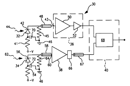
As illustrated in FIG. 2, the present invention provides a high speed
differential optoelectronic receiver 30 that achieves higher data rate
performance
s than the conventional balanced detector optoelectronic receiver of the prior
art and
which is capable of using resistively terminated photodiodes, thus allowing
for
impedance matching to transmission lines.
The receiver 30 includes a pair of photodetectors 32 and 34, amplifiers 36
and 38 and an output circuit 40. The photodetector 32 has its anode connected
to through a bias resistor 41 to a negative DC voltage (-V). A high frequency
bypass
capacitor 70 also connects this anode to ground 46 to provide a path for the
high
speed currents induced in the photodiode 32 by the high speed optical signal
44.
The bias resistor 41 prevents these currents from trying to drive the negative
DC
voltage (-V). Ordinarily current is not drawn so the potential on the
photodetector
~s 32 is the same -V as is applied to the resistor. Its cathode 42 is
connected to an
input terminal 43 of the amplifier 36. By reverse biasing the photodetector 32
its
internal depletion region is increased which in turn increases the distance
between
its contacts thus decreasing its associated capacitance. The photodetector 32
serves to convert an incident amplitude modulated optical signal 44 into an
zo electrical drive current for subsequent amplification by the amplifier 36.
The
amount of current created is dependent upon the amount of incident light in
the
optical signal 44. An impedance matching resistor 45 is connected across
photodetector 32 between the cathode 42 and ground 46 that develops an
-6-
CA 02289400 1999-11-12
_,V Docket No. 11-0974
electrical drive voltage from the electrical drive current generated by the
photodetector 32. A transmission line 48, preferably a RF transmission line or
a
coaxial cable, is connected between the resistor 45 and the input terminal 43.
The
amplifier 36 comprises two amplifiers 50 and 52 connected in cascade. The
s amplifiers 50 and 52 each serve to amplify and invert the electrical drive
voltage
applied to the input terminal 43. The effect of the two cascaded amplifiers is
that no
inversion results.
Similarly, the photodetector 34 has its anode connected through a bias
resistor 54 to the negative DC voltage -V and also to a high frequency bypass
io capacitor 72, and its cathode 56 connected through a transmission line 58
to an
input terminal 60 of the amplifier 38. This reverse bias arrangement reduces
the
capacitance associated with the photodetector 34. The photodetector 34 must be
connected with the same polarity as that of photodetector 32 and converts an
incident amplitude modulated optical signal 62 into an electrical drive
current with a
Is magnitude corresponding to the amount of light in the optical signal 62.
This
electrical drive current develops an electrical drive voltage across an
impedance
matching resistor 64 connected across the photodetector 34 between the cathode
56 and ground 46. This electrical drive voltage is applied to the amplifier 38
through the transmission line 58. The transmission lines 48 and 58
advantageously
2o allow the photodetectors 32 and 34 to be remote or separated from the
amplifiers
36 and 38, respectively, without compromising high speed performance. The
transmission lines 48 and 58 may be conventional coaxial cables or impedance
matched microstrip or stripline transmission lines. The amplifier 38 is of the
high
_7_
CA 02289400 1999-11-12
. _. J~ Docket No. I I-0974
gain type and serves to invert and amplify the electrical drive voltage
applied to its
input 60. The amplification it provides is equal to or slightly greater than
that
provided by the cascaded amplifiers 50 and 52. Preferably, the output of the
amplifier 38 is connected through an attenuator 66 and a delay line 67 to the
output
s circuit 40. If the amplification provided by the amplifiers 50 and 52 is
greater than
that provided by amplifier 38 then the attenuator 66 would be included in the
circuit
after the amplifier 52. The attenuator 66 enables the magnitude of the
amplified
signal to be adjusted so that the magnitude of the amplified signals in the
two paths
are equal. The delay line is preferably a coaxial cable and serves to adjust
the
to phase of the amplified signal and is of a length sufficient to cause delay
so that the
two amplified signals are in phase. Hence the amplified signal at the output
of the
single stage amplifier 38 is adjusted to be in phase with and of the same
magnitude
as that from the cascaded double stage amplifier 36. The output circuit 40
comprises a resistive power combiner 68 having its input terminals connected
to the
Is outputs of the amplifier 36 and the coaxial cable 67 and provides a single
ended
load.
In the preferred embodiment, the photodetectors 34 and 36 are resistively
terminated photodiodes that include 50 ohm termination resistors 45 and 64,
respectively, and are commercially available from Lasertron, Inc. as model
QDMH
20 1-055. Such photodiodes have an internal capacitance of about 0.4
picofarads. By
having each photodetector drive its own electronic amplifier it is possible to
use
commercial packaged photodiodes that are resistively terminated. This
arrangement also allows the photodiodes to be individually biased to unique
_8_
CA 02289400 1999-11-12
.W Docket No. 1 I-0974
voltages enabling their frequency response to be individually tailored for a
particular
application. If the photodiodes are not resistively terminated the photodiode
current
is applied directly to drive the respective amplifiers and the application of
transmission lines will not be possible. The transmission lines 48 and 58 are
s coaxial cables having a 50 ohm characteristic impedance. The amplifiers 36
and
38 are conventional RF amplifiers. One must have inverting gain relative to
the
others. The double stage (non-inverting) amplifier 36 is manufactured by SHF
Design of Berlin, Germany and designated as Model 90. The single stage
amplifier
38 is manufactured by Anritsu Company of Japan and designated as Model
~o A3HB3102. The resistive power combiner 68 is manufactured by Wienschel and
designated as Part 1580. It provides an input impedance back toward the
amplifiers 36 and 38 of 50 ohms and an output impedance at the output of
circuit
40 of 50 ohms.
In operation the incident amplitude modulated optical signals 44 and 62 must
Is be complementary. Complementary means that any increase in light in one
photodetector is accompanied by a decrease of light in the other
photodetector.
Since the light is complementary, the photo current created by the
photodetector 32
drives its amplifier 36 solely since there is no common electrical connection
to the
photodetector 32. Similarly, the photo current created by the photodetector 34
2o drives amplifier 38 solely. By orienting both photodetectors with the same
polarity
on the input of the amplifiers, an enhanced performance electronic amplifier
can be
used since it only has to sink the photo currents flowing in one direction
from the
photodetectors. Moreover, the capacitance appearing at the input of each of
the
-9-
CA 02289400 1999-11-12
.V Docket No. 1 I-0974
amplifiers is only that associated with its corresponding photodetector. This
is only
one-half the capacitance appearing at the input of the amplifier of the prior
art
commercial optoelectronic receiver. The enhanced electronic amplifier
performance and reduced capacitance enables this inventive differential
s optoelectronic receiver to achieve higher data rate performance.
When the incident amplitude modulated optical signal 44 is applied to the
photodiode 32 it creates an electrical current having a magnitude proportional
to the
intensity of the light in the first signal 44. The electrical current is
converted to a
voltage by the resistor 45, which voltage is applied to the input 43 of
amplifier 36.
to Similarly, when a complementary incident amplitude modulated optical signal
62 is
applied to the photodiode 34 it creates a current having a magnitude
proportional to
the intensity of the light in the second complementary signal 62. The current
is
converted to a voltage by the resistor 64 which is applied to the input 60 of
amplifier
38. Similarly, the currents applied to the electronic amplifier 36 and 38 are
both in a
Is sinking manner or direction. The amplifiers 36 and 38 amplify the signals
at their
inputs with amplifier 38 also providing an inversion and by means of the
attenuator
66 and delay line 67 which attenuates the amplitude and delays the phase
respectively the output signal from the amplifier 38 creates signals to the
output
circuit 40 that have equal amplitude and are in phase. A single ended signal
is
2o provided at the output of the impedance matched output circuit.
As will be recognized the receiver is a linear system. This produces a
differential output signal that is proportional to the difference between the
two
signals applied to the input terminals of the amplifiers 36 and 38. This
difference is
- ~o-
CA 02289400 1999-11-12
.<W Docket No. 11-0974
in the algebraic sense such that for equal amplitudes the magnitude is twice
that of
one of the signals. Also the photodetectors could have a positive supply
voltage
applied to their cathodes with both anodes providing the input to the
amplifiers.
This receiver provides noise rejection capability because the incident optical
s signals must be complementary. If the incident optical signals are both
present or
both absent then there would not be an output.
Referring now to FIG. 3 and to FIG. 4, an alternative embodiment of the
present invention is shown. FIG. 4 illustrates the schematic diagram of an
integrated circuit embodiment of the high speed differential optoelectronics
~o receiver, generally designated by the numeral 80. The difference between
this high
speed differential optoelectronic receiver 80 and the optoelectronic receiver
shown
in FIG. 2 is that it includes a differential amplifier 82 having inputs 84 and
86 and
outputs 88 and 90. FIGs. 3 and 4 contain many of the same elements as were
shown and described in FIG. 2 and like numerals have been provided for those
i s elements.
Briefly, the two current signals applied to the inputs 84 and 86 are treated
as
a differential electronic input. As will be described subsequently, the
differential
amplifier 82 is also referred to as a differential transimpedance amplifier
and utilizes
two internal identical amplifiers for each input to give two complementary
outputs
20 (see the mirror circuits in the upper and lower portions of FIG. 4). This
is in contrast
to the embodiment presented in FIG. 2 where amplifier 38 provided an inverted
output relative to amplifier 36. The two internal identical amplifiers are
operated
differentially by connecting a common potential, known as a common mode
CA 02289400 1999-11-12
,W Docket No. I 1-0974
voltage, between the amplifiers. The signals appearing on the outputs 88 and
90
are complementary and proportional to the difference between the electrical
signals
appearing on the inputs 84 and 86, respectively. As in the previous
embodiment,
the incident optical signals 44 and 62 are complementary and amplitude
modulated
s and may be either of an analog or a digital type.
The optoelectronic receiver 80 includes photodetectors 32 and 34,
termination resistors 45 and 64 and the differential amplifier that comprises
two sets
of four stages, namely common base input stages 92, emitter follower stages
94,
differential gain stages 96 and common base output stages 98. The amplifier 82
to comprises the integrated circuit, which is formed of a semiconductor
material. The
amplifier is a heterojunction bipolar transistor (HBT) dual input
transimpedance
amplifier CHAMP) and has been fabricated from indium phosphide and gallium
arsenide. Similar amplifiers also could be fabricated from silicon, silicon
germanium
or any other semiconductor process. The photodetectors 32 and 34 and
Is termination resistors 45 and 64 are purchased commercially and are not part
of the
integrated circuit. Blocking capacitors 100 and 102 prevent current developed
on
the emitters of transistors Q1 and Q2 in the input stage 92 from flowing into
the
termination resistors 45 and 64, respectively, to ground. The blocking
capacitors
100 and 102 have a capacitance sufficient to prevent such current flow over
the
2o entire frequency range of operation and are preferably 3 microfarads. The
high
frequency bypass capacitors 70 and 72 enable both anodes of the photodetectors
32 and 34 to be reversed biased with the -V DC potential while providing a
path for
- 12-
CA 02289400 1999-11-12
-.W Docket No. 11-0974
any AC signals to ground. Generally this bypass capacitor is part of the
commercial
photodetector-termination resistance package.
In the amplifier 82 the common base input stage 92 uses common base
transistors Q1 and Q2 to create low input impedance that is matched to the
input
s impedance provided by the termination resistors 45 and 64, which is
important
because the photodiode capacitance affects the amplifier bandwidth as
previously
described. Transimpedance resistors R1 and R2 at the collector outputs of Q1
and
Q2 convert the photodiode currents generated by the photodetectors 32 and 34
to
voltages without increasing the RC time constant of the circuit. The high
to impedance outputs of Q1 and Q2 are buffered by the Darlington-configured
emitter
follower stage 94 having transistors Q3 and Q4 with a loss of about 1 dB. The
emitter follower outputs are loaded with resistors R3 and R4 to AC virtual
ground
nodes 104 and 105 and provides impedances that are matched to that of the
differential gain stages 96. This helps to stabilize the emitter follower
stage 94 and
is reduce frequency domain peaking.
The differential gain stages 96 includes transistors Q5 and Q6 to generate a
differential output signal proportional to the difference between the two
input
currents at inputs 84 and 86. This also provides an additional 5 dB of gain.
Resistors R5 and R6 provide emitter degeneration that increases the linearity
and
2o bandwidth of the stages at the cost of lower gain. The differential stages
output
current is buffered by the common base output stages 98 that comprise
transistors
Q7 and Q8. This increases amplifier bandwidth by reducing the Miller
capacitance
associated with the transistors. The outputs 88 and 90 are fully back
terminated
-13-
CA 02289400 1999-11-12
..<W Docket No. 11-0974
with 50 ohm resistors 106 and 108 to improve output return loss and provides a
differential output signal that is proportional to the two signals applied to
the input
terminals 84 and 86.
The emitter follower and differential gain stages 94 and 96 are biased with
s simple current mirror current source circuits 120, 122, 124 and 126. The
current
sources are programmable and controlled to have a magnitude determined by the
reference voltages REF 10, REF 11, REF 20 and REF 21, respectively. The
current setting resistors (not shown) for these current sources are connected
to
separate pads for maximum flexibility in circuit evaluation.
to As shown in FIG. 3, coaxial cables 48 and 58 could be inserted to separate
the amplifier from the photodetectors. Also, it should be noted that
individual
photodetector die without resistive termination can be mounted directly on the
surface of, or fabricated as part of the integrated circuit amplifier 82
without the use
of transmission lines, coaxial cables or the like.
is Obviously, many modifications and variations of the present invention are
possible in light of the above teachings. Thus, it is to be understood that,
within the
scope of the appended claims, the invention may be practiced otherwise than as
specifically described above.
- 14-