Note: Descriptions are shown in the official language in which they were submitted.
CA 02289501 2003-05-15
GYRATOR WITH LOOP AMPLIFIERS CONNECTED TO INDUCTIVE ELEMENTS
TECHNICAL FIELD
The present invention relates to a gyrator forming a resonant
circuit.
BACKGROUND ART
In modern communications systems, low phase noise oscillators are
required as an integral part of the process of transporting data. While
10 ever increasing data rates are employed, it becomes more and more
difficult to meet the requirements for low phase noise. In many
applications, the requirement for low phase noise has been met by means
of oscillators with fixed frequencies or narrow band tuning range which
utilizes some form of a resonant tank circuit of high quality factor (Q).
15 The tank circuit limits the noise bandwidth of the oscillator circuit. In
applications where a wider tuning range is needed, it is possible to use a
multiple of such oscillators with overlapping tuning ranges. Such
arrangements, however, are cumbersome and an alternative class of broad
tuning range low noise integrated oscillator is desirable.
20 United States Patent 5,371,475 granted to A.K.D. Brown on
December 6, 1994 describes the principles of operation of a class of low
noise oscillators, which are known as gyrators. The principles of a
conventional gyrator is fully described in the patent. United States Patent
5,483,195 granted to A.K.D. Brown on January 9, 1996 describes means of
25 obtaining a broad tuning range for a gyrator oscillator which is
independent of process and temperature variations. The prior gyrator
needs improvement on achievement of broad tuning range concurrently
with low phase noise, for some applications. A paper by A.K.D. Brown
entitled "An integrated low power microwave VCO with sub-picosecond
30 phase fitter", IEEE 96CH35966, IEEE BCTM 10.3, pp. 165-168 describes
phase noise analysis of gyrators.
SUMMARY OF THE INVENTION
It is an object of the present invention to provide a gyrator with an
35 improved phase noise performance.
According to one aspect of the present invention, there is provided
a gyrator forming a resonant circuit comprising: a loop having ports 1 and
CA 02289501 1999-11-10
WO 99/53614 PCT/CA99/00255
2
2, each port having two terminals, the loop comprising loop-connected
first and second amplifiers, the gain of the loop being mare than unity;
capacitive means for coupling the terminals of the respective ports,
thereby causing effective nodal capacitance in each port and effective
nodal inductance in the other port, the capacitance and inductance
determining the resonant frequency of the gyrator; and inductive means
for coupling the terminals of the respective ports, thereby the effective
nodal capacitance in the respective port being varied.
For example, the capacitive means is capacitance elements. Each of
them is connected between the terminals of each port, or between the
terminal of one port and the respective terminal of the other port. The
inductive means is inductance elements. Each of them is connected to the
respective terminal of the port. The effective nodal capacitance is reduced
by the inductance elements. The gyrator oscillatory frequency exceeds the
maximum oscillation frequency possible in a gyrator without inductance
elements.
The inductive elements act to discriminate against injected power
supply noise, resulting in improved oscillator phase noise. The do voltage
drop of the inductor is less than that of the original resistive load,
resulting in larger linear oscillations and reduction in the oscillator phase
noise.
According to another aspect of the present invention, there is
provided a gyrator forming a resonant circuit comprising: a loop having
ports 1 and 2, each port having two terminals, the loop comprising loop-
connected first and second amplifiers, the gain of the loop being more
than unity; capacitive means for coupling the terminals of the respective
ports, thereby causing effective nodal capacitance in each port and
effective nodal inductance in the other port, the capacitance and
inductance determining the resonant frequency of the gyrator; and
inductive means for coupling the terminals of the respective ports, thereby
the effective nodal capacitance in the respective port being varied. The
first and second amplifiers of the loop comprises first and second
differential amplifiers, respectively, each differential amplifier having
inverting and non-inverting inputs and outputs. The loop comprises
amplifier coupling means for coupling the inverting and non-inverting
outputs of the first differential amplifier to the non-inverting and
inverting inputs of the second differential amplifier, respectively, and for
SUBSTTTUTE SHEET (RULE 26)
CA 02289501 1999-11-10
WO 99153614 PCT/CA99100255
3
coupling the inverting and non-inverting outputs of the second
differential amplifier to the inverting and non-inverting inputs of the first
differential amplifier, respectively, the gain of the loop comprising the
first
and second differential amplifiers being greater than unity. Each of the
first and second differential amplifiers has a generally 90 degree phase
shift between its input and output at the resonant frequency.
For example, each of the first and second differential amplifiers
comprises a variable transconductance amplifier. The variable
transconductance amplifier comprises tuning means for tuning with a
differential voltage. The variable transconductance amplifier further
comprises automatic gain control means which is electrically separated
from the tuning means. The tuning control means is functionally
dependent upon the automatic gain control means. The automatic gain
control means comprises a fast acting control loop to ensure oscillation
stability under rapid tuning variations.
The gyrator further comprises a fast control loop and a slower
control loop for precision vernier adjustment of an output signal level. An
output oscillation frequency of the gyrator responds to the variation of the
transconductance of the transconductance amplifiers.
BRIEF DESCRIPTION OF THE DRAWINGS
Embodiments of the present invention will now be described by
way of example with reference to the accompanying drawings in which:
Figure 1 illustrates a prior art gyrator;
Figure 2 illustrates a model of a prior art gyrator;
Figure 3 illustrates a model of another prior art gyrator;
Figure 4 illustrates a model of an embodiment of a gyrator
according to the present invention;
Figure 5 illustrates a model of another embodiment of a gyrator
according to the present invention;
Figure 6 is a graph of angular frequency - gyrator nodal impedance;
Figure 7 illustrates a model of another embodiment of a gyrator
according to the present invention;
Figure 8 illustrates a model of another embodiment of a gyrator
according to the present invention;
Figure 9 is a schematic diagram of an embodiment of a gyrator
according to the present invention;
SUBSTITUTE SHEET (RULE 2G)
CA 02289501 2003-05-15
4
Figure 10 is a block diagram of a variable linear transconductance
amplifier used in the gyrator shown in Figure 9;
Figure 11 is a schematic diagram of a tuning circuit used in the
transconductance amplifier shown in Figure 10;
5 Figure 12 is a schematic diagram of a variable gain linear
transconductance amplifier used in the transconductance amplifier shown
in Figure 10;
Figure 13 is a schematic diagram of an automatic gain control
circuit used in the transconductance amplifier shown in Figure 9;
10 Figure 14 is a schematic diagram of another embodiment of a
gyrator according to the present invention;
Figure 15 is a schematic diagram of a gyrator according to another
embodiment of the present invention;
Figure 16 is a schematic diagram of a transconductance amplifier
15 used in the gyrator shown in Figure 15;
Figure 17 is a schematic diagram of a peak detector used in the
transconductance amplifier shown in Figure 16; and
Figure 18 is a schematic diagram of an output buffer and bias
circuit used in the transconductance amplifier shown in Figure 16.
BEST MODE FOR CARRYING OUT THE INVENTION
I. Prior Art
I-1. Gyrator
Figure 1 shows a prior art gyrator including two amplifiers A1 and
A2, the gains of which are usually the same. The inverting and non-
inverting outputs ON and OP of the amplifier A1 are connected to the
inverting and non-inverting inputs IN and IP of the amplifier A2,
respectively. The inverting and non-inverting outputs ON and OP of the
amplifier A2 are connected to the non-inverting and inverting inputs IP
30 and IN of the amplifier Al, respectively. The amplifiers A1 and A2 are
coupled to form a loop, the total gain of which is greater than unity. The
outputs of the amplifiers A1 and A2 are ports 1 and 2 of the gyrator,
respectively. An example of a gyrator is described in United States Patent
Serial Number 5,483,195.
I-2. Gyrator Model
CA 02289501 2003-10-21
Figure 2 shows a model of a prior art gyrator having shunt nodal
capacitors. The gyrator has two ports - Port 1 and Port 2. Each port has
two terminals and a shunt nodal capacitor C is connected between the two
terminals which are connected to a terminal of supply voltage Vcc via load
5 resistors R. Figure 3 shows another prior art gyrator having Miller
feedback nodal capacitors C, instead of shunt nodal capacitors. The
principles of operation of these gyrators have been fully described in
United States Patent No. 5,371,475. Two semi-orthogonal conditions exist
for the gyrator of Figure 1 which are required for unity loop gain at which
the gyrator will oscillate. Two possible topologies exist for the basic
gyrator circuit as shown in Figures 2 and 3, for which identical unity gain
conditions exist as:
cep = g / (C + GD) (1)
D = G / (cope C) (2)
Here, coo is a resonant angular frequency, g is a gyrator amplifier
transconductance, G is a load loss admittance, D is an amplifier built in
delay.
These gyrators are unique in the sense that they emulate a high Q
parallel LRC resonant tank circuit with measured Q factors of 250, without
employing a physical inductor. The inductor of the resonant circuit is
obtained by transforming the capacitive reactance on one of the gyrator
25 nodes so that it appears as an inductor in parallel with the capacitive
reactance on the other node. While this feature is highly desirable in
supplying a highly selective resonant circuit which suppresses the circuit
noise, it is less effective in its ability to suppress unwanted noise from
external sources. In this respect, the circuit is twice as sensitive to the
30 effects of externally induced noise as compared to a conventional
resonator with passive inductor. This is important because such high
frequency noise can modulate the oscillator frequency and alias down into
the frequency band of interest.
It will be apparent that the gyrator circuit would be improved if the
35 capacitors could be replaced by inductors: thus one could notionally
transform the inductive reactance at one node into a capacitive reactance
at the other node and so form a resonant circuit. A mathematical
CA 02289501 1999-11-10
WO 99/53614 PCT/CA99/00255
6
treatment of this procedure, however, results in the requirement that the
value of the inductors required for oscillation are finite and negative.
Thus, this is not a practical solution.
With reference to Figure 2, the capacitive admittance at either node
(nodal admittance Y) is described as:
Y=G+jwC (3)
The net loss admittance is capacitive. This is a necessary condition
for the gyrator to oscillate, as the analysis for a purely inductive circuit
shows.
II. First Embodiment Gxrator
II-1. Gyrator Model
Figure 4 shows a model of an embodiment gyrator with shunt
nodal capacitors and load inductors. In Figure 4, the gyrator has two
ports - Port 1 and Port 2, each port having two terminals. Each port is
provided with a shunt nodal capacitor C between its terminals which are
connected to a terminal of supply voltage Vcc via load inductors L. Figure
5 shows a model of another embodiment gyrator having Miller feedback
capacitors and load inductors. Figure 6 illustrates a nodal impedance Zn
as function of angular frequency w. The capacitive admittance at either
port (nodal admittance Y) is described as:
Y=G+jwC+1 /jwL (4)
Y=G+j(wC-1 / wL) (5)
Note the admittance on the imaginary axis can be either capacitive
or inductive depending upon the relative magnitude of the capacitance C
and inductance L, and, most importantly; the magnitude of the angular
frequency w. At the natural resonant frequency wp of the parallel C and L,
their loss admittances are equal, so that the net loss admittance is G
(resistive) and the circuit will not oscillate. At frequencies above the
frequency wp, the capacitive term dominates and the net admittance is
capacitive. At this point it is essential to note that the presence of the
inductance effectively reduces the capacitive admittance. Therefore,
SUBSTTTIJTE SHEET (RULE 26)
CA 02289501 1999-11-10
WO 99153614 PCTlCA99100255
7
introduced is equivalent capacitance C' which determines new oscillating
frequency wow of the gyrator according to Equation 1 and Equation 2 such
that:
C' = C - (1 / w2L) (6)
From Equation 6, it is possible to reduce the effective nodal
capacitance Yn by partially cancelling it with the inductor, giving rise to
the following desirable attributes:
(1) The oscillatory frequency of the gyrator can be raised higher
than that attainable for the conventional gyrator of Figures 2 and 3 by
introducing a parallel inductor to partially cancel the nodal capacitance as
in Figure 4.
(2) Alternatively a larger nodal capacitance can be employed at
the same oscillator frequency by introducing a parallel inductor to
partially cancel the nodal capacitance.
The ability to raise the oscillator frequency is very useful when the
desired frequency is otherwise unattainable in a conventional gyrator due
to parasitic capacitances.
The ability to increase the nodal capacitance is desirable when the
gyrator nodal capacitance largely consists of non-linear parasitic
capacitance which lowers the Q factor of the gyrator. By introducing a
shunt linear capacitor and a shunt inductor, the net capacitance is more
linear since the parasitics are largely swamped, while the same resonant
frequency is attained.
In addition, the shunt load resistor used in the conventional gyrator
appears in parallel with the added inductor and an equivalent Q factor can
be calculated for the inductor resistor combination. Conveniently, the
shunt resistor inductor combination can be replaced by a series
combination of the inductor and a resistor having the same combined Q
factor. The value of the series resistor is calculated to achieve the same Q
factor as for the shunt inductor resistor combination. In practice,
integrated inductors can be designed having the required Q factor without
the requirement for an additional series resistor.
Figure 6 shows the nodal impedance as a function of angular
frequency, where cep is the resonant angular frequency and wosc is the
SUBSTrTUTE SHEET (RULE 26)
CA 02289501 1999-11-10
WO 99153614 PCTICA99I00255
8
oscillating angular frequency. The oscillating angular frequency wow is
shifted from the resonant angular frequency wo by C'.
Figure 7 shows a model of an embodiment gyrator wherein nodal
shunt capacitances are combination of parasitic capacitances C and
additional capacitances Cad. The gyrator improves its linearity. Figure 8
shows a model of an embodiment gyrator wherein nodal shunt
capacitances are combination of capacitances C and additional
capacitances Cad. The gyrator increases its oscillation frequency and
improves its linearity.
Three examples will be given below for the comparison purpose.
Example 1:
Prior Art Gyrator of Figure 2
Resonant Frequency =1 GHz
Nodal Capacitance C =1 pF
Shunt Load Resistance = 350 S'Z
Embodiment G~,~rator of Fire 4
Oscillation Frequency = 2 GHz
Inductance L = 8.7 nH
(Inductor's Q factor = 3.3)
Note that the parallel resonance frequency of the 1 pF capacitor and
8.4 nH inductor is 1.73 GHz and the equivalent capacitive reactance of the
parallel combination at the 2 GHz oscillation frequency is 0.25 pF. In this
example, the oscillating angular frequency wow is shifted from the
resonant angular frequency wo to a higher frequency (see Figure 6).
Example 2:
Prior Art G~,rator
Resonant Frequency =1 GHz
Nodal Capacitance C =1 pF
(consisting of non-linear circuit parasitics)
Shunt Load Resistance = 350 S2
SUBSTITUTE SHEET (RULE 2~
CA 02289501 1999-11-10
WO 99153614 PCTICA99100Z55
9
Embodiment Gxrator (see Figure ~
Oscillation Frequency =1 GHz
Inductance L =12.7 nH
(Inductor's Q factor = 4.38)
Additional Shunt Capacitance Cad = 2 pF
Note that the self resonant frequency of the parallel inductor
capacitor combination is 0.816 GHz. The equivalent nodal capacitance is
still 1 pF. In this example, the oscillating angular frequency w~ is
substantially the same as the resonant angular frequency wo.
Example 3:
Prior Art Gyrator
Resonant Frequency =1 GHz
Nodal Capacitance C =1 pF
Shunt Load Resistance = 350 SZ
Embodiment (see Figure 8)
Oscillation Frequency = 2 GHz
Inductance L = 3.6 nH
(Inductoi s Q factor = 7.73)
Additional Shunt Capacitance Cad =1 pF
In this example, the gyrator oscillation frequency can be increased
to a 2 GHz oscillation frequency while at the same time doubling the nodal
capacitance linearity.
Thus, the ability to double the gyrator frequency while doubling
the nodal capacitance can be achieved by replacing the shunt nodal load
resistor with a shunt lossy inductor which at the same time achieves the
purpose of discriminating against injected power supply noise. The
filtering action of the inductor depends on the inductor capacitor
combination and is enhanced where the nodal capacitance is increased. In
the case of example 2, the attenuation of high frequency power supply
noise increases at 12 dB per octave above 1 GHz as compared to the
unmodified gyrator with 6 dB per octave. Thus, the improved gyrator has
SUBSTITITTE SHEET (RULE 26)
t
CA 02289501 1999-11-10
WO 99/53614 PCT/CA99I00255
43.6 dB attenuation of 10 GHz noise as compared to the unmodified
gyrator with 27.2 dB.
A further advantage of replacing the resistive loads with lossy
inductive loads is that the passive inductors can store energy, thus
5 permitting voltage excursions above the supply rail. Also, of great
advantage is the increased voltage swing possible with a given power
supply since the do voltage drop due to the 350 SZ load resistor is no
longer present.
10 II-2. Detailed Circuit of the First Embodiment Gyrator
Referring to Figure 9 which shows a gyrator according to an
embodiment of the present invention, the gyrator includes two variable
linear transconductance amplifiers (VLTAs) 2111 and 2112 having the
same circuit configuration and an automatic gain control (AGC) circuit
213. Each of the VLTAs 2111 and 211 has inverting and non-inverting
inputs IN and IP and inverting and non-inverting outputs ON and OP.
Each VLTA provides differential output voltage between its non inverting
and inverting outputs OP and ON in response to differential input voltage
fed between its non-inverting and inverting inputs IP and IN. The outputs
OP and ON of the VLTA 2111 are connected to the inputs IN and Il' of the
VLTA 2112 via capacitors 2171 and 2172, respectively. The outputs OP and
ON of the VLTA 2112 are connected to the inputs IP and IN of the VLTA
2111 via capacitors 2191 and 2192, respectively. Each of the capacitors
2171, 2172, 2191 and 2192 has capacitance Cc. The inputs IP and IN of the
VLTA 2111 are connected to a bias terminal 221 to which bias voltage Vb1
is fed, via resistors 223P and 223N, respectively. The inputs IP and IN of
the VLTA 2111 are connected to the ground terminal via capacitors 225P
and 225N, respectively. The outputs OP and ON of the VLTA 2111 are
connected to a terminal 227 of supply voltage Vcc (e.g., +5 V), via
inductors 229P and 229N, respectively. The inputs IP and IN of the VLTA
2112 are connected to the bias terminal 221 via resistors 231P and 231N,
respectively. The outputs OP and ON of the VLTA 2111 are connected to
other inputs AP and AN of the VLTA2, respectively. The outputs OP and
ON of the VLTA 2112 are connected to other inputs AN and AP of the
VLTAl, respectively. The inputs IP and IN of the VLTA 2112 are
connected to the ground terminal via capacitors 233P and 233N,
respectively. Each of the capacitors 225N, 225P, 233N and 233P has
SUBSTITUTE SHEET (RULE 2~
CA 02289501 1999-11-10
WO 99153bI4 PCTICA99100255
11
capacitance Ca. The outputs OP and ON of the VLTA 2112 are connected
to the terminal 227 via inductors 235P and 235N, respectively. Peak
detection terminals Pl and P2 of the VLTAs 2111 and 2112 are connected
to the respective peak detection terminals P1 and P2 of the AGC circuit
213, the AGC terminal of which is connected to AGC terminals of VLTAs
2111 and 2112.
The outputs OP and ON of the VLTA 2111 are defined as "Port 1"
and the outputs OP and ON of the VLTA 2112 are defined as "Port 2". The
nodal capacitance of the each port is a series of the two capacitances Cc
and the two capacitances Ca. The VLTAs 2111 and 2112 are biased
through the resistors 223N, 223P and 231N, 231P by the bias voltage Vbl.
The VLTAs 2111 and 2112 develop large voltage swings in the inductors
229P, 229N, 235P and 235N. The gain of the VLTA 2111 is the same one as
that of the VLTA 2112. A total gain of a loop comprising the VLTAs 2111
and 2112 is greater than unity. Each of the VLTAs 2111 and 2112 has a 90
degree phase shift between its input and output at a resonant frequency.
Quadrature output voltage Voscl and Vosc2 are provided from Ports 1
and 2, respectively. The capacitors 225N, 225P, 233N and 233P of the
capacitance Cc attenuate the signals at the inputs of the VLTAs 2111 and
2112, so as to avoid overloading the VLTAs.
Figure 10 shows the VLTA which includes a tuner 311 and a
variable gain linear amplifier (VGLA) 321. The non-inverting and
inverting inputs IP and IN of the VLTA are connected to non-inverting
and inverting inputs IP and IN of the VGLA 321, respectively, the non-
inverting and inverting outputs OP and ON of which are connected to the
non-inverting and inverting outputs OP and ON of the VLTA. Tuning
terminals FP and FN of the VGLA 321 are connected to the tuning
terminals FP and FN of the tuner 311, the tuning inputs TP and TN are
connected to the tuning inputs of the VLTA. The inputs AP and AN of the
VLTA are connected to the outputs OP and ON of the tuner 11. The AGC
terminals of the tuner 311 and VGLA 321 are connected to the AGC
terminal of the VLTA to which AGC voltage Vagc is fed. The tuning
inputs TP and TN are provided with differential tuning adjustable voltage
Vad (the source of which is not shown). Differential tuning input voltage
Vti is fed from the forting terminals FP and FN of the VGLA 321 to the
tuning terminals FP and FN of the tuner 311.
SUBSTITUTE SHEET (RULE 26)
CA 02289501 1999-11-10
WO 99153614 PCT/CA99100255
12
The tuner 311 and the VGLA 321 are combined to create a linear
tuning arrangement. This technique is based on the vector summation of
the amplifier output current with a variable quadrature feedback signal,
so as to alter the transconductor amplifier delay and hence the gyrator
frequency.
Figure 11 shows the tuner 311 of Figure 10. The following
description assumes, for simplicity and purely by way of example, that the
FETs referred to are P-channel MOSFETs (metal oxide semiconductor field
effect transistors} and the transistors referred to are NPN-type bipolar
transistors. In Figure 11, the tuner 311 includes two differential amplifier
circuits of transistors 411, 413, 415 and a resistor 417 and transistors 421,
423, 425 and a resistor 427. The tuning terminals FP and FN are connected
to the bases of the transistors 411, 423 and the bases of the transistors 413,
421, respectively. The non-inverting and inverting outputs OP and ON of
the tuner 311 are connected to the collectors of the transistors 411, 421 and
the collectors of the transistors 413, 423, respectively. The base of the
transistor 415 is connected to the base of a transistor 431, the base and
collector of which are connected to series-connected FETs 433, 435 and 437.
The emitter of the transistor 431 is connected to the ground terminal via a
resistor 439. Similarly, the base of the transistor 425 is connected to the
base of a transistor 441, the base and collector of which are connected to
series-connected FETs 443, 445 and 447. The emitter of the transistor 441 is
connected to the ground terminal via a resistor 449. The tuning inputs TP
and TN are connected to the gates of the FETs 443 and 433, respectively.
A resistor 451 of resistance RT is connected between the sources of the
FETs 433 and 443. The AGC terminal is connected to the base of a
transistor 453, the collector of which is connected to series-connected FETs
455 and 457. The emitter of the transistor 453 is connected to the ground
terminal via a resistor 459. The sources of the FETs 437, 447 and 457 are
connected to a terminal of do supply voltage Vcc (e.g., +5 volts). The
differential tuning adjustable voltage Vad is fed to the gates of the FETs
443 and 433. The differential tuning input voltage Vti is fed to the bases of
the transistors 411 and 413 from the collectors of which the differential
tuning output current Ito is provided.
The tuner 311 is essentially a four quadrant mixer which multiplies
the differential tuning input voltage Vti with the differential tuning
adjustable voltage Vad, so as to produce the differential tuning output
SUBSTTrUTE SHEET (RULE 26)
CA 02289501 1999-11-10
WO 99/53614 PCT/CA99/00255
13
current Ito having a variable amplitude. The base of the transistor 453 is
provided with the AGC voltage Vagc which is also fed to the VGLA 321.
Figure 12 shows the VGLA 321 of Figure 10. In Figure 12, the non-
inverting and inverting inputs 1P and IN of the VGLA 321 are connected
to the bases of transistors 511 and 513, the collectors of which are
connected to the emitters of transistors 515 and 517, respectively. The
emitter of the transistor 511 is connected to the collector of a transistor
519
and the base of a transistor 521. The emitter of the transistor 513 is
connected to the collector of the transistor 521 and the base of the
transistor 519. The emitters of the transistors 519 and 521 are connected to
the collectors of transistors 523 and 525, respectively, the emitters of which
are connected to the ground terminal via resistors 527 and 529,
respectively. The bases of the transistors 523 and 525 are connected to a
bias terminal 531 to which bias voltage Vb2 is fed. A gain control resistor
533 of resistance RG is connected between the emitters of the transistors
519 and 521. The collectors of the transistors 515 and 517 are connected to
the inverting and non-inverting outputs ON and OP of the VGLA 321,
respectively, and to the collectors of transistors 535 and 537, respectively.
The bases of the transistors 515 and 517 are connected to a bias terminal
539 to which bias voltage Vb3 is fed. The emitters of the transistors 535
and 537 are connected to the collector of a transistor 541, the emitter of
which is connected to the ground terminal via a resistor 543. The base of
the transistor 541 is connected to the AGC terminal. Each of the voltages
Vb2 and Vb3 is fed by a constant voltage source (not shown).
The VGLA 321 is a differential amplifier. The transistors 523 and
525 with the emitter degeneration resistors 527 and 529 operate as current
sources. The transistors 515, 517, 535 and 537 operate on the translinear
principle. The impedance seen at the emitters of the transistors 515 and
517 is very low, typically a few ohms, since it is the reciprocal of the
transconductance of these transistors plus some parasitic resistance. The
transconductance of this complete amplifier can be controlled by varying
the current sourced into the AGC input.
The transistors 519 and 521 are added in order to make the input
amplifier linear. The non-linear characteristic of the positive feedback pair
519 and 521 is the exact opposite of the non-linear characteristic of
transistors 511 and 513, thus creating a highly linear amplifier out of
transistors 511, 513, 519 and 521. The combination of this linear input
SUBSTITUTE SHEET (RULE 2~
CA 02289501 1999-11-10
WO 99/53614 PCTICA99/00255
14
amplifier and the linear output amplifier results in that the circuit of
Figure 12 is a highly linear high speed variable gain transconductance
amplifier. Voltage across the resistor 533 is used by the AGC circuit for
peak detection. The voltage (i.e., the differential tuning input voltage Vti)
between the tuning terminals FP and FN is used for tuning control.
Figure 13 shows an AGC circuit 213 of Figure 9. In Figure 13, a
resistor 611, a diode-connected transistor 613 and a resistor 615 are
connected in series between a terminal of the supply voltage Vcc and the
ground terminal. The AGC terminal is connected to the collector of the
transistor 613 and via a resistor 617 to the collectors of transistors 619,
621,
623 and 625, the emitters of which are connected to the ground terminal.
Both the terminals of the resistor 617 are connected to the ground terminal
via capacitors 627 and 629.
The AGC circuit 213 includes an offset circuit 630 wherein a resistor
631 and two diode-connected transistors 633 and 635 are connected in
series between the Vcc terminal and the ground terminal. The collector of
the transistor 633 is connected to the base of a transistor 637, the emitter
of
which is connected to the ground terminal via series-connected resistors
639 and 641. The collector of the transistor 637 is connected to the Vcc
terminal. The junction of the resistors 639 and 641 is connected to an
output OFS of the offset circuit 630.
The output OFS is connected to the bases of the transistors 619, 621,
623 and 625 via resistors 643, 645, 647 and 649, respectively. Each of the
resistors 643, 645, 647 and 649 has resistance Rb. The bases of the
transistors 619 and 621 are connected to the peak detection terminals P1
and P2 of the VGLA 321 of the VLTA 2111 via capacitors 651 and 653,
respectively. Similarly, the bases of the transistors 623 and 625 are
connected to the peak detection terminals Pl and P2 of the VGLA 321 of
the other VLTA 2112 via capacitors 655 and 657, respectively.
The circuit 213 is a typical AGC arrangement to keep the VLTAs
2111 and 2112 operating in the linear region. Under start-up conditions,
the resistor 611 supplies current from the supply voltage Vcc to the
transistor 613. This establishes the bias AGC voltage Vagc which is fed to
the transistor 453 of the tuner 311 and the transistor 541 of the VGLA 321.
Once the oscillator signal reaches the required amplitude, the remaining
circuit of the AGC circuit 213 reduces the AGC bias voltage as described
below.
SUBSTTTIJTE SHEET (RULE 26)
CA 02289501 1999-11-10
WO 99!53614 PCT/CA99lOOZ55
The transistors 619, 621, 623 and 625 operate as peak detectors. The
resistors 643, 645, 647 and 649 permit a bias voltage to be presented to the
transistors 619, 621, 623 and 625, so as to bias these transistors off by a
predetermined offset voltage Vos derived from the offset circuit 630. If the
5 emitter current density in the transistors 633, 635 and 637 is the same,
then
the offset voltage Vos will be given by:
Vos = Vbe x Rdiv
10 Where Vbe is the base-emitter voltage of the transistors. Rdiv is a voltage
division ratio which is given by:
Rdiv = R6g1 / (R639 + 8641)
15 Where 8639 and R~1 are the resistances of the resistors 639 and 641,
respectively. The offset voltage Vos has a negative temperature coefficient
which is the same as that of a semiconductor diode: i.e., approximately -
0.002 x Rdiv v/C . In order to cancel the negative temperature coefficient,
and maintain a constant oscillator output voltage level, it is necessary to
increase the emitter current density of the transistor 637 relative to that of
the transistors 633 and 635. This will create an additional offset voltage at
the output OFS of the offset circuit 630 with a positive temperature
coefficient. This is an application of the band gap principle used in band
gap voltage generators. Finally one also has to take into account the ratio
of the peak emitter current density in the transistors 619, 621, 623 and 625
relative to the transistor 635, and typically this would be made unity to
avoid any additional temperature effects in the oscillator output level. It
has been assumed in this description that the temperature coefficient of
the resistance of the resistor 631 is zero. If this is not true, its effect
can be
cancelled by modifying the emitter current density ratio in the transistors
637 and 633 in conjunction with the ratio Rdiv.
In a typical arrangement, a 5.9 GHz oscillator with 5 Vp-p
differential quadrature outputs can be obtained with this oscillator. The
supply voltage must be at least 5 V relative to ground potential. Values of
the capacitors in Figure 9 are as follows:
Cc = 0.5 pF
Ca=l.5pF
SUBSTITUTE SHEET (RULE 267
CA 02289501 2003-05-15
16
The capacitor attenuator is thus 3:1 and a 2.5 volts single ended
swing at the output creates a 0.83 volt single ended swing at the input.
For the differential amplifier to operate in its linear range, the value
of the resistor RG multiplied by the current sunk in transistors 523, 525
must exceed 2 volts. This is controlled by the bias voltage Vb2. In this
design, RG is 1 kS2, and the current sink is 2 mA. The AGC limited the
output to 2.6 Vp-p, or 5.2 V differential peak-peak. The value of the
inductors is 2 nH with a Q factor of 6.4 at 5.9 GHz. The resistances of the
bias resistors 527, 529 and 543 are 10 kS2 and the bias voltage Vbl is 2.2 V.
The bias voltage Vb3 is 3 V.
Particular advantages of this embodiment are:
use of a capacitor divider circuit avoids delay in the coupled signal
so as to obtain maximum oscillator frequency and the capacitors perform a
dual function as the gyrator capacitors. In addition the capacitors increase
the efficiency of the VCO over that using a resistor attenuator;
the large signal swing output increases the carrier to noise ratio and
so reduces the phase noise;
the inductors inductance and quality factor are chosen for ease of
practical implementation at the oscillator frequency. Also since the
20 function of the inductor is to partially cancel the gyrator capacitance,
relatively large capacitors are used which swamp the non-linearities due
to the transistor parasitic capacitance.
Due to the low impedance presented by the shunt capacitors Ca at
the input of the amplifiers, and the relatively large input signal, the noise
performance of the amplifiers is good.
II-3. Second Embodiment
Figure 14 shows another embodiment including Miller feedback
capacitors 8111, 8112, 8113 and 8114 which are connected between the
30 respective non-inverting or inverting output and the inverting or non-
inverting input of the VLTAs. The capacitors 8111, 8112, 8113 and 8114 are
employed to further linearize the gyrator.
II-4. Limitations of the First and Second Embodiment Gyrators
35 The first and second embodiment gyrators are disclosed in
United States Patent Serial Number 6,025,765 filed by the same inventor
on April 8, 1998. In the gyrator, the advantages of inductive
CA 02289501 1999-11-10
WO 99/53614 PCTICA99I00255
17
loads for such gyrators are exploited. Specific improvements using
inductive loads include, larger amplitude signals, extended high
frequency performance, lower harmonic distortion with consequential
improved phase noise and discrimination against power supply noise: It
has been found however, that the improved gyrator has a practical
limitation imposed by the response time of the automatic output level
control. In the gyrator, the use of inductive loads required that the
inductance should be large enough that the inductive admittance is less
than the capacitive admittance of the gyrator nodal capacitors. If this
condition is met, the inductive admittance will partially cancel the
capacitive admittance. The overall nodal impedance is a reduced
capacitive reactance and this reduced capacitive reactance permits the
oscillator, for example, to oscillate at higher frequencies. The resultant
oscillator frequency is higher than the resonant frequency of the parallel
combination of the inductive load and the nodal capacitance. Such a
gyrator, with inductive loads has the capability of oscillating at the gyrator
resonant frequency, or alternatively, at the resonant frequency of the
parallel combination of the inductive load and nodal capacitance. To be
more precise, at the gyrator resonant frequency, the reduced nodal
capacitance of one node appears as a parallel inductance to the reduced
nodal capacitance of the other node and the quality factor of this resonant
combination can be at least as high as 250. On the other hand, the quality
factor of integrated inductors can be typically 3. Thus the quality factor of
the gyrator resonant circuit is about two orders of magnitude greater than
the quality factor of the resonant combination of inductive load and nodal
capacitance. Under normal operation, the gyrator chooses to oscillate at
the resonant frequency with the higher quality factor. However, under
some circumstances, where the oscillation is allowed to increase beyond
the normal linear range of the gyrator, increased harmonic distortion
lowers the gyrator quality factor and spurious oscillations at the frequency
of the resonant combination of inductive load and nodal capacitance can
result. An example of such a possibility occurs when the gyrator is
rapidly tuned from one frequency to another. Under these circumstances,
large changes in the loop gain of the gyrator can occur, causing the
amplitude to overshoot the linear region and allowing spurious
oscillations to build up. To' prevent this spurious operation in the first and
second embodiment gyrators, it is necessary to limit the rapidity with
SUBSTITUTE SHEET (RULE Z~
CA 02289501 1999-11-10
WO 99153614 PCT/CA99/001,55
18
which the gyrator is tuned. In practice, this imposes a limit on the
bandwidth of the filter of a phase locked loop, or similar application of the
gyrator.
III. Third Embodiment G,~rator
A third embodiment gyrator with inductive loads removes the
limitations of the first and second embodiment gyrators.
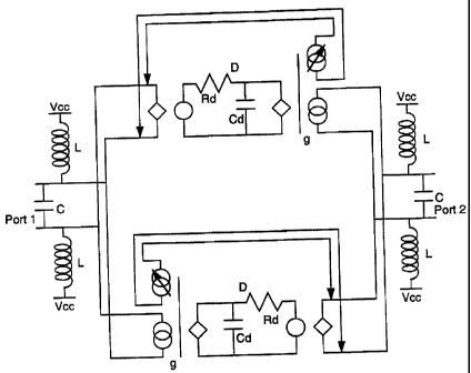
Referring to Figure 15 which shows a gyrator according to another
embodiment of the present invention, the gyrator includes two
transconductance amplifiers 901, 902, each having non-inverting and
inverting inputs and outputs. The non-inverting and inverting output
terminals OP and ON of the transconductance amplifier 901 are connected
to the non-inverting and inverting input terminals IP and IN of the
transconductance amplifier 902, respectively. The non-inverting and
inverting output terminals OP and ON of the transconductance amplifier
902 are connected to the inverting and non-inverting input terminals IN
and IP of the transconductance amplifier 901, respectively.
The possibility of separating the AGC circuit from the tuning
control arises out of the properties of a translinear amplifier. The output
stage of the gyrator variable linear transconductance amplifiers is a
translinear amplifier. In the above mentioned gyrator, the
transconductance is varied by variation of the tail current of the output
differential pair. However, the tuning arrangement also employed two
additional differential pairs whose inputs are connected in parallel with
the output differential pair, and whose outputs are arranged as
quadrature feedback signals to the alternate gyrator output. For tuning
purposes the tail currents of the quadrature differential pairs is varied.
Control of the transconductance also required that the tail currents of the
quadrature differential pairs should be varied. The resultant tuning
circuit of Figure 11 requires both tuning control signals as well as AGC
control.
Referring to Figure 16 which shows the transconductance amplifier
used in the gyrator, AGC control of the tail currents of the output
differential pair and the tuning quadrature differential pairs is eliminated,
so that the bias current of the output differential pair is fixed and the
tuning control is much simpler.
SUBSTITUTE SHEET (RULE 26)
CA 02289501 1999-11-10
WO 99/53614 PCTlCA99100255
19
Each of the transconductance amplifiers 901, 902 includes a tuning
amplifier 911, a transadmittance amplifier 912 and a translinear amplifier
913 which are cascaded between a terminal 227 of supply voltage Vcc (e.g.,
+5 V) and the ground terminal via transistors 915, 916. The tuning
amplifier 911 has non-inverting and inverting input terminals 917 and 918
which are connected~to the collectors of transistors 919, 920 and 921, 922,
respectively. The emitters of the transistors 919, 921 are connected to the
collector of a transistor 923, the emitter of which is connected to the
ground terminal via a resistor 924. The emitters of the transistors 920, 922
are connected to the emitter of a transistor 925, the emitter of which is
connected to the ground terminal via a resistor 926. The bases of the
transistors 919, 922 and 921, 920 are connected to the emitter of transistors
927 and 928, respectively, of the translinear amplifier 913. The emitters of
the transistors 927; 928 are connected to the bases of transistors 929, 930,
the emitters of which are connected to the ground terminal via a resistor
931. The bases of the transistors 927, 928 are connected to a bias input
terminal 932 of bias voltage Vb3. The collectors of the transistors 927, 928
are connected to the Vcc voltage terminal. The collectors of the transistors
929, 930 are connected to the voltage terminal via inductors 933, 934,
respectively. The collectors of the transistors 929 and 930 are non-
inverting and inverting output terminals OP and ON of the
transconductance amplifiers 901 and 902 of Figure 15. The bases of the
transistors 922, 920 of the tuning amplifier 911 are connected to the
collectors of transistors 935, 936 of the transadmittance amplifier 912,
respectively. The emitters of the transistors 935, 936 are connected to the
collectors of transistors 937, 938, the emitters of which are connected to the
collectors of the transistors 915, 916, respectively. The bases of the
transistors 937, 938 are connected to the collectors of the transistors 938,
937. The bases of the transistors 935, 936 are connected to each other via
series-connected resistors 939, 940. The emitters of the transistors 937, 938
are connected to each other via a resistor 941. Series-connected capacitors
942, 943 are connected between the non-inverting input terminal 917 and
the ground terminal. Series-connected capacitors 944, 945 are connected
between the inverting input terminal 918 and the ground terminal. The
joints of the capacitors 942, 943 and 944, 945 are connected to the bases of
the transistors 936 and 935, respectively. The bases of the transistors 915,
916 are connected to a bias terminal 946 of bias voltage Vbl.
SUBSTITUTE SHEET (RULE 2G)
CA 02289501 1999-11-10
WO 99/53614 PCT/CA99100Z55
The current gain of the translinear amplifier 913 is equal to the ratio
of the input and output bias currents. The gain of the translinear amplifier
913 is decreased by increasing the bias current of the input signal of the
translinear amplifier 913.
5 The input stage of the gyrator variable transconductance amplifier
is a linear transadmittance amplifier which employs positive feedback of
transistors 937, 938 to compensate for the non-linearity of transistors 935,
936. The actual gain of this transadmittance amplifier is fixed by the value
of resistor R4. Thus, the gain of the transadmittance amplifier is
10 independent of the bias current supplied by transistors 915, 916. However
increasing the bias current of the transadmittance amplifier 912 permits it
to handle larger signals without over-loading the amplifier. It is
desireable therefore, that as the oscillation signals buiid up in amplitude,
that the bias current of the transadmittance amplifier 912 should be
15 increased.
It will be observed that the same bias current output from the
transadmittance amplifier 912 is the input bias current for the translinear
amplifier 913. Automatic gain control requires that as the oscillation
signals increase in amplitude, the input bias current of this translinear
20 amplifier 913 be increased. The combined circuit of the transadmittance
and translinear amplifiers 912 and 913 therefore exhibits the desirable
property that the bias current of the transadmittance amplifier 912 can be
increased both to accommodate increasing oscillation amplitudes and to
limit these amplitudes by lowering the gain of the translinear amplifier
913. The operation of the gyrator transconductance amplifiers 901, 902 is
thus optimized. Finally, since the bias current of the output differential
pairs of the translinear amplifier 913 is now independent of the gain
control function, it can be fixed and optimized for optimum performance
of the output transistors. This latter property is desirable since by biasing
the output differential pair close to the optimum for maximum gain-
bandwidth product (fT) the transistor size can be chosen for minimum
parasitic capacitance resulting in either maximum linearity, or maximum
oscillator frequency, or a combination of both.
Figure 17 shows a peak detector. In Figure 17, the base of a
transistor 951 is connected to the oscillator buffered output terminal via a
capacitor 952. The collector of the transistor 951 is connected to the
collector of a diode-connected transistor 953, the base of which is
SUBSTITUTE SHEET (RULE 26)
CA 02289501 1999-11-10
WO 99/53614 PCT/CA99I00255
21
connected to the base of a transistor 954. The emitters of the transistors
953, 954 are connected to the Vcc voltage terminal. Resistors 955, 956 are
connected between the collector and emitter of the transistors 953, 954,
respectively. The emitter of the transistor 951 is connected to the ground
terminal via a capacitor 957 and a diode-connected transistor 958. The
emitter of a transistor 959 is connected to the ground terminal via series-
connected resistors 960, 961 for adjusting the threshold of peak detection.
The joint of the resistors 960, 961 is connected to the base of the transistor
951. The collector of the transistor 959 is connected to the voltage
terminal. A resistor 962 and two diode-connected transistors 963, 964 are
connected in series between the voltage terminal and the ground terminal.
The base of the transistor 959 is connected to the collector of the transistor
963. The base of the transistor 964 is connected to the base of a transistor
965, the emitter of which is connected to the ground terminal. The
emitters of the transistor 951, and the collectors of the transistors 954,
958,
965 are connected to the bias terminal 946 of the bias voltage Vbl of the
transconductance amplifier shown in Figure 16.
Figure 18 shows an output buffer and bias circuit used in the
transconductance amplifier. In Figure 18, the bases of emitter follower
transistors 967, 968 are connected via capacitors 969, 970 to the collectors
of the transistors 930, 929 of the transconductance amplifier of Figure 16.
The emitters of the transistors 967, 968 are connected to the bases of
transistors 971, 972, the emitters of which are to be used as buffered
outputs of the oscillator. The bases of the transistors 967, 968 are
connected to each other via series-connected resistors 973, 974, the junction
of which is connected to a terminal of do supply voltage Vcc (e.g., +5 volts)
via a diode-connected transistor 975 and to the ground terminal via a
series-connected resistor 976 and diode-connected transistor 977. The
emitters of the transistors 967, 968 are connected to the bases of transistors
978, 979, the collectors of which are connected to the Vcc terminal via
resistors 980, 981. The emitter of the transistor 978 is connected to the
emitter of the transistor 979 via a resistor 982. The collectors of the
transistors 971, 967, 968 and 972 are connected to the Vcc terminal. The
emitters of the transistors 971, 967, 968, 972, 978 and 979 are connected to
the ground terminal via transistors 983, 984, 985, 986, 987 and 988,
respectively. Two diode-connected transistors 989, 990 and a transistor
991 are connected in series between the Vcc terminal and the ground
SUBSTTrUTE SHEET (RULE 26)
CA 02289501 1999-11-10
WO 99/53614 PCTICA99/00255
22
terminal. The bases of the transistors 983, 984, 977, 986, 987, 988 and 991
are connected to a bias voltage source, formed by transistors 975, 985 and
resistor 976, to provide bias currents necessary to their connected
transistors. The collector of the transistor 978 is connected to the capacitor
952 of the peak detector shown in Figure 17. The emitter of the transistor
990 is connected to the junction of the resistors 939, 940 of the
transconductance amplifier shown in Figure 16 to supply the bias voltage
Vb2, which is the voltage difference between the supply voltage Vcc and
the collector-emitter voltages Vce of the two transistors 989 and 990. The
emitter of the transistor 989 is connected to the terminal 932 of the
transconductance amplifier shown in Figure 16 to supply the bias voltage
Vb3, which is the voltage difference between the supply voltage Vcc and
the collector-emitter voltage Vce of the transistor 989.
The requirement for the peak detector is that it respond rapidly to
changes in signal amplitude, increasing the bias current to the input of the
translinear amplifier 913 as the signal level increases. This is
accomplished by using emitter followers that become conducting once the
signal level exceeds a given amplitude. In the peak detector circuit of
Figure 17, the transistor 951 represents one such emitter follower. The
capacitor 952, the transistor 951 and the resistors 960, 961 are multiplicated
four times to service the four outputs of the oscillator. The emitter current
of the transistor 951 is passed directly to the bias circuit of the
transadmittance amplifiers 912 and so controls the gain of the translinear
amplifiers 913. The response time of the peak detector is very fast due to
the short response time of the emitter followers. The attack and decay
times of the peak detector circuit for a 2.5 GHz oscillator are typically of
the order of 1 nanosecond or less. As a result the gyrator
transconductance amplifiers 901, 902 always operate in the linear region
and so prevent operation at spurious frequencies. Changes in the emitter
current of the emitter followers as they follow the peaks of the oscillation
are reflected in changes in the base emitter voltage of these transistors. As
a result, the ability of the peak detector to control the oscillation peaks is
subject to some variance. For example, over the tuning range of the
oscillator the bias current may vary by a factor of 3, causing a variation in
the emitter follower base emitter voltage. In order to enable tighter
control of the oscillator signal, the collector current of the emitter
follower
transistor 951 can be used in conjunction with a high gain PNP mirror
SUBSTITUTE SHEET (RULE 26)
CA 02289501 1999-11-10
W O 99/53614 PCT/CA99/00255
23
formed of the transistors 953, 954 to add a second, slower, high gain bias
control. As a result, the peak detector contains two control loops, the first
a fast acting loop for oscillator stability control and the second a slower
control loop for fine adjustment of the oscillator output level. In
accordance with an object of this invention, the resulting fast acting
automatic level control permits the oscillator to be tuned over its entire
range in less than 10 ns, without any instability or spurious oscillations.
An added feature of the peak detector circuit of Figure 17 is the
additional transistor 965, the function of which is to remove power supply
dependency from the oscillator. If the resistors 956 and 962 have the same
resistance and the transistors 963, 964, 965 and 958 all have the same size,
the current I95g through the diode connected transistor 958 will be given
by:
1958 = Vbe/R962
Where Vbe is a voltage between the base-emitter of the transistors 963,
964, 965 and 958 and 8962 is a resistance of the resistor 962. Thus, the
current I9~ is independent of the supply voltage Vcc. Clearly the sizes of
the resistor 962 admittance and the transistors 963 and 964 can be reduced
proportionately without impairing the ability to resist bias variations due
to the power supply.
Simulated performance of the gyrator shows that the frequency
changes 1% for a 0.5 volt variation of the supply voltage.
Specific improvements include:
(i) simplification of the AGC circuit and the tuning control by
separation of these two functions;
(ii) reduction of the tuning circuit of Figure 11 from a total of 17
transistors to 6;
(iii) reduction of the time constant of the AGC circuit by more
than an order of magnitude; and
(iv) reduction of the influence of the power supply voltage on
the AGC and bias circuit of the oscillator.
Although particular embodiments of the present invention have
been described in detail, it should be appreciated that numerous
variations, modifications, and adaptations may be made without
departing from the scope of the present invention as defined in the claims.
SUBSTITUTE SHEET (RULE 2~
CA 02289501 1999-11-10
WO 99/53614 PCT/CA99I00255
24
For example, the channel types of the FETs and the types of the bipolar
transistors may inverse.
svsss~ET ~v~ 26~