Note: Descriptions are shown in the official language in which they were submitted.
CA 02289565 1999-11-12
1
$~ E C I F I C A T I O N
TECHNICAL FILED
The present invention relates to an optical filter for display
panel (hereinafter referred to simply as optical filter) to be installed
in front of the display panel for intercepting the electromagnetic
wave leaking from the display panel and for cutting off the near-
infrared ray radiated from the same display panel.
BACKGROUND ~~RT
As display panel to be used as image display device there is a
gas-charge display panel such as plasma display panel (PDP).
The PDP is designed to excite the molecules of the gas sealed therein
by electric discharge between the electrodes, more particularly, to
excite the molecules of xenon gas, which is mixed with neon gas for
facilitating the excitation of xenon gas molecules, thereby causing
the fluorescent substance applied on interior thereof to be excited by
generated ultraviolet ray to emit visible rays for display of image,
but, on the other hand, the sustain current flowing across the
electrodes generates a magnetic filed which mainly causes the
generation of elf;ctromagnetic wave having frequency of 30MHz -
130MHz or less in the PDP which leaks outside the PDP.
Further, the xenon gas, when excited, generates near-infrared
ray besides ultraviolet ray, and, since the wavelength of the near-
CA 02289565 1999-11-12
2
infrared ray is a~~proximate to central wavelength, about 900nm, of
emission spectrum of light-emitting diode (hereinafter referred to
simply as LED) , there is the possibility of the erroneous operation
of remote control equipment or optical communication equipment
caused by near-;infrared ray radiated from the PDP when such
equipment is operated near the PDP.
For this reason an optical filter is placed in front of the PDP for
intercepting the electromagnetic wave leaking from PDP and for
cutting of near-infrared ray radiated from the same. Such leak of
the electromagnetic wave within a predetermined frequency range is
prevented, for example, by forming an electromagnetic wave
intercepting layeo of reticulate conductor on the surface of a filter
substrate formed from a synthetic resin such as acrylic resin.
In such a case, not only the width and interval of the reticulate
conductor are determined but also the direction of the reticulate is
arranged diagonally so that image light from PDP will not be
intercepted. Further, for cutting off the near-infrared ray, the
radiation of near-infrared ray is cut off by providing a layer of
infrared ray absorption glass or plastic-base infrared ray absorption
filter.
The optical filter such as one described above is of the
combination of layers for intercepting electromagnetic wave and
layers for cutting of near-infrared ray which are manufactured
separately, theret~y causing the problem of high manufacturing cost.
Further, it is unavoidable for the image light to be disturbed by
the electromagnetic wave intercepting layer of reticulate conductor,
causing darkening and degrading (due to occurrence of Newton's
CA 02289565 1999-11-12
3
rings or blur of image) of picture quality.
Further, the optical filter having filter substrate formed from
synthetic resin such as acrylic resin has a problem that the optical
filter tends to warp locally due to the heat given off from the display
panel while being used for display, adversely affecting the quality of
displayed picture, In particular, since PDP gives off heat resulting
from the electric discharge for display of image, in a large-size PDP
display device having a gap provided between the optical filter and
the PDP (e.g., 24-inch PDP display device), it is known that local
warp or deflection of optical filter due to the heat caused by the
electric discharge. in PDP adversely affects the quality of displayed
picture.
Further, where Ag film, as a transparent conductive film for
intercepting the electromagnetic wave and cutting off near-infrared
ray, is formed on a filter substrate by sputtering method, there is a
problem that sputtered silver film is apt to be corroded by water
vapor and the like in the air when its surface is exposed to the air.
The present iinvention is made in consideration of the problems
described above and has an object to obtain an optical filter for
display panel capable of transmission of image light (visible rays)
output from a display panel (e.g., a PDP), intercepting the
electromagnetic waves within a frequency range of 30MHz - 130MHz
leaking from display panel and cutting off the near-infrared ray
within wavelength range of 800nm - 1000nm radiated from display
panel at low cost.
Further objects of the present invention are to reduce the weight
and thickness of optical filter, to prevent optical filter from being
CA 02289565 1999-11-12
4
warped locally due to the heat given off from display panel, to
prevent transparent conductive film (especially silver film) provided
on the transparent substrate from being corroded by water vapor in
the air, to prevent the decline of contrast due to the deflection of
external light, to correct colors developed on display panel, to
prevent occurrence of Newton's ring (alternate occurrence of bright
and dark concentric rings), to prevent glass substrate, used as a
transparent substrate, from scattering in pieces when broken, to
design for easier installation into a display panel and the like.
DISCLOSURE Oh THE INVENTION
The optical fiilter according to the present invention is an optical
filter to be disposed in front of a display panel and comprises a filter
substrate and a transparent conductive film for intercepting
electromagnetic wave and cutting off near-infrared ray, the
transparent conductive film being formed with thin silver films and
thin zinc oxide films laid alternately so as to be capable of
transmitting visible rays but intercepting electromagnetic waves
within frequency range of 30MHz - 130MHz and cutting off near-
infrared ray within wavelength range of 80nm - 1000nm.
The transparent conductive film allows the visible rays output
from the display ~?anel to transmit but intercepts the electromagnetic
wave leaking from display panel and cut off the near-infrared ray
radiated from the same. Moreover, the transparent conductive film
being formed into a multilayer film by alternately laying thin silver
films and thin zinc oxide films, the manufacturing cost thereof can be
made lower than that of the transparent film according to prior art
CA 02289565 1999-11-12
which is manufactured by combining separately formed
electromagnetic wave intercepting layers and near-infrared ray
cutoff layers.
By forming the transparent conductive film with thin silver films
and thin zinc oxide films laid alternately, the transmissivity of image
light (visible rays) output from the display panel can be set above
predetermined value (e.~;., 60%), and by setting surface resistance of
the transparent conductive film to 3 S2 /cmz (3 ohm per 1 square cm)
or less, not only the interception effect (attenuation effect) of the
electromagnetic wave within frequency range of 30MHz- 130MHz can
be set above predetermined value (e.g., 10 decibel) but also the
transmissivity of near-infrared ray having wavelength within 800nm
- 1000nm can be set below predetermined value (e.g., 10%).
Electromagnetic wave can be intercepted efficiently by
grounding the transparent conductive film through a grounding
electrode connected thereto for discharging the electric charge
induced in the transparent conductive film.
The weight ;end thickness of optical filter can be reduced by
forming filter substrate from synthetic resin.
Manufacturing process for providing a transparent conductive
film on synthetic resin substrate can be simplified by attaching the
transparent film on the synthetic resin substrate after securely
attaching the electromagnetic wave intercepting film and near-
infrared ray cutoff film on the surface of the transparent film.
Local warp or deflection of the optical filter caused by the heat
given off from display panel can be prevented by using a glass filter
substrate, thereby also preventing degrading of displayed picture
CA 02289565 1999-11-12
6
quality.
By using filter substrate of reinforced glass, the reduction of
thickness for filter substrate and optical filter can be realized.
When the filter substrate is of glass or reinforced glass, the
handling thereof can be made easier by beveling the corner formed
between its surface and its side surface.
White balance can be maintained easier by providing colored
film so that the colors developed on display panel can be corrected.
The colored film for correcting colors developed on display
panel is securely attached to the surface of filter substrate and its
edges are beveled to continue flush with the beveled corner of the
filter so that the colored film will not peel off during handling of the
filter substrate.
A reflection-proof film for preventing reflection of external
light by the surface of colored film is provided on the surface of the
colored film so that the colored film acquires a function for
correcting colors developed on the display panel and a function for
preventing reduction of contrast due to reflection of external light.
Corrosion of transparent conductive film (especially, thin silver
film) by water vapor in the air can be prevented by providing a
moisture-proof film covering exposed surface of the transparent
conductive film.
Decline of contrast due to reflection of external light or image
light can be prevented by providing a anti-reflection film.
BRIEF DESCRIPTION OF DRAWINGS
Fig. 1 is a schematic diagram illustrating an optical filter
CA 02289565 1999-11-12
7
according to the first embodiment of the present invention installed
in a PDP display device.
Fig. 2 is an enlarged exploded view of the optical filter of Fig.
1.
Fig. 3 shows an enlarged view of a part of diagram and another
enlarged view of a part of first enlarged view of Fig. 1.
Fig. 4 is an enlarged cross-sectional view of principal part of
transparent conductive film of Fig. 2.
Fig. 5 is a ~transmissivity characteristics of visible rays and
near-infrared ray to the transparent conductive film shown in Fig. 1
through Fig. 4.
Fig. 6 is a schematic diagram illustrating the optical filter for
display panel according to the second embodiment of the present
invention installed in a PDP display panel.
Fig. 7 is an enlarged view of a part of Fig. 6.
Fig. 8 is a partial enlarged view showing the optical filter for
display panel according to the third embodiment of the present
invention installed in a PDP display device.
BEST MODES FCIR CARRYING OUT THE INVENTION
The present invention will be described in detail referring to
accompanying drawings.
First, the optical filter for display panel according to the first
embodiment of th.e present invention will be described referring to
Fig. 1 through Fi,g. 5.
Fig. 1 shows an example of the optical filter used in a small-size
PDP display device (e.g., 21-inch PDP display device), wherein
CA 02289565 1999-11-12
8
numeral 1 denotes PDP, 2 for optical filter of PDP (hereinafter
referred to simply as optical filter), 3 for front portion of casing and
4 for rear portion of the casing. One side of fixing metal member 7
abuts peripheral portion of the optical filter 2, while the other side
of the fixing metal member 7 is securely attached to a fixing boss S
with a screw 6, whereby the optical filter 2 is fixed to the front
portion 3 of the casing. The PDP 1 is fixed to the rear portion 4 of
the casing with a~ screv~~ 9 through the fixing boss 8, and the rear
portion 4 of the casing is fixed to the front portion 3 of the casing,
whereby the peripheral portion of the PDP 1 is made to abut the
fixing metal member 7 so that the fixing metal member 7 is made to
come into contact strongly with the peripheral portion of the optical
filter 2.
As shown in Fig. 2 and Fig. 3, the optical filter 2 comprises a
filter substrate 11 formed from colored synthetic resin substrate, a
transparent conductive film as a sputter film 12 attached on one
surface (surface on the side of PDP 1) of the filter substrate 11 with
a bonding agent (or adhesive) (the same applies hereinafter), an AR
(Anti-Reflection) film 1.3 attached on the other surface of the filter
substrate 11 with a bonding agent, an AN (Anti-Newton's rings) film
14 attached on the surface of the transparent conductive film as a
sputter film 12 with the bonding agent and a grounding electrode 15
formed with a conductive metal print within the outer area of the AN
film corresponding to the peripheral area of the transparent
conductive film a.s a sputter film 12.
The filter substrate 11 is formed from a colorless transparent
synthetic resin having an adequate impact strength, such as acrylic
CA 02289565 1999-11-12
9
resin or polycarbonate, mixed with a pigment serving as a selective
filter capable of absorbing red color component for correcting the
colors developed by the PDP 1 by absorbing the red color component
that is developed slightly together with the blue color developed by
fluorescent substance used for development of blue color. More
particularly, (the filter substrate 11) is formed into a substrate
having a specified thickness (e.g., 2 mm thick) from liquid acrylic
resin or polycarbonate mixed with a specified pigment by using a
mold.
As shown in Fig. 4, the transparent conductive film as a sputter
film 12 is formed to have a thickness (e.g., about 100 ~ ) for
providing a surface resistance of about 2.7 S2 /cm2 (2.7 ohm per 1
square cm) with a transparent PET (Polyethylene Terephthalate) film
12a and a multilayer film comprising thin siiver (Ag) films 12b and
thin zinc oxide (.ZnO) films formed by sputtering, which are laid
alternately on one surface of the transparent PET film so that a thin
zinc oxide film 12c forms the outermost layer. In this case, the
greater the number of layers of thin silver films 12b and thin zinc
oxide films 12c, the smaller the surface resistance, causing the
increase in the intercepted amount of electromagnetic wave and the
decrease in the transmissivity of visible rays, while the smaller the
number of layers of the thin silver films 12b and zinc oxide films 12c,
the greater the transmissivity of the visible rays but greater the
surface resistance, causing the decrease in intercepted amount of
electromagnetic wave. For this reason, the surface resistance is set to
about 2.7 S2 /cm' in order to intercept the electromagnetic wave to a
level required by safety standard, but maintaining the transmissivity
CA 02289565 1999-11-12
of visible rays at the predetermined level (e.g., 60%) or more.
The AR film 13 is for preventing reflection of external light and
comprises, for example, a transparent film whose surface is covered
with a vapor deposition layers of materials having different
refractive indexes or a transparent film whose surface is covered
with a fluororesin, thereby making the external light such as incident
light refract in a complex way to prevent the reflection thereof as
much as possible for preventing decline of contrast.
As shown in the enlarged diagram of Fig. 3, the AN film 14 is
formed by using a~ colorless transparent film having fine unevenness
on one of its surface (surface on the side of PDP 1) so that an optical
film can be pre~rented from coming into close contact with the
surface of the P1DP 1 because of the surface unevenness, thereby
preventing the occurrence of Newton's rings (development of bright
and dark concentric circles) when the optical filter is disposed in
contact with the I'DP 1.
The surface of fixing boss 5, inside surface of front portion 3 of
the casing, inside surface of rear portion 4 of the casing, surface of
fixing boss 8 anal the like are formed with conductive film 20,
whereby the tran~,parent conductive film 12 of the optical filter 2 is
connected to met;31 member (grounding member) la, constituting the
back of the PDP 1, through grounding electrode 15, fixing metal
member 7 and conductive film 20 to discharge to the ground the
electric charge induced in the transparent conductive film 12 by the
electromagnetic wave radiated from the body lb of the PDP 1.
As shown in Fig. 1 and Fig. 3, when the optical filter 2 is placed
on the front surface of PDP 1, the image light (visible rays) output
CA 02289565 1999-11-12
11
from PDP 1 passes through the optical filter 2, and the
electromagnetic wave leaking from PDP 1 is intercepted by the
optical filter 2, vuhile t:he near-infrared ray radiated from PDP 1 is
cut off by the optical filter 2. According to the result of experiment,
the amount of electromagnetic wave intercepted (amount of
attenuation) by the optical filter is 10 dB (dB E.e V/m) or more within
frequency range of 30MHz - 130MHz. Therefore, when the
electromagnetic wave intercepting ability of PDP 1 itself is
combined with (that available with the optical filter), the available
electromagnetic wave intercepting ability is large enough for
clearing the allowable leakage levels set by the Electrical Equipment
Control Law, VCCI (Voluntary Control Council for Interference by
Data Processing Equipment and Electronic Office Machines of Japan),
FCC (Federal Communication Committee), EN (European Standards)
and the like. The transmissivities of visible rays and near-infrared
ray are as shown in Fig. 5. More particularly, the transmissivity of
visible ray whose wavelength is within 400nm - 700nm is about 60%;
about 10% (i.e., cutoff by 90%) for near-infrared ray whose
wavelength is 80CInm; about 10% - 4% (i.e., cutoff by 90% - 96%) for
near-infrared ray whose wavelength is within SOOnm - 850nm; about
4% (i.e., cutoff by 96% or more) for near-infrared ray whose
wavelength is 850nm or more. Therefore, the interference with the
operation of in1'rared-ray remote control equipment or optical
communication eduipment by infrared ray can be prevented.
Further, the sputter film 12, as a transparent conductive film,
having a multila:yer structure comprising thin silver films 12b and
thin zinc oxide films 12c laid alternately, the fine particles of zinc
CA 02289565 1999-11-12
12
oxide in the thin film 12c diffusely reflects the incident light from
forward, while the thin silver film serves as a regular reflector,
thereby preventing the reflection of background image.
That is, when only the thin silver film 12b is used, there is the
possibility that l:he background image is reflected, since the thin
silver film 12b acts as a regular reflector, and this is prevented by
the thin zinc oxide film 12c.
In the above c;mbodiment, for the sputter film 12 as a transparent
conductive film, the number of layers of thin silver films 12b and
thin zinc oxide films 12c (e.g., 3 layers for thin film 12b and 3 layers
for thin film 12c) and film thickness (e.g., about 100 ~ ) are
determined to obt;iin a surface resistance of about 2.7 S2 /cm2), but the
present invention is not limited to this embodiment; for instance,
even when the number of layers of thin silver film 12b and thin zinc
oxide films 12c ;and film thickness (e.g., several hundred ~1 ) are
determined to obtain a surface resistance of about 3.0 S2 /cmz or less,
the electromagnetic wave within frequency range of 30MHz - 130MHz
can be intercepted by lOdB or more, and transmissivity of image light
(visible rays) whose wavelength is within 400nm - 700nm can be
controlled to the level of about 60%, while the transmissivity of
near-infrared ray whose wave length is within 800nm - 1000nm can be
controlled to the level of 10% or less (cutoff by 90% or more) just
like the case of the above embodiment. When the surface resistance
exceeds 3.0 S2 /cm2, both the intercepting and cutoff characteristics
decline, but still not only the electromagnetic wave having frequency
within 30MHz - 130MHz can be intercepted but also the near-infrared
having wavelength of 800nm - 1000nm can be cut off.
CA 02289565 1999-11-12
13
In the above embodiment, a grounding electrode is provided so
that the transparent electrode film portion of the transparent
conductive film l_2 is connected thereto for grounding so that the
electric charge induced in the transparent electrode film of the
transparent conductive film 12 can be discharged to the ground, but
the present invention is not limited to this embodiment; for instance,
this embodiment is also applicable to a case where the transparent
conductive film portion of the transparent conductive film 12 is not
grounded by omitting the grounding electrode.
In the above embodiment, the transparent conductive film as
sputter film 12 is first formed into a multilayer film comprising thin
silver films 12b and thin zinc oxide films 12c laid alternately on one
side of a PET film 12a, and then the PET film 12a is attached on the
surface of filter substrate 11 for facilitating the process for
providing the transparent conductive film on the filter substrate 11,
but the present invention is not limited to this embodiment; for
instance, the mul~tilayer of alternately laid thin silver films 12b and
thin zinc oxide film 12c; may be formed as a transparent conductive
film directly on the filter substrate 11 by omitting the PET film 12a.
In the above embodiment, the AR film 13 is provided to prevent
the reflection of external light that causes the decline of contrast,
but the present invention is not limited to this embodiment; for
instance, the present invention is also applicable to the case where
the AR film is omitted.
In the above embodiment, AN film is provided to prevent the
occurrence of Newton's rings (development of bright and dark
concentric circles), but the present invention is not limited to this
CA 02289565 1999-11-12
14
embodiment; for instance, the present application is also applicable
to the case where the AN film is omitted.
In the above embodiment, the filter substrate is formed from
colored synthetic resin, but the present invention is not limited to
this embodiment; for instance, the present invention is also
applicable to the case where the filter substrate is formed from
transparent synthetic resin alone. Further, the present invention is
applicable to the case where the filter substrate is formed from
transparent synthetic resin combined with a color filter designed to
correct the color developed by PDP 1.
Next, the second embodiment of the present invention will be
described referring to Fig. 6 and Fig. 7.
In Fig. 6 and Fig. 7, parts common to those in Fig. 1 and Fig. 3
are denoted by common reference numerals and symbols to avoid the
duplication of the same descriptions. Fig. 6 shows an example of a
large-size PDP device (e.g., 42-inch PDP device) with an optical
filter incorporated thereinto. In Fig. 6, reference numeral 1 denotes
the PDP; 2A, optical filter (hereinafter referred to simply as optical
filter); 3A, front ;portion of casing; 4A, the rear portion of the casing.
The peripheral portion of the optical filter 2A on the side of the PDP
1 is strongly in contact with the elastic portion of a fixing spring 21,
the proximal portion of the fixing spring 21 being fixed securely to a
conductive boss 23 with nut 22, while the conductive boss 23 is
provided projecting inside of the front portion 3A of the casing.
The PDP 1 is fixed to the rear portion 4A of the casing with a screw
through fixing boss 8 to~ form a gap to the optical filter 2A.
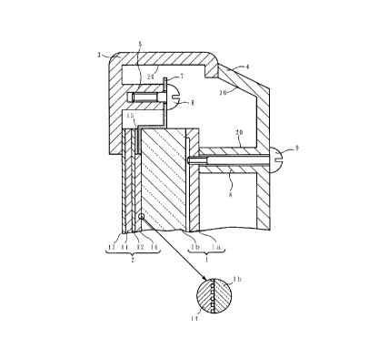
As shown in Fig. 7, the optical filter 2A comprises a filter
CA 02289565 1999-11-12
substrate 11A formed from reinforced glass, a transparent conductive
film 12A and an electrode 24 fixed on one surface (surface on the
side of PDP 1) of the filter substrate 11A, an anti-reflection film 26,
securely attached with transparent bonding agent 25 on the upper
surface of the transparent conductive film 12A and upper surface of
electrode 24, and an anti-reflection colored film 28 securely attached
with a bonding a~;ent 27 on the other surface of the filter substrate
11.
The filter substrate 11A is formed from a reinforced glass plate
of about 3mm thick (e.g., 3.2mm thick), which is first heated to about
600°C and then cooled by moving air for increasing strength and
made available as an economical and relatively lightweight substrate
of optical filter. The filter substrate 11A is not limited to that
manufactured by moving-air cooling process; it may be of chemically
reinforced glass, and its thickness is not necessarily limited to about
3mm.
The corners of the filter substrate 11A, each being formed
between its wider surface and side surface, are beveled to form
beveled surfaces llAa and llAa. These beveled surfaces are
provided to prevent the substrate 11A from being damaged by coming
into contact with other object during handling.
The electrode 24 is formed by printing a conductive metal (e.g.,
conductive paste). on peripheral portion of one surface of the filter
substrate 11A, while the transparent conductive film 12A is formed
by sputtering method covering almost all of one surface of the filter
substrate 11A not including the peripheral surface thereof, so that
the area covered by sputtering overlaps the internal peripheral
CA 02289565 1999-11-12
16
portion of the electrode 24 to be connected electrically therewith.
The transparent conductive film 12A is formed in a fashion similar to
that of the sputter film 12 as transparent conductive film of the first
embodiment. H~~wever, unlike the case of the first embodiment
wherein the transparent conductive film is formed on the PET film
12a, the thin silver films 12b and thin zinc oxide films 12c are
formed by sputtering method directly on one surface of the filter
substrate 11A as a mufti-layer film comprising thin silver films 12b
and thin zinc oxide films 12c which are laid alternately, as shown in
Fig. 4, so that a thin zinc oxide film becomes the top layer and to a
thickness (e.g., to about 100 ) with which a surface resistance of
about 2.6 S2 /cm2 can be obtained. When the surface resistance is
set to about Z.6 S2 /cmz, the amount of radiation of the
electromagnetic wave leaking outside from the PDP 1 can be
intercepted to the level or lower than the level required by safety
regulation or the like while maintaining required transmissivity
(e.g., 60%) for the visible rays as in the case of the first
embodiment.
The anti-reflection film 26 is an optical thin film comprising a
plurality of films formed on the surface of a transparent film by
vacuum evaporation method by using materials having different
refractive indexes, or is an optical thin film comprising a transparent
film and fluororesin film applied thereon, which is designed to
prevent the display light from PDP 1 or external light.
The anti-reflection colored film 28 comprises a fluorine-base
film containing F~igmenis serving as coloring matters for correcting
the colors developed by the PDP 1 and an optical thin film, similar to
CA 02289565 1999-11-12
17
the anti-reflection film 26, formed thereon for preventing the
reflection of the light. The peripheral portion of the anti-reflection
colored film 28 is beveled so that the beveled surface continues flush
with one of the beveled faces llAa of the filter substrate 11A so that
the film can be prevented from coming off during handling.
As shown in :Fig. 6, a conductive film 20 is formed on the inside
surface of the front portion 3A of the casing, inside surface of rear
portion 4A of the casing, surface of fixing boss 8 and the like,
whereby the transparent conductive film 12A of the optical filter 2A
is made to be connected with the metal portion la (grounding
portion) on the back of the PDP 1 through the grounding electrode 24,
fixing spring 21, nut 22, conductive boss 23 and conductive film 20
to discharge to the ground the electric charge induced in the
transparent conductive film 12A by the electromagnetic wave
radiated from the body lb of the PDP 1.
Then, as shown in Fig. 6 and Fig. 7, when the optical filter ZA is
installed in front of the PDP 1, the image light output from the PDP 1
passes through the optical filter 2A, and the electromagnetic wave
leaking from the PDP1 is intercepted by the optical filter 2A, while
the near-infrared ray radiated from the PDP 1 is cut off by the optical
filter 2A. According to the result of experiment, the intercepted
amount (attenuation) of electromagnetic wave is lOdB or more (dB,u
V/m) within frequency range of 30MHz - 130MHz. Therefore, when
combined with the electromagnetic wave intercepting ability of the
PDP 1 itself, the available intercepting ability is sufficient to clear
the level of leakage of electromagnetic wave allowed for the
information processing equipment under the requirements of the
CA 02289565 1999-11-12
18
Electrical Equipment Control Law, VCCI, FCC, EN and the like.
Further, for the visible rays and near-infrared ray, the optical filter
passes the visible rays having wavelength of 400nm - 700nm by about
60% and passes alr~out 10% (intercepting 90% or more) or less of near-
infrared ray haviing wavelength of 800nm - 1000nm. Therefore,
interference of the PDP with the operation of infrared-ray remote
control equipment or the communication equipment installed in the
vicinity can be prevented.
Further, the filter substrate 11A is formed from reinforced glass,
so that, when the optical filter 2A is installed in front of the PDP 1,
the warping and rc;sultant deflection of the filter substrate 11A due to
the heat given off for display by the PDP will not occur, and thus
degrading of the duality of displayed picture can be prevented.
Further, the filter substrate 11A is formed from reinforced glass,
and so its thickness can be made smaller than that of the filter
substrate formed from ordinary glass.
Further, the oeflection of the display light from the PDP 1 and
the external light are prevented by the anti-reflection film 26 and the
anti-reflection colored film 28 provided on both surfaces of the filter
substrate 11A respectively, whereby the decline of contrast is
prevented, and the colors developed by the PDP 1 are corrected for
easier maintenance of white balance and for preventing the broken
pieces of the PDP 1 from scattering around if it should be broken.
Next, the third embodiment of the invention will be described
referring to Fig. 8. In Fig. 8, for the parts common to those shown
in Fig. 6 and Fig. 7, the common reference numerals or symbols are
assigned so that duplication of the same descriptions can be avoided.
CA 02289565 1999-11-12
19
Fig. 8 shows an example of a large-size PDP device with an optical
filter. In Fig. 8'., numeral 1 denotes the PDP; 2B, the optical filter
for the PDP (hereinafter referred to simply as optical filter); 3A, the
front portion of the casing. The elastic portion of the fixing spring
21 is strongly pressed against the peripheral portion of the optical
filter 2B on the side of the PDP 1. The proximal end portion of the
fixing spring 21 is fastened to conductive boss 23 with the nut 22,
while the conductive bass 23 projects inside of the front portion 3A
of the casing, whereby the optical filter 2B is fixed to the front
portion 3A of the casing. A gap is formed between the PDP 1 and
the optical filter 2B.
The optical filter 2B comprises a filter substrate 11B, a
transparent conductive film 12A and an electrode 24 which are
securely attached on one surface (on the side of PDP 1) of the filter
substrate 2B, a transparent moisture-proof film 31 securely attached
with a transparent bonding agent 25 an the top surface of the
transparent conductive film 12A and that of the electrode 24, an
anti-reflection film 26 attached on the top surface of the moisture-
proof film 31 with the transparent bonding agent (not shown), a
moisture-proof sealing member 32 and a anti-reflection colored film
28 securely attached on the other surface of the reinforced filter
substrate 2B with a transparent bonding agent 27.
The filter substrate 11B is provided with bevels llBa and llBa,
which are similar to those of the second embodiment, while the
peripheral portion of t:he anti-reflection colored film 28 is also
provided with a bevel 28a continuing flush with one of the bevels
llBa. The moi~;ture-proof film 31 is formed from a transparent
CA 02289565 1999-11-12
airtight film such as the PET film and provided not only for covering
whole surface of the transparent conductive film 12A but also over-
lapping with the inside peripheral area of the grounding electrode 24
corresponding to the periphery of the transparent conductive film
12A.
The peripheral portions of the transparent bonding agent 25 and
the boundary edge between the moisture-proof film 31 and the
transparent bonding agent 25 are sealed with the sealing member 32,
whereby the transparent conductive film 12A (especially, thin silver
film) is prevented from being corroded by the water vapor in the
external air.
The inside surface of the front portion 3A of the casing, the
inside surface of the rear portion 4A of the casing (not shown in Fig.
8) and the surface. of fixing boss 8 (not shown in Fig. 8) are provided
with conductive film 20 by conductive film forming process, whereby
the transparent conductive film 12A of the optical filter 2B is
connected to the metal portion (for grounding) la (not shown) of the
back of the PDP 1 through the grounding electrode 24, fixing spring
21, nut 22, conductive boss 23 and conductive film 20 to discharge to
the ground the electric charge induced in the transparent conductive
film 12A by the electromagnetic wave radiated from the PDP1.
Then, as shown in Fig. 8, when the optical filter 2B is installed
in front of the 1'DP 1, the image light output from the PDP 1 is
transmitted by the optical filter 2B, and the electromagnetic wave
leaking from the PDP 1 is intercepted by the optical filter 2B, while
the near-infrared ray radiated from the PDP 1 is also cut off by the
optical filter 2B. According to the result of experiment, like the
CA 02289565 1999-11-12
21
case of the second embodiment, the intercepted amount (attenuation)
of the electromagnetic wave by the optical filter 2B is lOdB or more
(dB,u V/m) within frequency range of 30MHz - 130MHz.
Therefore, when combined with the electromagnetic wave
intercepting ability of the PDP 1 itself, the available
electromagnetic wave intercepting ability is large enough to clear
the leakage level limit of the electromagnetic wave required by the
Electric Equipment Control Law, VCC1, FCC, EN and the like.
Further, for the visible rays and near-infrared ray, like the case of
the first embodiment shown in Fig. 5, the transmissivity of the
visible rays having wavelength of 400nm - 700nm is about 60%, and
the transmissivity of near-infrared ray having wavelength of 800nm
- 1000nm is about 10% or less (intercepting 90% or more).
Therefore, the interference with the operation of nearby infrared-ray
remote control equipment or optical communication equipment by
the near-infrared ray can be prevented.
Further, all the surfaces of the transparent conductive film 12A
is covered with the moisture-proof film 31, so that, coupling with
sealing by the sealing member 32, the transparent conductive film
12A (especially, thin silver film) is prevented from being corroded
by the water vapor in the external air.
Further, the filter substrate 11B being formed from glass, the
filter substrate ll.B installed in front of the PDP 1 will not be warped
due to the heat given off for display by the PDP 1, so that the
degradation of the quality of displayed picture due to local warping
of the optical filter can be prevented.
Further, the anti-reflection film 26 and the anti-reflection
CA 02289565 1999-11-12
22
colored filter 28 provided on both surfaces of the filter substrate 11B
respectively prevent the reflection of the display light from the PDP
1 and external light, thereby preventing the decline of the contrast
and correcting the colors developed by the PDP 1 for easier
maintenance of white balance, while preventing broken pieces of the
filter substrate 11 B from scattering if it should be broken.
The second and the third embodiments are concerned with the
cases where a gap is provided between the optical filter 2A and the
PDP 1 and the optical filter 2B and the PDP 1, but the present
invention is not limited to these embodiments; for instance, the
invention is also applicable to the cases where the gap is not
provided between the optical filter 2A and the PDP 1 and between the
optical filter 2B and the PDP 1 like the case of the first embodiment.
Further, the invention is applicable to the case where the AN film
similar to that of the first embodiment is provided on the surface of
the optical filter ?A and on the surface of the optical filter 2B on the
side of the PDP 1.
In the above embodiment, the case where the display panel is a
PDP, but the present invention is not limited to such a case but also
applicable to display panels from which unnecessary electromagnetic
wave or near-infrared ray leaks.
INDUSTRIAL APPLICABILITY
As described in the foregoing, the optical filter for the display
panel according to the present invention is suited for being installed
in front of the display panel (e.g., PDP) of display device for
allowing the display light (visible rays) output from display panel to
CA 02289565 1999-11-12
23
pass and the electromagnetic wave leaking from display panel, to be
intercepted while suppressing the leakage level of the
electromagnetic v~rave to or below the leakage level limit required for
the information processing equipment and the like by the regulations
and preventing the interference with the operation of nearby remote
control equipment or communication equipment by the near-infrared
ray radiated from the display panel.