Note: Descriptions are shown in the official language in which they were submitted.
CA 02289736 2007-03-14
25679-44
-1-
METHOD AND DEVICE FOR MEASURING AN ELECTRICAL VOLTAGE
The invention concerns a method and a device for optical measurement of an
electrical voltage, preferably a high voltage.
Conventional voltage transformers used for measuring high voltages in power
technology installations are based on an inductive measurement principle;
capacitive
voltage dividers may also be used in addition. In conventional transformers,
expenditure on insulation increases at a disproportionately high rate in
relation to the
transmission voltage of the power supply network. Electromagnetic
compatibility
(EMC) has gained in importance in the course of increasing digitalization of
the
measuring technology following the transformers, wherein this measuring
technology
generally has lower interference thresholds than conventional analog
measurement
technology. Because of the inductive-capacitive coupling of the primary plane
(supply side) to the secondary plane (measurement and control side) in
conventional
voltage transformers, their use in connection with digital network technology
turns
out to be problematic as concerns EMC. Compared to conventional transformers,
little raw material is used owing to the small size of optical component
assemblies.
Optical transformers do not require any oil for insulation in principle, so
that the risk
of contamination of adjoining soil with oil in the event of a transformer
explosion due
to defects on the network side or device side is nonexistent.
Optical measuring methods in which electrical fields and electrical voltages
are measured via the Pockels effect in electro-optical crystals are already
generally
known from different references. In this connection, the physical properties
of an
electro-optical medium change as a function of the electrical field strength
in such a
way that the polarization state of the optical wave propagating through the
sensor
medium is influenced by a linear birefringence induced by the electrical
field. With
the help of an optical arrangement comprising a polarizer, a delay element, an
electro-optical material and an analyzer, in combination with electronic
evaluating
means, the measurement signal can be acquired for determining the electrical
voltage transverse or parallel to the propagation direction of the optical
wave. In
CA 02289736 1999-11-10
-2-
order to make it possible to separate the useful quantity - electrical voltage
- from the
interference quantities - damping along the optical signal path which is not
constant
over time, temperature dependE:ncies-on parameters of the optical components
employed - the optical signal path is divided into more than one partial beam.
The
partial beams are guided to separate receivers via different optical elements
and the
detected signals are, if necessary, subjected to digital signal processing
after
suitable processing through analog electronic means.
In DE 44 36 454 Al, polarized measurement light is guided through a Pockels
sensor device under the influence of the alternating field or AC voltage to a
beam
splitter which splits the optical wave into two different polarization planes.
The
method indicated in the embodiment form makes use of the transverse electro-
optical effect (Fig. 1) for measuring the electrical field. The method is
suitable for
measurement of voltages which drop transversely across the sensor crystal. It
is
possible to adapt the mc:asurenient range by changing the crystal length, but
the
maximum measurable voltage is limited by the electrical strength of the sensor
crystal. Due to the fact that the crystal dimensions are limited in practice,
the
measurement of high voltages by means of the transverse electro-optical effect
is
very uneconomical in technical respects; however, the measurement of "small"
voltages below the electrical strength of the crystal material through an
increase in
sensitivity by lengthening the crystal is useful.
DE 44 16 298 Al describes an embodiment form of the measurement
process and the device for carrying out the process which make use of the
longitudinal electro-optical effect. An electrical voltage to be measured
generates an
electrical fieldin the crystal whose flux lines run parallel to the
propagation direction
of the measurement light. Due to the maximum technically possible crystal
dimensions and the limited electrical strength in this connection, there is a
considerable increase iri expenditure on insulation for measurements of
electrical
voltages in the range of the maximum electrical strength of the arrangements.
DE 41 00 054 C2 proposes an optical measurement transducer which
supplies a measuremerit for electrical current by determining the magnetic
field and,
by means of an installeci capacitive divider, makes use of the voltage drop
across a
AMENDED SHEET
CA 02289736 1999-11-10
-3-
partial capacitance as a measurement for electrical voltage. The electrical
voltage is
exactly determined only when the indicated splitting ratio determined by
overvoltage
capacitance and undervoltage capacitance remains constant. Since a spatially
expanded undervoltage capacitance is used, the capacitance can be influenced
by
field distortion, so that the splitting ratio of the measurement transducer is
changed.
In general, constant field distributions cannot be assumed in practice.
DE 34 04 608 C2 describes a device for optical measurement of the electrical
field strength which supplies, via a transmission element, an optical wave of
a
sensor device for an electrical field which changes the degree of modulation
of the
optical wave depending on the electrical field strength. It is noted that the
utilized
sensor crystals exhibit a limited dependency of the optical effect on
temperature, but
there is no complete compensation of the temperature influence.
A device for measuring a voltage and an electrical field using light is
indicated
in DE 30 39 136 C2. Ttie paterit describes the use of a bismuth-germanium
oxide
crystal for voltage measurement and field measurement. It is indicated that
the
temperature dependencies of the material-specific constant can be assumed at
about 0.01 %/ K. Consequently, in a temperature range of AT=100K the error can
amount to 1%. For applications with higher accuracies, it is necessary to
compensate for the temperature characteristic not only of the sensor crystal,
but also
of the delay plate.
DE 28 45 625 Al describes an arrangement for electro-optical voltage
measurement which makes usE: of the longitudinal linear electro-optical effect
of a
piezoelectric fiber and in which there is effected an integration of the
optical effects
of the field strength distribution along the fibers by means of the spatial
dimensioning of the crystal fibers. According to the state of the art, a
crystal fiber of
this type is not currently commercially available, so that this method of
voltage
measurement has not been successful in practice in technical respects relating
to
large-series manufacture.
DE 21 31 224 C3 discloses a device for measurement of voltages at high-
voltage conductors in which it is indicated that the electrical field
proportional to the
voltage to be measurecl changes the polarization plane of polarized light
which is
AMENDED SHEET
CA 02289736 1999-11-10
-4-
coupled into a light waveguide. In a suggested arrangement, the light
waveguide is
guided along a curvy path in ornder to increase the effect. A high temperature
dependency of the measurement signal caused by the linear birefringence of the
light waveguide induceci by beriding would be expected in this embodiment.
DE 15 91 976 A 11 describes an electro-optical voltage reducing device and its
application for measuririg voltages. In this case, the polarization of a light
bundle
traversing a quantity of electro-optical cells which are electrically
connected in series
is changed and read out by a P'ockels cell via a compensating circuit. In
principle,
the described arrangerrient is a resistive-capacitive splitter whose voltage
drops
across partial capacitarices are read out optically. The method has the
disadvantage that temperature dependencies of the optical elements are not
compensated and that the suggested device is uneconomical in technical
respects
and is accordingly expe!nsive tci produce because the cost of the voltage
divider is
added to that of the optical construction. Further, the compensation circuit
necessitates supply of a secondary electrical voltage.
DE 44 36 181 A'1 discloses a method and a device for measuring an electrical
AC quantity with temperature compensation through fitting. A suggested scaling
circuit takes the ratio of'AC signal component to DC signal component of the
intensity signal of the optical wave detected by the receivers. A divider is
used to
carry out this function. No steps are indicated for suppressing the effects of
tolerances of the structural component parts in the scaling stage.
Therefore, it is the object of the invention to provide a method and a device
for measuring an electrical AC voltage by means of the electro-optical effect
in which
the measurement can be carried out under open-air conditions also in the high-
voltage and very high-voltage planes in a technically simple manner.
This object is mE:t in the method according to the generic part in that a
measurement path coniprehends a substantial portion of a path along which the
measured voltage U drops, wherein the measurement path is represented by
sensor
crystals whose quantity and arrangement allow substantial detection of an
inhomogeneous electrical field distribution in order to determine in a highly
accurate
manner from the individual field strength values by integration over the
AMENDED SHEET
CA 02289736 1999-11-10
-5-
measurement path a measurenient U' proportional to the total voltage U to be
determined.
The sensor element contains at least one active sensor part. The voltage
present at the sensor element clrops at a quantity NsA,, (NSA is greater than
or equal
to 1) of active sensor parts, so that the partial voltage(s) USA,,..USA,NSA
dropping at the
active sensor part(s) is (are) measured and available for further processing.
A
quantity NSE (NSE is greater thari or equal to 1) of sensor elements is used,
so that
the sum of the partial voltages IJsE,,==UsE,NSE dropping at them is available
and is
used for determining the total voltage to be measured. The partial voltages
UsE,,==USA,NSA are again composed of a sum of partial voltages USA,==USA,NSA=
Measurement light generated by a light source penetrates an active sensor
part comprising at least two serisor crystals at which an electrical voltage
drops.
After the measurement light has traversed the sensor crystals, its
polarization state
is further used for processing information which, after suitable evaluation,
represents
a measurement for the electrical voltage dropping over the sensor crystals,
wherein
the selected quantity N,;K of serisor crystals on the measurement path is
sufficiently
large with respect to the inhomogeneity of the electrical field distribution
and the
length of the measurerrient path is in the same order of magnitude as the
length of
the path along which the voltage to be measured drops.
The active sensor part contains at least one optical element made from a
material with temperature-dependent optical activity. The temperature-
dependency
of the optical activity is made available as a measurement for the temperature
prevailing at the temperature-dependent optical element to assess the
measurement
values. The active sensor part is constructed in such a way that the sensor
crystals
contained therein are penetrated by an individual light beam one after the
other in
the same crystallographic orieritation, the results of the electro-optical
effects in the
individual crystals are summed, and the sum values are available as a basis
for
determining the voltage present at the active sensor part and are applied for
this
purpose. The active sE:nsor part has a carrier which serves to hold and align
the
crystals that are used.
AMENDED SHEET
CA 02289736 1999-11-10
-6-
The optical waves transniitted by the active sensor parts are detected and, as
signal I, are each converted to a scaled signal 'N via a component assembly
contained in evaluating means intended for this purpose. The detected signal I
has
an AC component IAc as characteristic quantity which changes over time with
the
frequency of the voltage to be nieasured, whose time constant is designated by
TAC.
The change in a DC cornponeni: 'DC is described as another characteristic
quantity of
the detected signal I with time constant TDC, wherein time constant TpC is
appreciably
greater than TAc and the: scaling is effected by multiplying the detected
signal I by a
factor K in such a way ttiat the [)C component of the scaled signal 'N takes
on the
predetermined value of .a reference signal Vref, and factor K which is used in
preparation is determinE:d in a closed control loop. Instead of the DC
component,
the peak value can also be detected and used further.
A suitable device for measuring an electrical AC voltage has at least one
light
source, at least one optical transmission path, at least one active sensor
part and
evaluating means makirig use of the Pockels effect. The active sensor part has
at
least two electro-optical sensor crystals which are penetrated by a polarized
measurement light, wherein a temperature-dependent optical element can follow
the
sensor crystals. The cristals penetrated by a polarized measurement light and
the
temperature-dependent optical element preferably comprise Bi4Ge3O12, Bi4Si3O12
or
B12GeO20, Bi1zSiO20 or combinations of crystal group 43m or 23.
The active sensor part comprises a plurality of sensor crystals which are
directed successively, can be penetrated by an individual light beam, have the
same
crystallographic orientation and are arranged in or at an appropriate carrier
so as to
be adjustable for orientation relative to one another in the direction of the
light
radiating through them. These sensor crystals are preferably axially aligned.
The sensor element contains a device which makes it possible to arrange one
or more active sensor parts in such a way that the voltage present at the
sensor
element drops in partial voltages at the active sensor part(s) and the sum of
the
partial voltages equals 1:he applied voltage. Sensor elements can be combined
by
holding elements and field-control elements in such a way that the voltage
applied
thereto drops at the indlividual sensor elements in partial voltages.
AMENDED SHEET
CA 02289736 1999-11-10
-7-
The device contaiins, as evaluating means, at least one component assembly
by means of which the scaling of the detected signal I is carried out by
multiplying
the input signal by a factor which is generated by a function unit whose input
quantity represents the difference between a reference signal and the factored
input
signal. An integrator, a low-pass filter or a peak value rectifier can
advantageously
be used as a function unit.
The advantages of the invention consist in that the device according to the
invention has a modular construction, so that the device is to be adapted for
voltage
measurement in differerit voltagie planes without the need for basic design
changes.
An economical voltage transformer can be realized by means of this step by
increasing the piece nurnber of an active sensor part.
A further advantage of the invention consists in that the discrete summing of
the electrical field strength for approximating the applied electrical voltage
is carried
out by using a large nurnber of sensor crystals. Accordingly, the use of long
crystal
rods to which the voltage to be measured is applied can be dispensed with.
Therefore, a reduction in costs can be expected because of the smaller crystal
volumes. The use of a temperature-dependent optical element as a temperature
sensor makes it possible to compensate for temperature-dependent effects.
A control loop is proposed in the scaling stage of the evaluating circuit for
carrying out scaling; this control loop regulates structural component part
tolerances
through the use of feedback, in contrast to methods without feedback. This
control
loop can advantageously control subsequent analog and digital circuits.
A further advantage of the solution according to the invention consists in
that
a discrete voTtage divider for controliing the voltage drop in the suggested
optical
transducer is not needE:d. The electrical voltage is determined in accordance
with its
definition by integrating the electrical field strength components on the
measurement
path.
AMENDED SHEET
CA 02289736 2008-04-01
25679-44
-7a-
According to one aspect, the invention provides a
method for measuring an electrical voltage, wherein the
electrical voltage is an alternating quantity, making use of
at least one sensor element and evaluating means by
utilizing the Pockels effect and using at least one light
source and at least one optical transmission path, wherein a
measurement light generated by the light source penetrates
an active sensor part comprising at least two sensor
crystals at which an electrical voltage drops, and, after
the measurement light has traversed the sensor crystals, the
polarization state of the measurement light is further used
for processing information which, after suitable evaluation,
represents a measurement for the electrical voltage dropping
over the sensor crystals, wherein the selected quantity of
sensor crystals on the measurement path is sufficiently
large with respect to the inhomogeneity of the electrical
field distribution, and the length of the measurement path
is in the same order of magnitude as the length of the path
along which the voltage to be measured drops, wherein the
evaluating means is used with a corresponding component
assembly by means of which scaling is carried out by
multiplying an input signal by a factor which is generated
by a function unit, its input quantity representing the
difference between a reference signal and a factored output
signal, and wherein the function unit provides integration.
According to a further aspect, the invention
provides a device for measuring electrical voltage, wherein
the electrical voltage is an alternating quantity, and with
at least one light source and at least one optical
transmission path, at least one sensor element and
evaluating means accompanied by the use of the Pockels
effect, wherein the at least one sensor element contain at
least one active sensor part comprising at least NSK (NSK is
CA 02289736 2008-04-01
25679-44
-7b-
greater than or equal to zero) electro-optical sensor
crystals (SK1 ... SKN) which is penetrated by a polarized
measurement light, wherein the evaluating means contain at
least one component assembly by means of which scaling is
carried out by multiplying an input signal by a factor which
is generated by a function unit, its input quantity
representing the difference between a reference signal and a
factored input signal, and wherein the function unit is an
integrator.
CA 02289736 1999-11-10
-8-
The invention will be described more fully in the following in an embodiment
example. Shown in the accompanying drawings are:
Fig. 1 the principle of a F'ockels cell based on the transverse electro-
optical
effect;
Fig. 2 principle of a Pockels cell based on the longitudinal electro-optical
effect;
Fig. 3 principle o-f an expanded Pockels cell for voltage measurement and
temperature detection;
Fig. 4 use of a plurality of sensor crystals for voltage measurement;
Fig. 5 basic construction of the device for measuring a voltage;
Fig. 6 basic modular construction of the device for adapting the voltage
plane;
Fig. 7 basic construction of the evaluating means;
Fig. 8 conventional scaling of an optical signal by means of dividers;
Fig. 9 scaling of the optical signal by means of regulated multiplier.
As is known, the measurement of the electrical field can be carried out with a
Pockels cell. Figs. 1 and 2 show the basic construction of a Pockels cell. A
light
source 31 emits an optical wave which is guided via a polarizer 11, an electro-
optical
element 12, a delay element 13 and an analyzer 14, to an optoelectronic
transducer
32. When a crystal without natural linear birefringence is used as electro-
optical
element 12, the operating point of the arrangement should be set at a delay of
a
quarter wavelength to ensure niaximum sensitivity and linearity through the
use of a
CA 02289736 1999-11-10
-9-
delay plate 13. When the transverse electro-optical effect is used (Fig. 1),
the light
propagation direction and the modulating electrical field are perpendicular to
one
another. In order to ma'ke use of the longitudinal electro-optical effect
(Fig. 2,
electrical field and light propagation direction extend parallel to one
another), the
electro-optical crystal 11. is orierited in such a way that the coupled-in
linearly
polarized optical wave propagates along a main axis in the sensor crystal 12
and the
polarization plane of the: optical wave is oriented at a 45-degree angle to
the other
electro-optically characterized axes of the crystal in the presence of field
E. The
analyzer 14 converts the optical signal which is phase-modulated by the
present
electrical field into an intensity-modulated signal. It is possible to
determine the field
strength E from the intensity-modulated signal made available by the receiver
32 via
evaluating means.
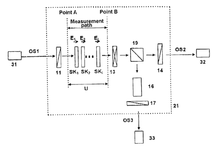
Fig. 3 shows the principle of the expanded Pockels cell used in the invention.
In contrast to Figs. 1 and 2, this Pockels cell comprises a plurality of
sensor crystals
SK; (where i= 1,2..NsK, NSK is greater than or equal to zero) and comprises,
in
addition, a beam splitter 19, a temperature-dependent element 16, an analyzer
17
and a receiver 33. The connection of the light source 31 to the active sensor
part 21
represents the optical transmission path OS1, the connections from 21 to the
electro-optical transducers 32 and 33 are realized by means of the optical
transmission paths OS2 and 0S3, respectively. The optical wave is modulated by
the active sensor part 21 at discrete locations of the sensor crystals SK;
through the
locally prevailing field s'trength E,. After traversing the beam splitter 19,
one partial
wave is supplied via a temperature-dependent optical element 16 to an analyzer
17
and a receiver 33. The other partial wave directly strikes the analyzer 14 and
a
receiver 32 after the beam splitter. When the Pockels cell works according to
the
longitudinal electro-optical effect, the individual modulations add up at the
sensor
crystals when the latter are arranged in the same crystallographic
orientation. The
sum of individual modulations results in a total phase delay F of two
orthogonal
partial waves.
The voltage to be deterrnined drops on the measurement path of the active
sensor part between points A and B. The associated assumed field strength
curve
(solid line) is shown in Fig. 4 as a function of the measurement point.
According to
CA 02289736 1999-11-10
-10-
the definition for determining thE: voltage between points A and B, the
integral of the
field strength path product uses:
a
UAB = fEdT (1)
A
When the field strength curve is approximated by a step function with a
quantity of
NSK steps, UA,B changes to:
NSK
UA,B Ef ' dt ~ (2)
i=1
where E; represents the constarit field strength at the sensor crystal SK; at
step i with
width d;. The transition i-rom equation (1) to equation (2) is possible on
condition that
exclusively the field strength cornponent E in path direction dl has an
influence on
the value of the integral. If the widths of steps d; are identical to a
constant d and
the lengths I; of the sensor crystals are likewise equal to a constant I,
equation (2)
results, by expansion, iri equation (3):
NSK
UA,B = a Et = 1 (3)
1 i=1
When the longitudinal electro-optical effect is used, the phase delay of two
orthogonal optical partial waves is proportional to E; and I; (see A. Yariv,
P. Yeh,
"Optical Waves in Crystals"):
Pt Et = 11 (4.1)
so that, in combination with equation (3), UA.B is proportional to the sum of
the partial
phase delays:
UA,Ba~ri (4.2)
CA 02289736 1999-11-10
-11-
When the partial phase delays brought about by the individual sensor crystals
are
summed according to the following equation:
r = ~ rf (5)
the total phase delay Faccording to equations (4.2) and (5) is proportional to
the
voltage UA B to be measijred.
Therefore, with a sufficiently large quantity of sensor crystals, the
determination of the electrical voltage by calculation of the path integral of
the
electrical field strength can be traced to a summing of discrete field
strength path
products. The more sensor crystals are used, the more exactly the summing
approximates the integral. However, this also results in increased cost for
the
crystals and increased loss caused by surface reflections. In practice, costs
and
measuring accuracy are to be optimized.
The second optical wave coupled out by the beam splitter traverses a
temperature-dependent optical element which is optically active. By means of
this
arrangement, a correction factor can be obtained which compensates for the
temperature-dependent: errors of the linear birefringence in the sensor
crystals and
in the delay plate.
Fig. 5 shows the schematic construction of the device for measuring voltage
comprising light sources and evaluating means 30 and a sensor element 20 which
comprises a quantity N,A of active sensor parts 21-X and holding and field
control
elements 22. The optical transmission paths between the sensor element 20 and
evaluating device 30 are designated inclusively by OS. Optical waves are
supplied
to the optical sensor element along the transmission path OS. At least two
optical
waves are guided back from the sensor element 20 to the evaluating means 30
via
the transmission path OS. The, evaluating means generate a measurement U' for
the sum of the voltages Usa,,..Usa,r,sA present at the active sensor parts 21-
1..21-NsA.
The voltage U' is proportional to the total voltage U.
Fig. 6 shows an example for the modular construction for adapting the voltage
plane when each of the sensor' elements 20-X (X=1,2..NSE) contains exactly one
active sensor part 21, so that NSE is equal to NSA in this case. The sensor
elements
CA 02289736 1999-11-10
-12-
20-X are arranged in such a way that the partial voltages U,', U2',...UNSE' of
the
sensor elements deterrriined in the evaluating means 30-X give a measurement
U'
proportional to the total system voltage U by summing in unit 35. Unit 35 can
be part
of the evaluating means 30 or a unit composed of 30.
In this embodiment exarriple, Bi4Ge3O12, belonging to class 43m of the cubic
crystal system, will be considered as sensor crystal. The crystal has no
natural
linear birefringence and is not optically active. Due to the absence of
optical activity,
a large number of sensor crystals of the same kind can be arranged one behind
the
other in a simple mannE:r as regards construction, so that the effects of the
longitudinal Pockels effect are summed in the form of induced linear
birefringence in
the individual crystals F; to form a total phase delay F of the propagating
orthogonal
partial waves. When thle polarizer 11 in Fig. 3 is oriented at an angle of 45
to the
electro-optically characterized axes of the sensor crystals, all of which have
the
same orientation, and the analyzer 14 is arranged so as to be crossed with the
input
polarizer, the intensity I., can be detected at the receiver 32 according to
the
following equation:
Il = IlDc (1 + sin(6),
where F is the phase delay due to the Pockels effect between the optical
partial
waves that are polarizeld along the first and second electro-optically
characterized
axes and the light propagation 'takes place in the direction of the third
electro-
optically characterized axis. Thie DC component of the intensity I, detected
at the
receiver is designated by I,,oC. The value F can be calculated from the sum of
the
partial phase delays F; at the individual sensor crystals, wherein NSK shows
the
quantity of sensor crystals use<i.
NSK
r = E r, (7)
~=1
CA 02289736 1999-11-10
-13-
According to the longitudinal electro-optical effect, the partial phase delays
f;
of the individual sensor crystals gives:
2TL 3
rt __ T no = r41 = E r = li (8)
0
where: no is the index of refraction,
Ao is the wavelength of the optical wave,
r41 is the electro-optical constant,
EZ.; is the eIectrical field component in the propagation direction of the
optical wave in crystal i,
I; is the length of the light path in the electro-optical crystal.
The second parti,al beam in Fig. 3 is guided via a temperature-dependent
optical element 16 and via an analyzer 17 to a receiver 33. When Bi12GeO20,
for
example, is used as terriperature-dependent optical element 16, a measurement
can
be determined for the temperature by making use of the temperature dependency
of
the natural optical activity. For -this purpose, the polarization plane of a
continuous
optical wave is rotated by A6 during a change in temperature of T. The scaled
optical intensity 12 can be detected at the receiver 33 with the DC component
I2,oc
according to:
12 = 12.DC(1 + sin(I') - sin(2 = 0)) , (9)
wherein the angle 6 is composed of the rotation of the polarization plane by
the
optical activity at reference temperature 6o and the proportion 08 caused by
changes in temperaturE:.
0 = eo+ne (10)
The analyzer is oriented by an angle of 45 + 06max to the angle 60. Due to
the
additional rotation by A6max, the change of A6 within the interval [-A6max 1+
Aemaxl
always leads to a modulation of the output signal 12 without a change in sign.
CA 02289736 1999-11-10
-14-
In order to compensate for damping influences on the optical transmission
path between the light source and the receiver, it is advantageous when the
signals
I, and 12 are divided into the DC component and AC component and scaling is
carried out as prescribed by the following equations:
I~ = ~1Ac^ = siII~li J (1 1 )
1, D7
I2N = ~2,AC = sin(T') =sin(2 = (A e + 0e,~)) (12)
z,,D~7
In the equations shown above, fis an AC signal in the frequency range of
20Hz to 20kHz; on the other hand, A6 changes only "slowly" in the range of the
thermal time constant of the measuring device in the frequency range below
20Hz.
Integrating signals I1N and 12N over a time interval T with respect to amount
(T
should be appreciably less than the thermal time constant and appreciably
greater
than the period of the lower bouindary frequency of the AC signal F) and
dividing
them gives the quantity T21 according to the following equation:
tO+T
,r 16 idt
T21 = t_:to =Sin(ne + oe.) (13)
to+s
f IIlxldt
t ==to
For changes of Ci6 + L1ernaX << 1, the sine function can be approximated
linearly by its argument. Equation (13) gives:
De = T21 Ae,,,,x (14)
It is possible to cletermine temperature by means of A6 because Ae changes
approximately linearly ciepending on the temperature and an inverse function
can be
CA 02289736 1999-11-10
-15-
determined in a matherriatically definite manner in the interval in question.
It is
possible to correct the temperature characteristic of the signal by means of
this
determined measurement for the change in temperature with respect to the
reference temperature. An output signal A which can be corrected by factor KT
for
temperature compensation is obtained by forming the arc sine of I1N. The
factor KT
must be known by mearis of calibration.
A = KT- a sin(IIN) (15)
The signal A is accordingly proportional to the total phase delay F of the
sensor element and to the sum of the electrical field strengths prevailing at
the
measurement locations.
A precondition of the indicated process is that exclusively the electrical
field
strength component in the path direction has an influence on the value of the
integral from (1) in the transitiori from the defining equation of the
electrical voltage
(1) to equation (2). When the direction of light propagation in the sensor
crystal is
selected parallel to the directiori of the integration path and the measured
light
propagates along an optical main axis in the sensor crystal, then, when a
cubic
crystal is used, only the electrical field component has an influence on the
sum in
equation (2) which is dii-ected parallel to the propagation direction of the
measurement light. In order to show this, the indicatrix is used as a
descriptive
model of the index of re.fraction depending on the light propagation
direction. The
mathematical formulation of the indicatrix (see A. Yariv, P. Yeh, "Optical
Waves in
Crystals") gives:
12(x2+y2+z2)+2r41=(Ex -y -z +Ey -z -x +Ez =x =y)=1 (16)
no
where direction x is corisistent with crystal direction <100>, y is consistent
with
<010> and z is consistent with <001>. With consideration to the light
propagation in
CA 02289736 1999-11-10
-16-
direction z, a section of ithe indicatrix in the x-y plane is carried out in
the coordinate
origin, which can be described rnathematically by the condition z=O.
In this case, the indicatrix changes to
12(x2+y2)+2r41=EZ =x =y=1 (17)
no
After carrying out a coordinate transformation from (x, y) to (x', y') with
x = (x'-y) (18)
V12-
y = (x' +y) 1 V12- (19)
the indicatrix from (17) can be clescribed by
,2 12
2 + y 2 = 1 , (20)
nx, ny,
with the refraction indexes nX, and nY, along the x' direction and y'
direction (ignoring
terms with higher powers of r41) according to
nX, = n 0 - 2 n 3r41Ez (21)
ny, = no +~ n 3 r41 E. (22)
CA 02289736 2007-03-14
25679-44
-17-
It is shown in (21) and (22) that in the case of light
propagation in the z-direction along a main axis in the
crystal the indicatrix is influenced exclusively by the
electrical field component in the propagation direction. In
this case, other field components do not influence the
indicatrix and accordingly the phase delay, which is
proportional to the difference of nX, and nY,, as measurement
for the local field strengths.
Accordingly, the signal A from (15) is
proportional to the voltage UA,B which drops over the sensor
crystals which are located on the measurement path of the
active sensor part 21.
When the total voltage drop is distributed over a
plurality of sensor elements (Fig. 6) in order to adapt the
voltage plane, the summing of the partial voltages of the
sensor elements leads again to the total voltage.
If the sensor element contains only one individual
sensor crystal, no voltage is measured in this case, but
only a field strength component which drops over the sensor
crystal. The voltage sensor can be used as a sensor for an
electrical field strength component.
Fig. 7 shows the evaluating means 30. They
contain a light source 31 and at least two electro-optical
transducers 32 and 33. The signals are pre-processed by
component assemblies 40, digitized by a multi-channel
A-D converter 51, processed in a computer 53 and made
available as output quantity A via a D-A converter 52. The
signal detected by receivers 32 and 33 is scaled in
component assemblies 40, so that the following A-D converter
is adequately controlled. For this purpose, an analog
divider DIV and an analog high-pass HP and low-pass LP
CA 02289736 2008-04-01
25679-44
-17a-
which realizes the mathematical function directly as is
shown by way of example in Fig. 8 are usually used. As
illustrated in Fig. 8 the output of the high-pass HP is the
IAC and the output of the low-pass TP is the DC current IDC.
.5 The scaling is usually used in the case of optical sensors
which transmit, on an optical transmission path, an
intensity-modulated signal undergoing a temporal change in
optical damping. Further, the influence of the steepness of
the receiver can also be eliminated. The circuit that is
usually used has the disadvantage that the divider (DIV) is
no longer adequately controlled when there is an increase in
damping on the optical transmission path between the light
source and receiver or, on the other hand, can be
overcontrolled when there is a decrease in damping on the
optical transmission
CA 02289736 2007-03-14
25679-44
-18-
path. Therefore, errors can occur as a result of the electronics. A solution
to this
problem is offered by the use of a multiplier which is integrated in a
feedback loop,
so that tolerances of the structural component parts can be compensated by the
control loop. It is necessary to compensate for tolerances because, in
practice,
there are no commercially available structural component parts which have a
sufficient accuracy.
A basic construction of the circuit is shown in Fig, 9. The input signal I to
be
scaled is fed to a multiplier MUL as first factor, the second factor for the
multiplier is
obtained by the function unit INT from the output signal of the multiplier MUL
and
from a reference quantity Vfef. In one embodiment example, the function uuit.
can be
an integrator. In this case, the integrator generates a controlling variable K
as a
second factor for the multiplier which regulates the DC component of the
output
quantity to the value predetermined by Vref. The AC component of the signal I
is
scaled by the same factor determined by the regulation for the DC component.
In
another embodiment form, the function unit INT can be a peak value rectifier.
In this
case, the input signal would be scaled by a factor so that the peak value of
IN
corresponds to the level Vref. The multiplier can also be realized by another
voltage-
controlled coefficient element.