Note: Descriptions are shown in the official language in which they were submitted.
CA 02289935 1999-11-10
Case 1526
VOLTAGE REGULATOR CIRCUIT FOR SUPPRESSING LATCH-UP
The present invention concerns a voltage regulator circuit for
regulating a voltage disturbed by a phenomenon known as « latch-up ».
Numerous voltage regulator circuits exist in the prior art.
A circuit of this type is disclosed in GB Patent No. 2 298 939, and is
shown in Figure 'I A of the present description. This circuit includes a
control
transistor Q1 connected in series between an input terminal I and an output
terminal O, and <in output voltage detector D formed of two resistors Ra
and Rb connected in series between output terminal O and the circuit's earth.
A voltage corresponding to the output voltage detected by detector D
is compared to a reference voltage E3 by an operational amplifier AO, and
the output voltage thereof is applied to the base terminal of a transistor Q2.
Thus a base current of control transistor Q1 can be controlled by the output
voltage of operational amplifier AO, via transistor 02, so that the impedance
of control transisi:or Q1 is controlled so as to provide a predetermined
voltage at output terminal O.
One problem encountered during the operation of such a circuit lies in
the unintentional appearance of phenomena known as « latch-up » which
occur in an electronic component of the circuit, following external
disturbances such as the supply of an electric voltage, an electric current or
radiation.
« Latch-up » is commonly used to designate any phenomenon
occurring in an integrated circuit following external disturbances such as the
supply of an electric voltage, an electric current or radiation.
Numerous devices exist in the prior art for detecting « latch-up » in a
substrate and, in particular, devices analysing a current capable of being
disturbed by said phenomenon.
A device of this type is disclosed in Japanese Patent Application No. 5
326 825 in the narne of FUNAI ELECTRIC CO LTD, and is shown in Figure 1 B of
the present description. This device includes an integrated circuit IC1 at a
first
terminal of which is provided a supply voltage Vdd, via a bipolar transistor
T1, and at the second terminal of which is connected a resonant circuit
formed of a resistor R3 .and a capacitor C3. A detection integrated circuit
IC2 includes an earth terminal, a first terminal at which is provided supply
voltage Vdd, and a second terminal connected to said resonant circuit as well
as to the base terminal of a bipolar transistor T2 via a resistor R2. The base
CA 02289935 1999-11-10
-2-
terminal of transistor T1 is connected to the collector terminal of transistor
T2 via a resistor R1, and the emitter terminal of transistor T2 is earthed.
In the devi~~e described hereinbefore in relation to Figure 1 B, if latch-up
occurs, a significant drop in supply voltage Vdd is detected by integrated
circuit IC2. In this case, transistors T1 and T2 are blocked, and the voltage
supplying integrated circuit IC1 is interrupted, which initialises the
circuit.
Subsequently, integrated circuit IC1 again operates normally.
However, these devices have complex structures and require a large
number of electronic components to perform the detection and regulator
functions.
One object of the present invention is to provide a voltage regulator
circuit intended to suppress any inadvertent latch-up phenomenon.
Another object of i:he present invention is to provide a circuit of this
type which answE~rs criteria as to cost and simplicity.
i 5 These objects, in addition to others are achieved by the voltage
regulator circuit a:ccordin~~ to claim 1.
One advantage of the circuit according to the present invention is that
it provides a voltage regulator circuit having a structure not very complex
which makes it cheap.
Another advantage of the circuit according to the present invention is
that it provides a circuit including voltage comparison means to the input of
which is supplied the regulated voltage, these means being arranged so as to
define two voltage thresholds capable of being predetermined to respond to
the needs of the user.
These objects, features and advantages of the present invention, in
addition to others will appear more clearly upon reading the detailed
description of a preferred embodiment of the invention, given solely by way
of example, with reference to the annexed drawings in which:
- Figures 1 ~4 and 1 B which have already been cited show two voltage
regulator circuits according to the prior art;
- Figure 2 :shows a preferred embodiment of a voltage regulator circuit
according to the present invention;
- Figure 3 shows in detail the preferred embodiment of the detection
means of the circuit of Figure 2;
CA 02289935 1999-11-10
-3-
- Figure 4 :>hows the relationship between three voltages present in the
voltage regulator circuit according to the preferred embodiment of the
present invention; and
- Figures 5~4 and 5B show timing diagrams of the regulated voltage
and the signal supplied by the voltage regulator circuit according to the
preferred embodirnent of the present invention.
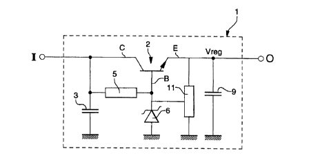
Figure 2 snows a preferred embodiment of a circuit 1 according to the
present invention.
Circuit 1 in<;ludes an input terminal I and an output terminal O from
which a regulated voltage Vreg has to be supplied, voltage Vreg being
supplied so as to be substantially equal to a voltage level Vo. Circuit 1
further
includes a bipolar transisi:or 2, two capacitors 3 and 9, a resistor 5, a
Zener
diode 6, and voltage detection means 11.
Bipolar transistor 2 typically includes a collector terminal C, an emitter
terminal E and a vase terminal B, terminals C and E being respectively
connected to terminals I a.nd O. Resistor 5 is connected between terminal B
and terminal C of transisi:or 2.
Zener diodE: 6 is arranged so as to supply a voltage having a value
selected so as to form voltage level Vo at output terminal O.
Capacitors 3 and 9 are connected across input terminal I and earth,
and across output terminal O and earth respectively. Those skilled in the art
will note that capacitor 3 is conventionally used as an interference
suppression capacitor, and that capacitor 9 is conventionally used as a
smoothing and/or interference suppression capacitor. Capacitor 3 is used
only by way of im~~rovement in the present invention has thus not limiting
character with respect to the present invention.
Means 11 include an input terminal connected to terminal O, so as to
receive at its input voltage Vreg, an earth terminal, and an its output
terminal
connected to terminal B, so as to supply at output a control voltage Vres to
control transistor 2. Means 11 are arranged so that they detect whether
voltage Vreg is di;~turbed by latch-up and, if necessary, command
initialisation
of this voltage at its initial voltage level Vo, as is explained in more
detail
hereinafter.
Following numerous experiments, the Applicant of the present invention
has established that one of the most efficient solutions for suppressing latch-
up in an integrates circuit consists in bringing the level of the supply
voltage
of the integrated ~~ircuit disturbed by said phenomenon to the earth
potential,
CA 02289935 1999-11-10
-4-
for a sufficient period of time for the circuit to drop below a certain
voltage
threshold.
For this purpose i:he voltage regulator circuit of the present invention
comprises voltage detection means which, following a "latch up" type
disturbance, bring the regulated voltage to the earth potential, thereby
eliminating this disturbance.
Figure 3 shows in detail the preferred embodiment of means 11,
according to the present invention.
Means 11 include:> reference voltage supply means 20 for supplying a
reference voltage Vref from voltage Vreg, a voltage divider 21 intended to
supply two corrected regulated voltages Vreg' and Vreg" from regulated
voltage Vreg, two voltage comparators 23 and 22 for comparing voltage
Vref to voltages Vreg' and Vreg" respectively, and control means 24 for
supplying, if necE;ssary, voltage Vres capable of controlling transistor 2,
and
regulating voltagE~ Vreg.
Means 20 include an input terminal connected to the input terminal of
means 11 (i.e. to terminal O), so that means 20 receive at its input voltage
Vreg, an earth terminal connected to earth, and an output terminal
connected to comparators 22 and 23, so that means 20 supply at its output
voltage Vref. Means 20 are known in the art, see for example the articles
« CMOS Analog Integrated Circuits Based on Weak Inversion Operation », by
E. Vittoz et al, IEEE Journal of Solid States Circuits, vol. SC-12, No. 3,
June
1977, and « CMC~S Voltage References Using Lateral Bipolar Transistors »,
by M. Degrauwe et al, IEE=E Journal of Solid States Circuits, vol. SC-20, No
6,
December 1985.
The operation of these means will be recalled briefly with reference to
Figure 4. Figure ~l shows a curve 31 corresponding to the relationship
between voltage Vref and voltage Vreg. In this example, means 20 are
arranged so that, for a value of input voltage Vreg greater than 1.5 V,
output voltage Vref is substantially equal to a voltage threshold Vr' of the
order of 1.2 V, and there exists a voltage level across which voltage Vref is
substantially equal to a voltage threshold Vr", for low values of voltage
Vreg.
A first voltage level A'Vr' is defined as the voltage level below which a
latch-up phenomenon is assumed to occur. In other words, when voltage
Vreg drops significantly, a latch-up phenomenon is assumed to be responsible
for this drop, as Noon as voltage Vreg becomes lower than A'Vr'. A second
voltage level A"Vr" is also defined as the voltage level below which a latch-
up
CA 02289935 1999-11-10
-5-
phenomenon is suppressed. In other words, when there is a drop in voltage
Vreg, as is the case when a latch-up phenomenon occurs, this disturbance is
suppressed, as soon as voltage Vreg becomes less than A"Vr". Voltage
levels A'Vr' and A"Vr" are predetermined values according to the particular
specificity of the user's requirements.
In the preferred ernbodiment shown in Figure 3, voltage divider 21 is
formed by a resistive bridge formed of three resistors 25, 26 and 27
mounted in series between output terminal O and earth. The point of
connection between the two resistors 26 and 27 is connected to a first input
of comparator 2~~, so as to provide voltage Vreg' at its input. This voltage
is, by definition, proportional to voltage Vreg, the ratio of proportionality,
referenced A', being predetermined and dependent upon the values of
resistors 27, 26 and 25. By way of illustration, Figure 4 shows a curve 32
corresponding to the relationship between voltage Vreg' and voltage Vreg.
The point of connection between the two resistors 25 and 26 is connected to
a first input of comparator 22, so as to provide voltage Vreg" at its input.
This voltage is, by definlition, proportional to voltage Vreg, the
proportionality
ratio, reference A", being predetermined and dependent upon the values of
resistors 27, 26 and 25. By way of illustration, Figure 4 shows a curve 33
corresponding to the relationship between voltage Vreg" and voltage Vreg.
Each comparator 23, 22 includes a first input terminal at which is
supplied a correcaed regn~lated voltage Vreg', Vreg", respectively, as
described hereinbefore, a.nd a second input terminal at which is supplied
voltage Vref, as is also described hereinbefore. Thus, comparator 23
compares voltagE~ Vreg' to voltage Vref, while comparator 22 compares
voltage Vreg" to voltage Vref. Each comparator 22, 33 further includes an
output terminal connected to a respective input terminal of control means 24.
Control means 24 further include an output terminal used as output
terminal for means 11, so as to switch voltage Vres, when one of
comparators 22, 23 switches, which controls the regulation of voltage Vreg,
as will be described in more detail. Means 24 can be formed by a flip-flop
known to those skilled in the art, and arranged so as to switch to provide at
its output a sufficiently low voltage logic level to set transistor 2 in a
blocked
state, or a sufficiently high voltage logic level to set transistor 2 in a
conducting state, these i:wo logic levels being designated « OL » and « 1 L »
respectively.
CA 02289935 1999-11-10
-6-
The operation of circuit 1 according to the present invention will now
be explained with reference to Figures 5A and 5B.
Figures 5A and 5EI show schematically timing diagrams of voltages
Vreg and Vres present in circuit 1 respectively.
When circuit 1 is operating normally, i.e. when it is not disturbed by
latch-up, voltage Vreg is substantially equal to voltage level Vo, and voltage
detection means 11 supply at its output a logic level « 1 L » as voltage Vres.
Consequently, transistor .2 is maintained in a conducting state, so that the
voltage across its base and emitter terminals subtracted from the voltage
across the termin~~ls of Z~aner diode 6 is equal to voltage level Vo.
Let us assume that, at an instant t1, a disturbance appears so that
voltage Vreg begins to drop significantly below voltage level Vo. This drop
continues until an instant t2 when voltage Vreg reaches voltage level A'Vr',
then becomes lower than this level.
A latch-up phenomenon is then declared responsible for loss of control
over voltage Vreg. As is ;shown in Figure 4, when voltage Vreg becomes lower
than voltage level A'Vr', voltage Vreg' (curve 32) becomes lower than
voltage threshold Vr' (curve 31), which causes the switching of comparator
23. As comparator 23 switches, means 24 advantageously bring voltage
Vres to « OL », this logic level being sufficient to block transistor 2. The
integrated circuit in the condition of the latch-up phenomenon is thus no
longer supplied under voltage level Vo. This has the effect of causing voltage
Vreg to drop significantly and, consequently, voltage Vref.
This drop continues until an instant t3 when voltage Vreg reaches
voltage level A"Vr", then becomes lower than this level. The latch-up
phenomenon responsible for the disturbance to voltage Vreg below voltage
level Vo at instant t2 is suppressed thereafter. As is shown in Figure 4, when
voltage Vreg becomes lower than voltage level A"Vr", voltage Vreg" (curve
33) becomes lower than voltage threshold Vr" (curve 31 ), which causes the
switching of com~parator 22. As comparator 22 switches means 24
advantageously bring voll:age Vres to logic level « 1 L », Since this logic
level
is sufficient to mike transistor 2 conductive, the voltage across its base and
emitter terminals increasE~d by the voltage across the terminals of Zener
diode 6 is again ~:qual, at an instant t4, to voltage level Vo. The operation
of
circuit 1 thus returns to normal, until a latch-up phenomenon again disturbs
circuit 1, and the situation similar to that at instant t1 is repeated.
CA 02289935 1999-11-10
_ 7 _
It goes without saying for those skilled in the art that the detailed
description hereinbefore can undergo various modifications without departing
from the scope of the present invention. By way of alternative embodiment,
different constant voltage supply means to the Zener diode may be used.