Note: Descriptions are shown in the official language in which they were submitted.
CA 02290088 2002-10-17
1
UPGRADEABLE CON~UNICATION CONNECTOR
Field of the Invention
This invention relates to telecommunication
connectors, and particularly to a connector that can be
upgraded to perform at higher frequencies and data rates
without replacement of the entire connector.
Discussion of the Known Art
There is a growing need for telecommunication
connectors capable of higher data transmission rates than
those needed in the past, to accommodate advanced wired
communication networks and systems. Various approaches to
accomplish higher connector performance levels include
designs that differ significantly from lower performance
connectors made by the same manufacturer. Thus, additional
outlays for new parts tooling and maintenance, fixtures, and
other equipment, are required to produce such connectors.
See, e.g., U.S. Patent No. 5,674,093 issued Oct. 7, 1997.
Communication connectors incorporating printed
circuit or wire boards to achieve high performance are also
known. For example, various configurations of wire traces
may be printed on the boards to improve connector
transmission characteristics, for example, by compensating
for crosstalk introduced by other, mating connectors. In
communication jacks having spring jackwires, ends of the
jackwires are typically soldered or otherwise electrically
connected to terminals on the circuit boards. See copending
U.S. Patent No. 5,924,896, issued July 20, 1999.
CA 02290088 1999-11-22
2
U.S. Patent 5,647,767 (Jul. 15, 1997) shows a
connector jack assembly having network signal conditioning
components such as choke coils, filter circuits and
transformers, connected in series with contact terminals
which engage a mating connector plug. The components are
arranged on a prim ed circuit board with contact pads on
both sides of the board. If the board is removed, the jack
assembly is rendered inoperative, however.
There are significant manufacturing cost and
pricing differences among connectors having different
performance levels. Higher prices for high performance
connectors (e. g., connectors specified by EIA/TIA 568A,
category 5) reflect the mentioned need for more piece parts
per unit, and greater complexity of these parts and their
assembly. Nevertheless, there remains a need for
relatively lower performance connectors, typically for use
in voice communication systems where connectors usually
have a performance level specified by EIA/TIA 568A,
category 3.
Because of the current need for communication
connectors having different performance ratings, a
connector construction that can be modified relatively
inexpensively, and which uses common parts and assembly
operations, would be very desirable. As mentioned,
manufacturers currently tend to use different parts and
tooling for each series of connectors at a given
performance level.
Summary Of The Invention
According to the invention, an upgradeable
communication connector includes a connector housing, and a
number of electrically conductive connector terminals
supported by the housing. The connector terminals have
CA 02290088 2002-10-17
3
first end portions for contacting a mating connector, and
second end portions for making electrical connections
between the connector terminals and outside circuits. The
connector housing has an upgrade component passage that is
dimensioned and arranged to receive an electrical upgrade
component, wherein the upgrade component has at least one
electrical contact terminal. At least one of the connector
terminals supported by the housing has a contact portion in
the region of the upgrade component passage for making
electrical contact with the contact terminal of the upgrade
component when the component is within the component
passage.
In accordance with one aspect of the present
invention there is provided a communication connector
construction, comprising: a connector housing; and a number
of electrically conductive, elongated jackwires supported by
the housing, wherein each of the jackwires has a first end
portion arranged for contacting a mating connector, and a
second end portion arranged to establish an electrical
connection with an outside circuit; said connector housing
has a component receiving passage for receiving an
electrical component that is insertable from outside the
housing; and a number of the jackwires have contact portions
intermediate the first and the second end portions of the
jackwires and positioned in the region of the component
receiving passage of the connector housing, and said contact
portions extend into the component receiving passage by an
amount sufficient to make electrical contact with the
electrical component when said component is inserted in the
component receiving passage.
CA 02290088 2002-10-17
3a
For a better understanding of the invention,
reference is made to the following description taken in
conjunction with the accompanying drawings and the appended
claims.
Brief Description Of The Drawings
In the drawings:
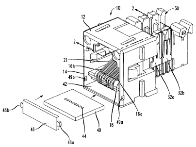
FIG. 1 is a perspective view of a communication
connector showing an electrical upgrade component about to
be positioned in the connector, according to a first
embodiment of the invention;
FIG. 2 is a view of the connector as seen in
cross-section along line 2-2 in FIG. 1; and
FIG. 3 is a side view in cross-section of a
communication connector and an electrical upgrade component
according to a second embodiment of the invention.
CA 02290088 2002-10-17
4
Detailed Description Of The Invention
FIG. 1 is a perspective view of a communication
connector 10 according to a first embodiment of the
invention. In the illustrated embodiment, connector 10 is a
telephone cable jack connector having an overall
construction similar to one disclosed in U.S. Patent No.
5,096,442 issued Mar. 17, 1992, but with certain
improvements allowing the connector 10 to be modified at the
user's option to enhance its electrical performance, as
explained below. Connector 10 has a housing 12 in the form
of a dielectric, i.e., non-electrically conductive material
(e. g., polycarbonate, ABS, and blends thereof) which
material meets all applicable standards with respect to
electrical insulation and flammability.
The connector housing 12 has a front opening 14 for
receiving a mating connector (not shown in FIG. 1). A
number of elongate electrically conductive connector
terminals in the form of, for example, eight elongated
spring jackwires 16a-16h are supported by a jackwire block
18 inside the housing 12. Upper, free ends of the jackwires
16a-16h are seated in corresponding vertical slots which are
formed in a partial wall 20 within the housing 12. The
slots act to guide and to keep each of the jackwires 16a-16h
separated from one another as they deflect downward when a
plug connector is inserted through the housing front opening
14. Wire terminals exposed on the plug connector may then
establish electrical contact with first end portions 21 of
the jackwires, inside the housing 14.
CA 02290088 1999-11-22
Connector 10 also has an associated terminal
housing 30 which may be formed of the same or similar
dielectric material as the connector housing 12. The
terminal housing 30 is fixed against a rear surface of the
5 connector housing as viewed in FIG. l, and substantially
encloses, for example, eight jackwire terminals 32a-32h.
See FIGS. 2 and 3. The jackwire terminals 32a-32h may be
in the form of known insulation displacement connector
(IDC) terminals that allow an insulated wire (not shown) to
make electrical contact with a given one of the jackwire
' terminals 32a-32h by sliding the wire down an exposed, open
slot (e.g., slot 33a in FIG. 2) in the given terminal. In
the illustrated embodiments, the jackwire terminals 32a-32h
are formed in connection with second end portions 33 of the
spring jackwires 16a-16h, and thus allow electrical
connections to be made between the jackwires and outside
circuits through wires that are inserted in the slots of
the jackwire terminals.
The jackwire block 18 may also be formed
integrally with the terminal housing 30 and, in the
illustrated embodiments, the jackwire block 18 protrudes
through an opening 34 in the rear surface of the connector
housing 12. Further details concerning the terminal
housing 30, the spring jackwires, jackwire terminals, and
the jackwire block may be found in the mentioned U.S.
Patent 5,096,442.
To upgrade the electrical performance
characteristics of the connector 10, an electrical upgrade
component 40 which may be in the form of a printed circuit
or wire board, can be incorporated in the connector 10 by
inserting the component 40 through the front opening 14 of
the connector housing 12. Component 40 may be, for
example, a single or multi-layer dielectric board having
CA 02290088 1999-11-22
6
wire traces printed on one or more layers, or any structure
that supports or contains parts capable of electrically
interacting with the jackwires 16a-16h, to affect the
performance of the connector 10. Such parts, alone or in
combination with other discrete devices carried by the
component 40, serve to reduce or cancel crosstalk that
would otherwise be produced across certain ones of the
jackwires 16a-16h when another connector is joined to the
connector 10. See the earlier mentioned '391 application.
In the disclosed embodiment, an upgrade component
space or passage 42 is formed in the connector housing 12,
in a region just below the jackwire block 18 as viewed in
the drawing. When the component 40 is positioned in the
passage 42, one or more contact pads 44 on an upper surface
of the component 40 establish electrical connections with
corresponding contact portions 46 formed in the jackwires
16a-16h. As shown in FIGS. 2 and 3, the contact portions
46 may be in the form of "bumps" in the jackwires which
protrude arcuately beneath the jackwire block 18, and
extend into the upgrade component passage 42 by an amount
sufficient to confront the upper surface of the component
40, when the component is placed in the passage 42. The
contact pads 44 are so located on the component 40 as to
make electrical contact with corresponding contact portions
46 on the jackwires, when the component is fully inserted
in the passage 42.
In the embodiment of FIGS. 1 and 2, the component
40 is blocked against further displacement toward the rear
of the connector housing 12 by an upstanding lip 50 at the
rear of the housing 12. The contact pads 44 on the
component 40 and the contact portions 46 of the jackwires
16a-16h, may be gold plated or otherwise treated to
maintain reliable electrical connections with one another
CA 02290088 1999-11-22
7
and to prevent corrosion during use. Importantly, even in
the absence of the component 40, the connector 10 will
nonetheless operate at a known level of performance.
An elastic, generally rectangular cover or door
48 has a pair of side ears 48a, 48b which are shown in FIG.
1. When the upgrade component 40 is fully inserted in the
passage 42, the cover 48 can be snapped in corresponding
slots 49a, 49b formed in side walls of the component
passage 42, near the front face of the connector housing
12. In addition to protecting the upgrade component 40 and
the jackwires 16a-16h from the outside environment, cover
48 prevents the upgrade component from moving away from a
position where it electrically contacts certain contact
portions 46 of the jackwires inside the connector housing
12.
The cover 48 may be marked for circuit
identification such as "Line 1,", "Data", "Ext. 40", or the
like, and may also be available in various colors for user
identification of the connector 10. If the component 40 is
not placed in the passage 42, the cover 48 may still be
snapped in position to shield the passage 42 and the
jackwire contact portions 46 from dirt and debris that
could otherwise enter the passage 42.
FIG. 2 is a side view of the connector 10 taken
in section along line 2-2 in FIG. 1. As shown, when the
upgrade component 40 is fully inserted in the passage 42,
contact pads 44 on the surface of the component make
electrical contact with corresponding contact portions 46
of the jackwires 16a-16h. Not all jackwires or pairs of
jackwires may require electrical compensation via the
component 40 to achieve various levels of performance. For
example, only the center four jackwires 16c-16f may require
CA 02290088 1999-11-22
8
additional compensation to meet the mentioned Category 5
performance requirements.
It can be seen in FIG. 2 that when a mating plug
is inserted in the connector front opening 14, the plug
will apply deflecting forces in the direction of arrow 54
on the free ends of the jackwires 16a-16h, above the
jackwire block 18. These forces are conducted to the
contact portions 46 of the jackwires in such a way as to
urge the contact portions further against the contact pads
44 on an inserted upgrade component 40. That is, the
jackwires tend to pivot about a front end 56 of the
jackwire block 18 in a clockwise direction as viewed in
FIG. 2, when the plug 52 is joined to the connector 10.
The front end 56 of the jackwire block may be formed with a
curvilinear cross-section as in FIG. 2, so as to prevent
the spring jackwires 16a-16h from bending permanently at
the front end of the block 18 when a plug is inserted in
the connector front opening 14.
FIG. 3 shows an arrangement wherein an upgrade
component 140 is installed from the rear of a connector
housing 112. Parts the same or similar to those shown in
FIGS. 1 and 2 have corresponding reference numerals
increased by 100 in FIG. 3.
In FIG. 3, the connector housing has a front lip
150 that covers one end of an upgrade component passage
142, at the front of connector housing 112. The housing
112 has a front opening 114 for receiving a mating
connector (not shown). A rear surface of the connector
housing 112 has an opening 134 for receiving a jackwire
block 118 of a terminal housing 130, with spring jackwires
116a-116h supported around the block 118.
CA 02290088 1999-11-22
9
The upgrade component 140 is positioned in the
passage 142 by inserting the component 140 through the
opening 134, until a leading end of the component abuts the
front lip 150 of the connector housing. The jackwire block
118 with the jackwires 116a-116h is then inserted through
the housing rear opening 134, until a base part 160 of the
terminal housing 130 abuts a rear body part 162 of the
connector housing 112. When so joined to the connector
housing 112, the terminal housing 130 covers the rear
opening 134 in the connector housing 112 including the
upgrade component passage 142. The terminal housing 130
also acts to maintain the upgrade component 140 at an
operative position in the passage 142 where contact pads
144 on the component establish electrical connections with
corresponding contact portions 146 of the jackwires 116a-
116h. As in the embodiment of FIGS. 1 and 2, the connector
is operative with a certain level of performance even if
the upgrade component 140 is withdrawn from the connector
housing 112.
For applications that require relatively low
performance, the connector 10 may be used without the
upgrade component 40 (or 140). This would allow a "least
costly" version of the connector 10.~ For higher levels of
performance, the component 40 with appropriate electrical
compensation may be added. For example, wire traces on or
within a component printed wire board could be configured
in a known manner to enhance performance by adding
capacitive crosstalk, thus allowing the connector 10 to
perform at higher data transmission rates.
Components 40 in the form of printed wire boards
having different trace configurations could be used to
achieve different levels of performance. The boards may be
comprised of multiple layers of wire traces alone or in
CA 02290088 1999-11-22
combination with discrete components, to facilitate the
performance enhancement. Any future improvements made
available by way of an upgrade component similar to the
component 40 may be incorporated in the connector 10,
5 without requiring any modification of remaining parts of
the connector, or of its assembly operations.
The connector 10 may also be upgraded in the
field by adding or replacing an existing component 40 with
an improved one. This is a very useful feature as data
10 transmission rates continue to increase resulting in higher
performance requirements for communication connectors.
While the foregoing description represents
preferred embodiments of the invention, it will be obvious
to those skilled in the art that various changes and
modifications may be made, without departing from the true
spirit and scope of the invention.